
A 12-Bit 50 MS/s Split-CDAC-Based SAR ADC Integrating Input Programmable Gain Amplifier and Reference Voltage Buffer

 ,
,
Abstract
:1. Introduction
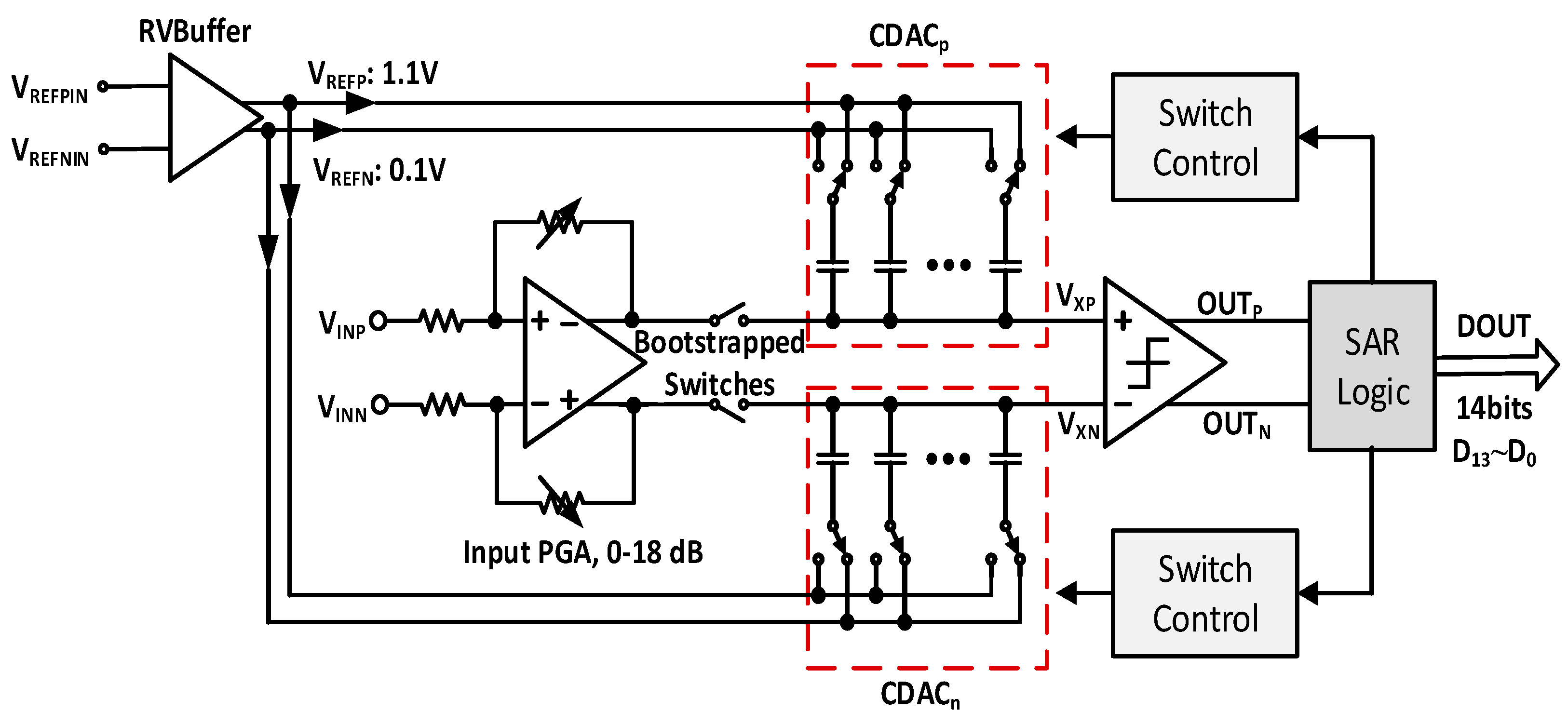
2. Overall Architecture
3. Circuit Implementation
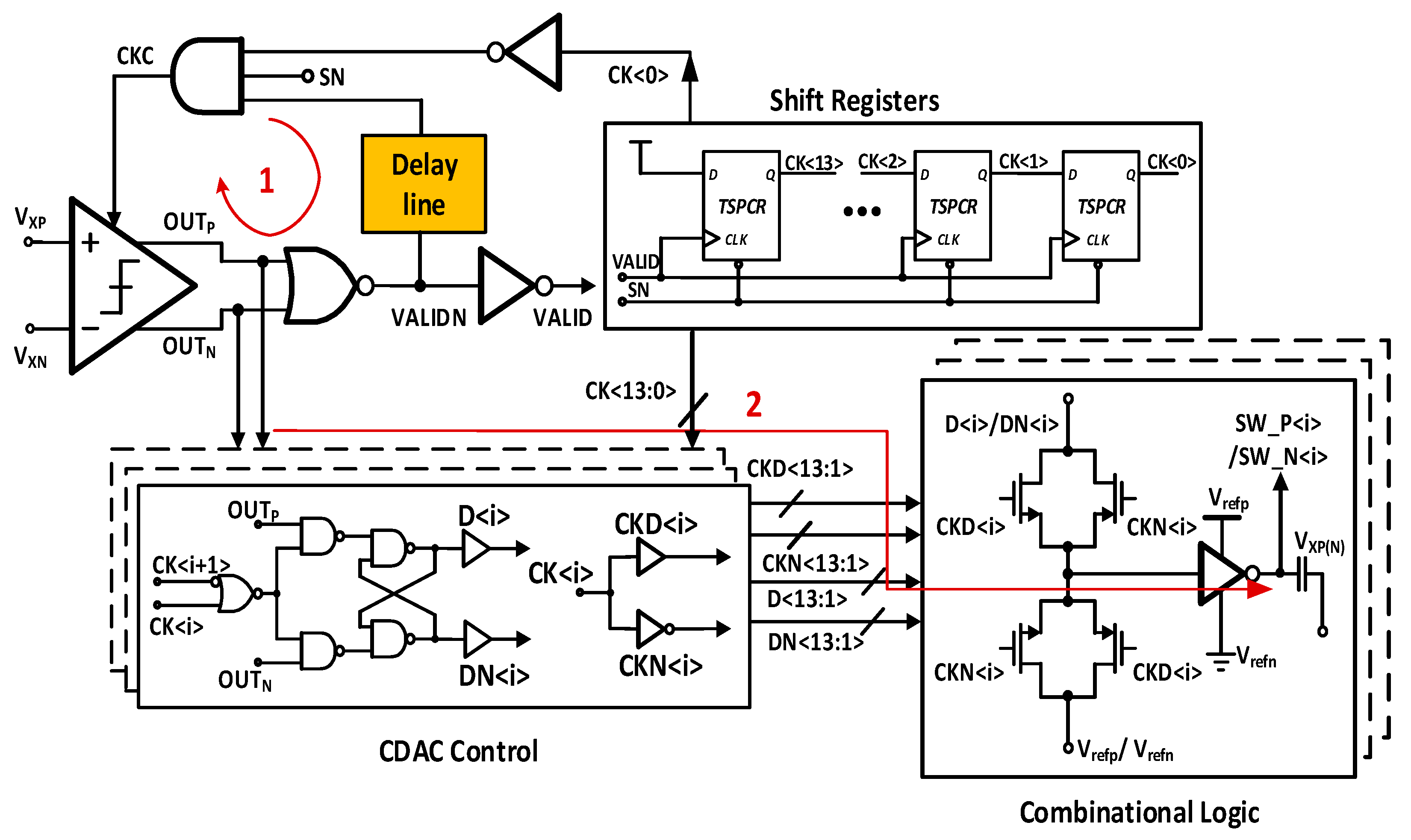
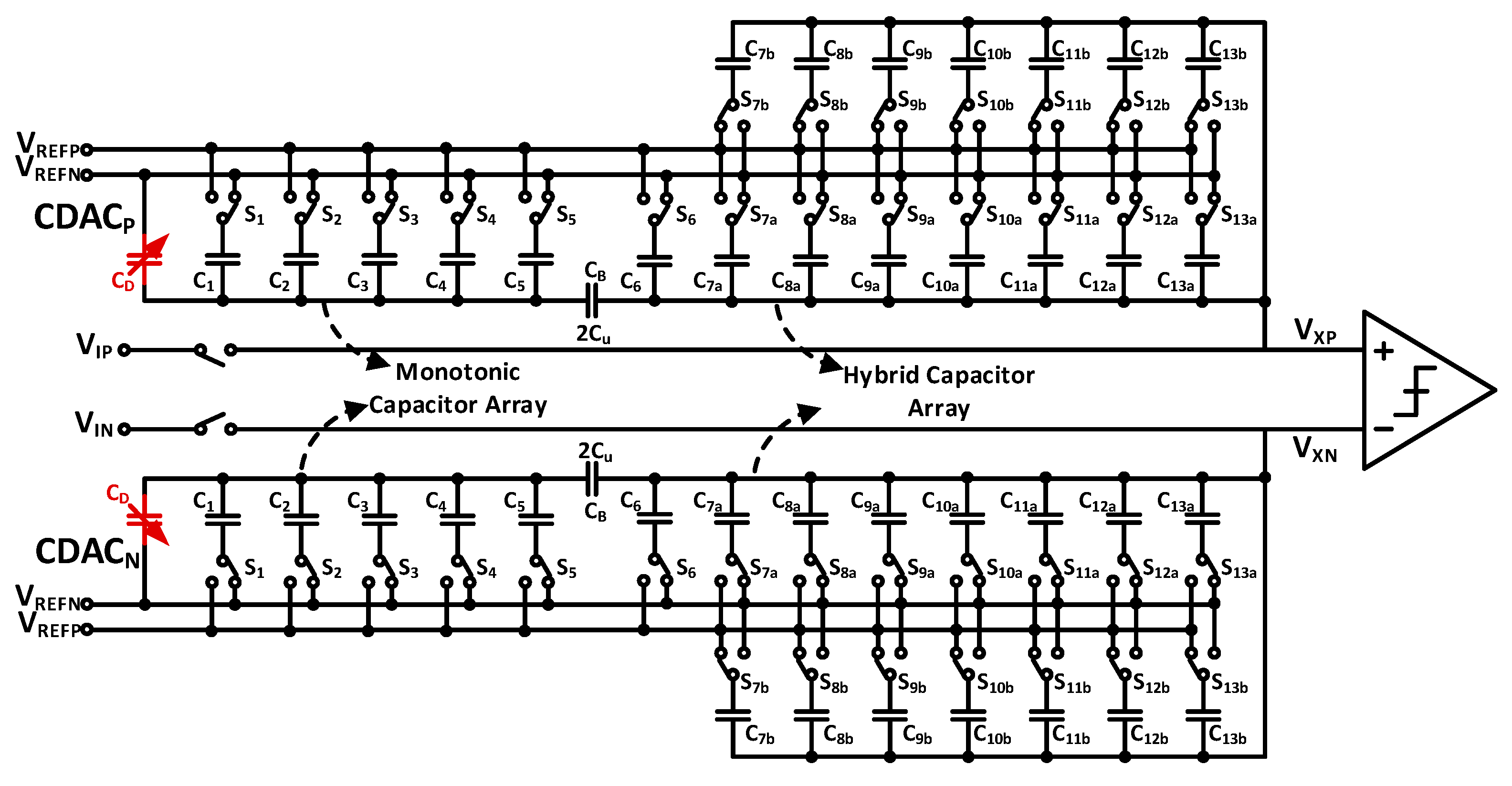
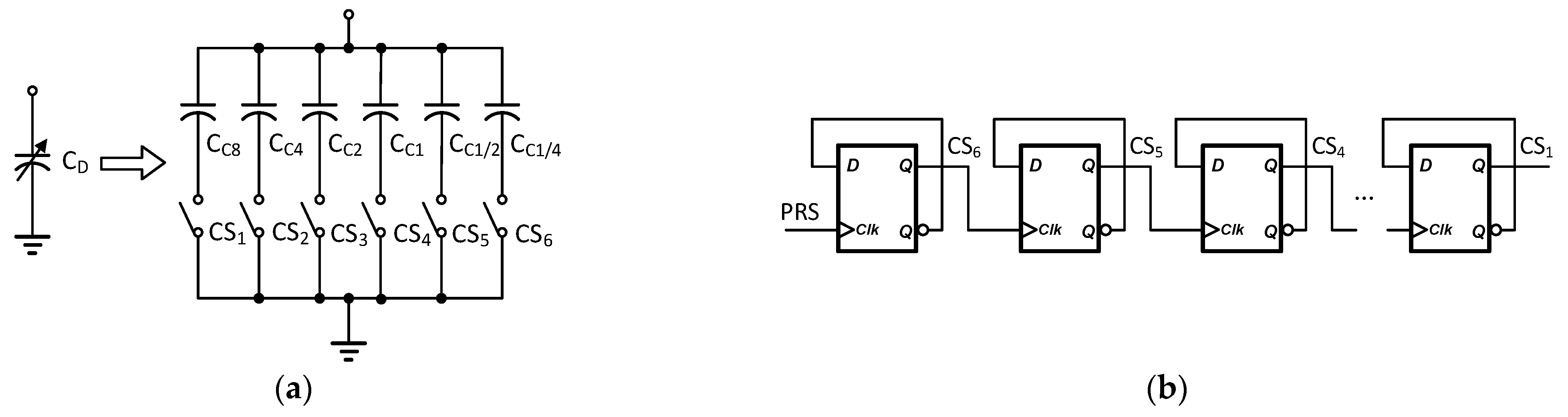
3.1. Split CDAC
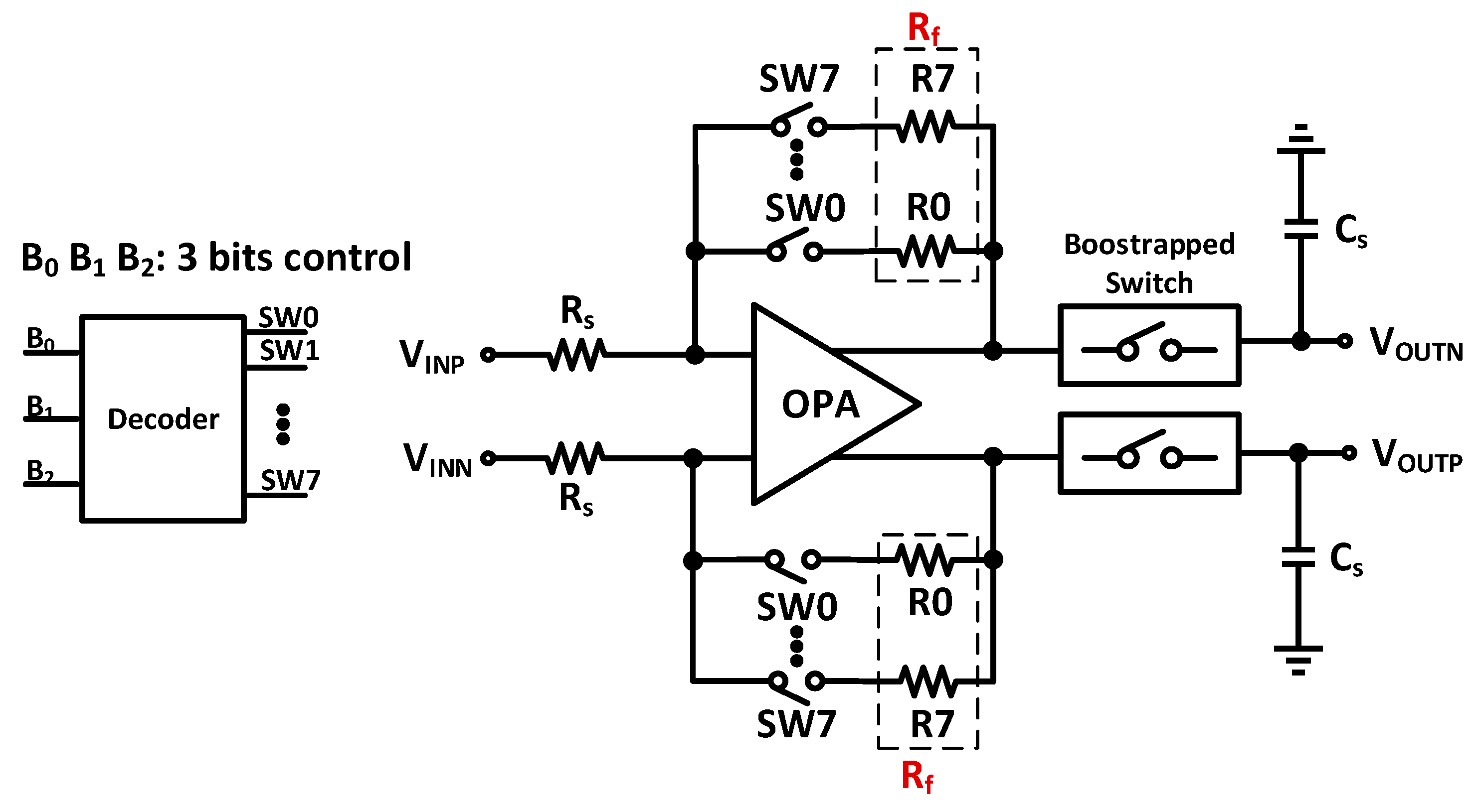
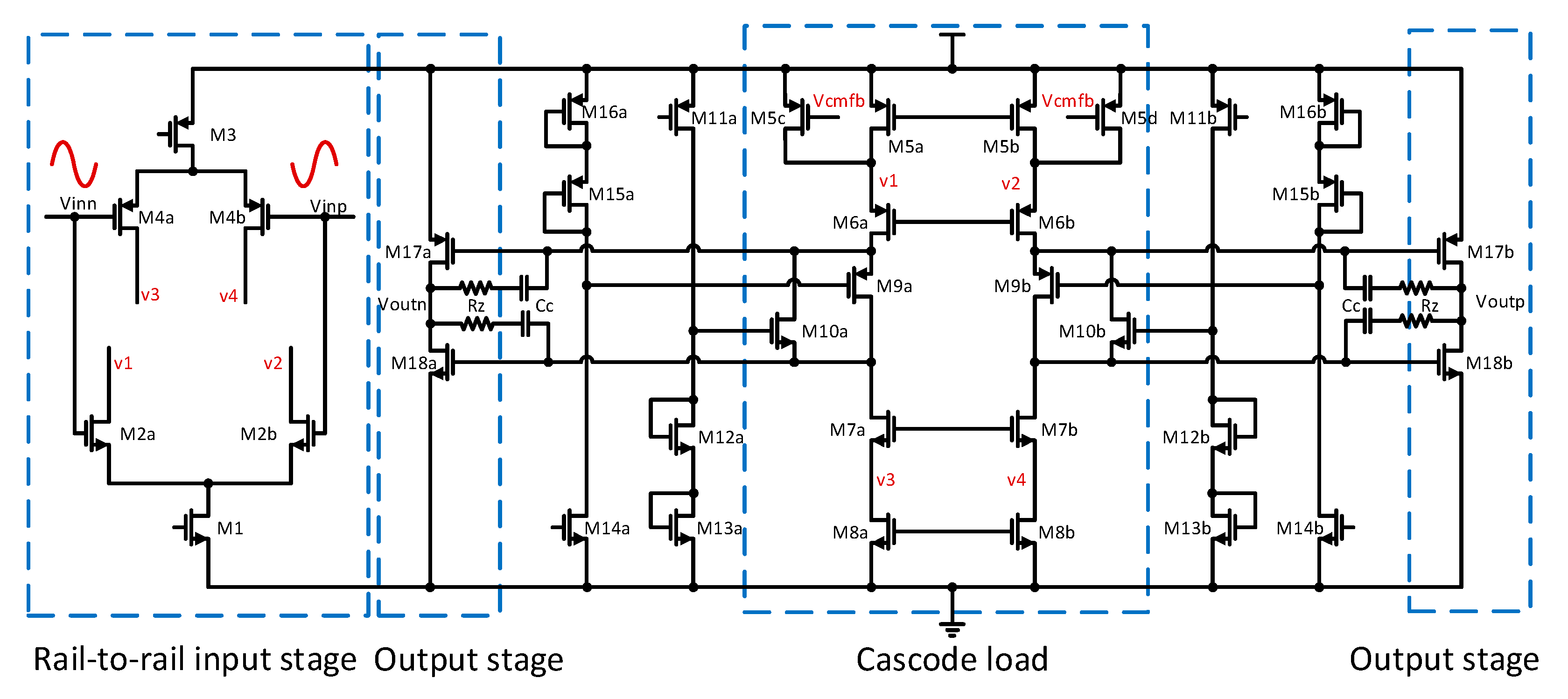
3.2. Input PGA
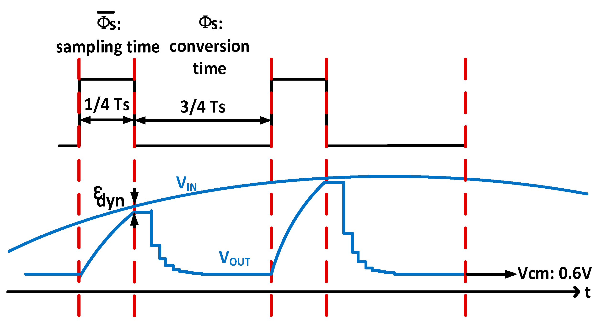
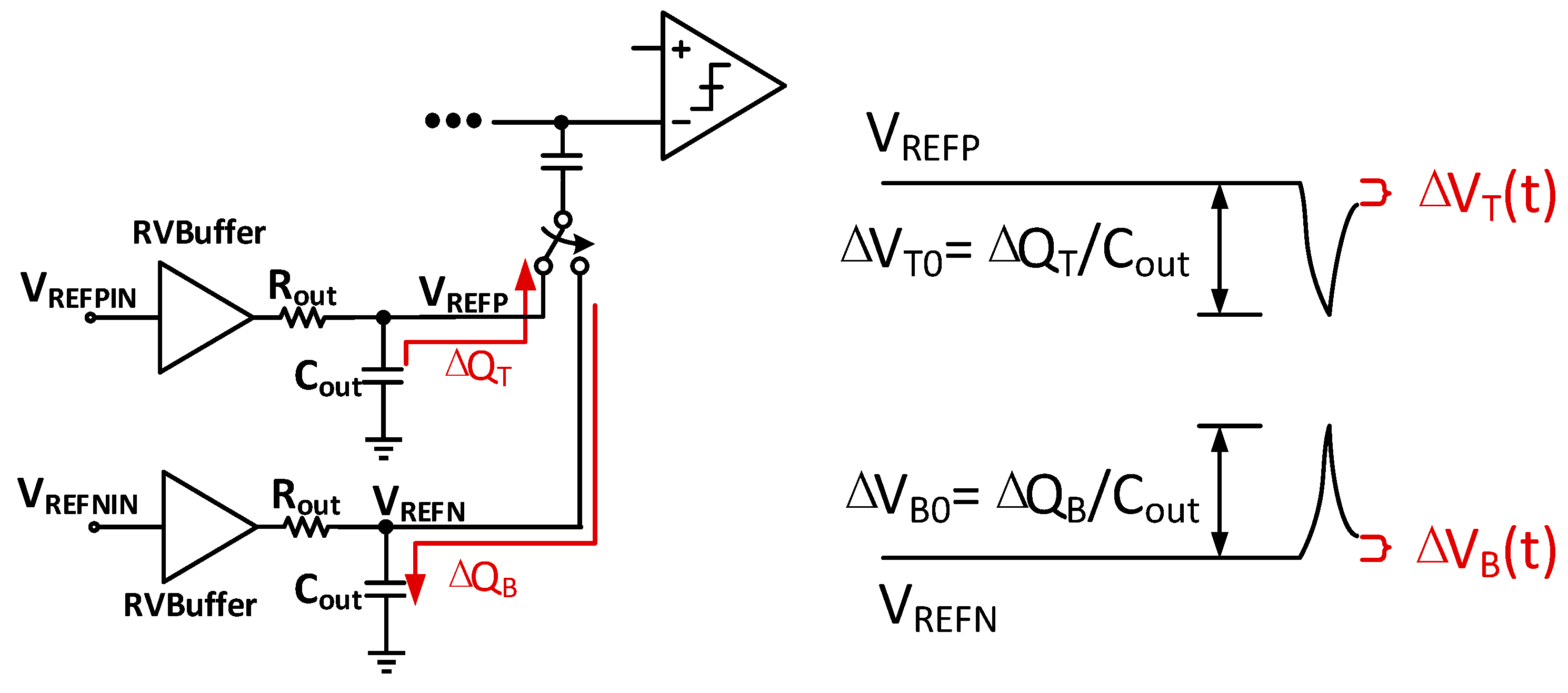
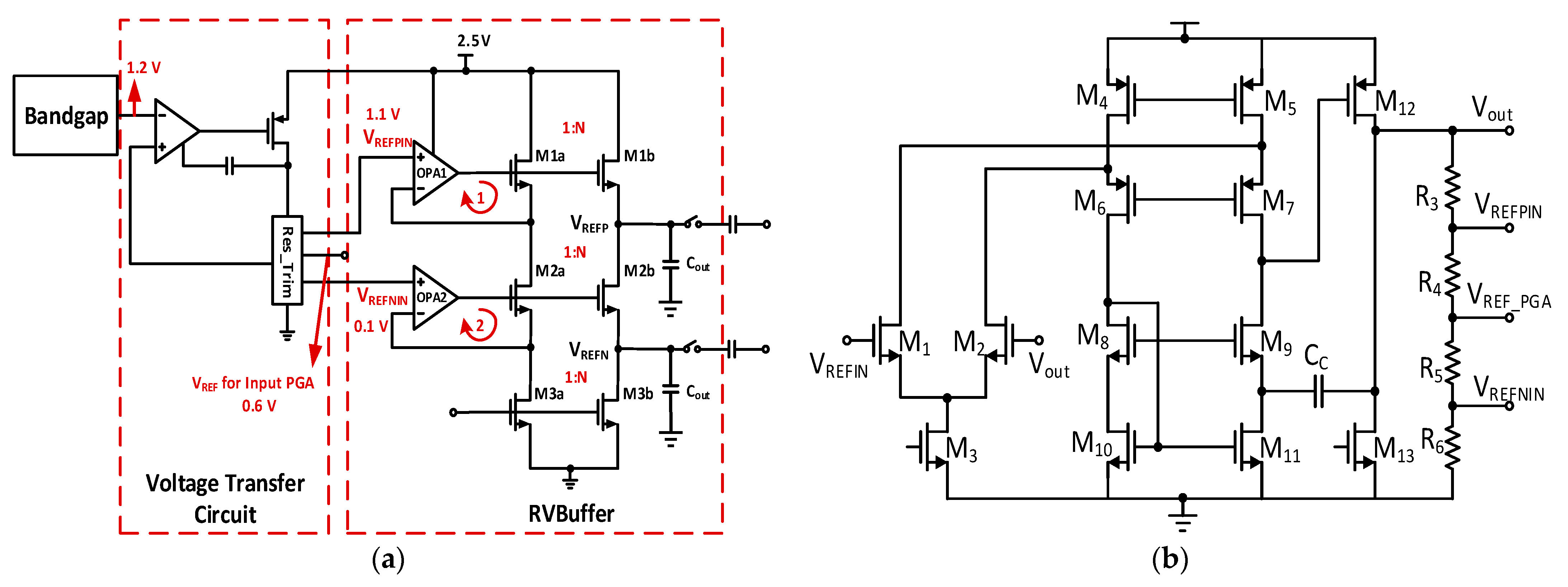
3.3. RV-Buffer
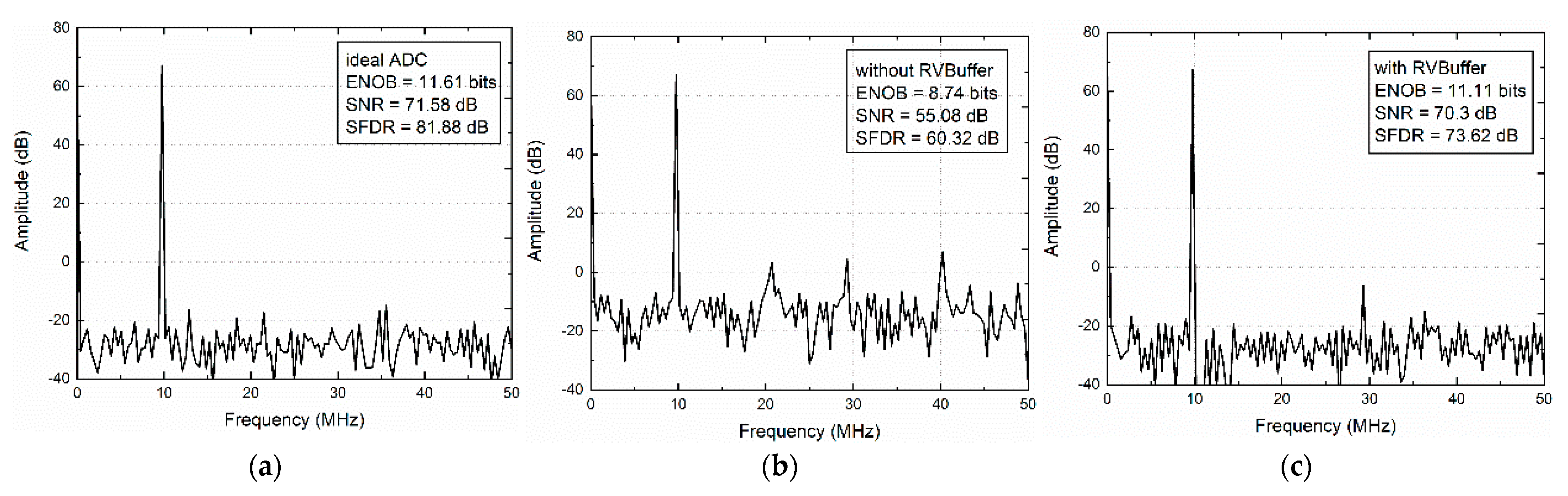
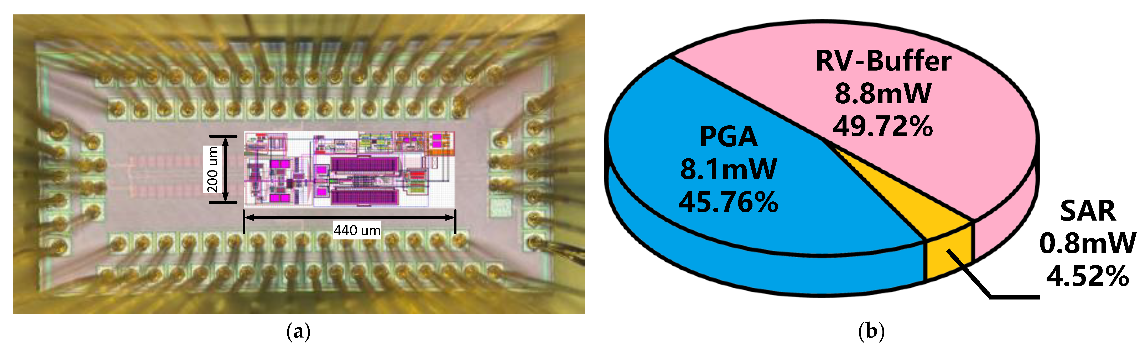
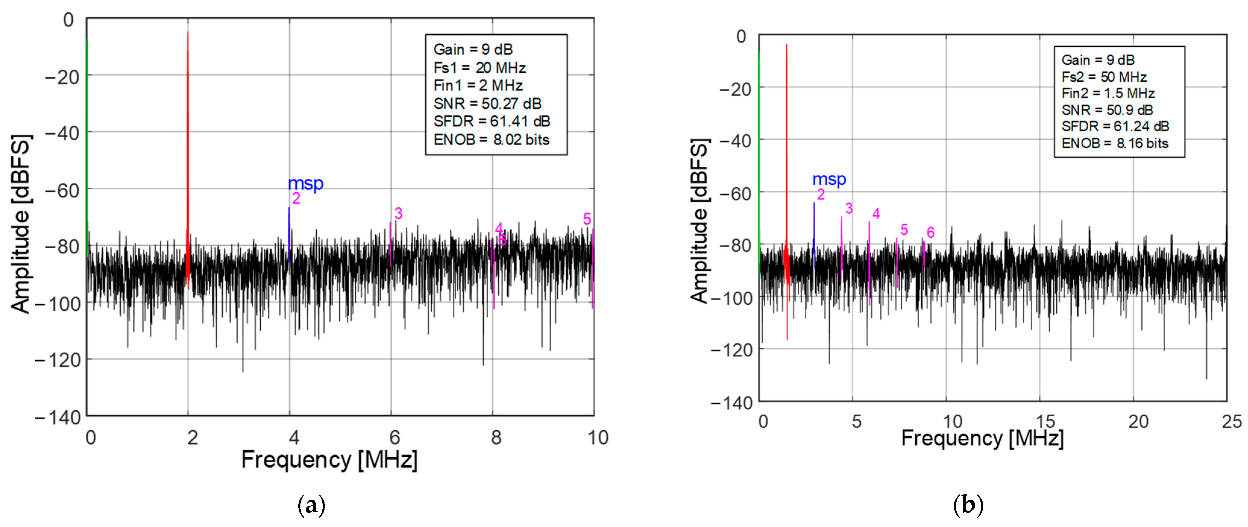
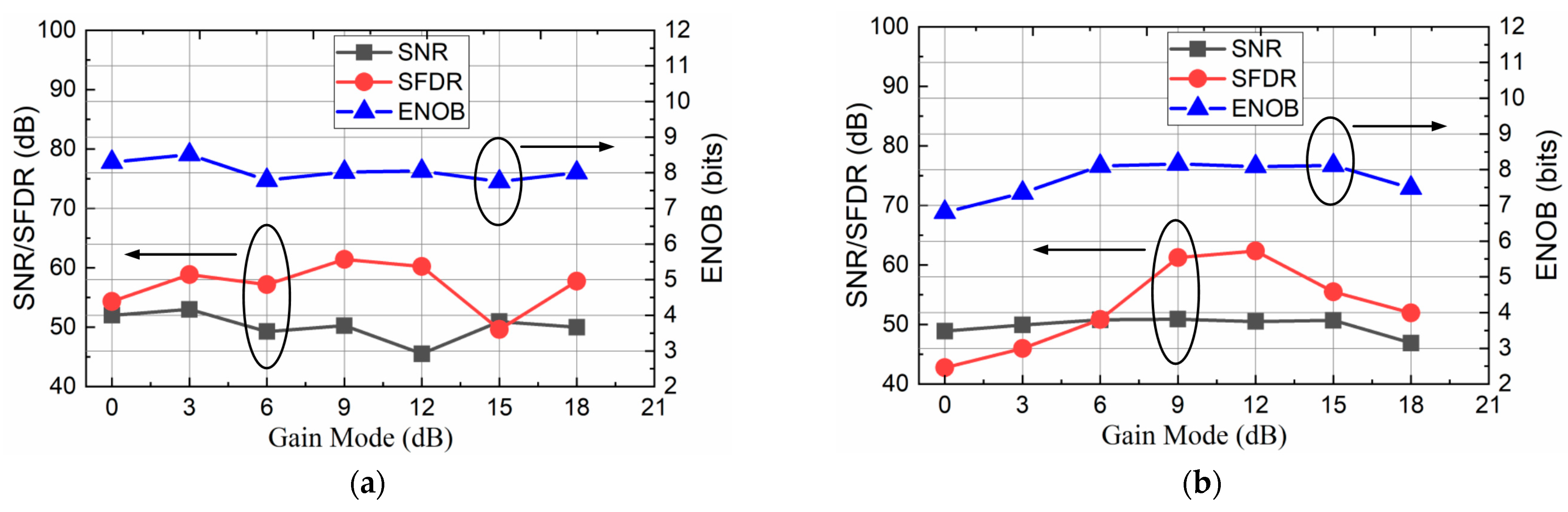
4. Measurement Results
5. Conclusions
Author Contributions
Funding
Conflicts of Interest
References
- Chan, C.; Zhu, Y.; Cheng, L.; Zhang, W.; Ho, l.; Wei, L.; Seng-Pan, U.; Martins, R. 60-dB SNDR 100-MS/s SAR ADCs With Threshold Reconfigurable Reference Error Calibration. IEEE J. Solid-State Circuits 2017, 52, 2576–2588. [Google Scholar] [CrossRef]
- Liu, C.; Kuo, C.; Lin, Y. A 10 bit 320 MS/s Low-Cost SAR ADC for IEEE 802.11ac Applications in 20 nm CMOS. IEEE J. Solid-State Circuits 2015, 50, 2645–2654. [Google Scholar] [CrossRef]
- Inerfield, M.; Kamath, A.; Su, F.; Hu, J.; Yu, X.; Fong, V.; Alnaggar, O.; Lin, F.; Kwan, T. An 11.5-ENOB 100-MS/s 8 mW dual-reference SAR ADC in 28 nm CMOS. In Proceedings of the 2014 IEEE Symposium on VLSI Circuits Digest of Technical Ppaers, Honolulu, HI, USA, 10–13 June 2014. [Google Scholar]
- Bindra, H.S.; Annema, A.; Wienk, G.; Nauta, B.; Louwsma, S.M. A 4MS/s 10b SAR ADC with integrated Class-A buffers in 65nm CMOS with near rail-to-rail input using a single 1.2 V supply. In Proceedings of the 2019 IEEE Custom Integrated Circuits Conference, Austin, TX, USA, 14–17 April 2019. [Google Scholar]
- Tseng, W.; Lee, W.; Huang, C.; Chiu, P. A 12-bit 104 MS/s SAR ADC in 28 nm CMOS for Digitally-Assisted Wireless Transmitters. IEEE J. Solid-State Circuits 2016, 51, 2222–2231. [Google Scholar] [CrossRef]
- Wang, J.; Liu, S.; Shen, Y.; Zhu, Z. Low-Power Single-Ended SAR ADC Using Symmetrical DAC Switching for Image Sensors With Passive CDS and PGA Technique. IEEE Trans. Circuits Syst. I Reg. Pap. 2018, 65, 2378–2388. [Google Scholar] [CrossRef]
- Choi, M.; Ahn, G.; Lee, S. 12b 50MS/s 0.18 μm CMOS ADC with highly linear input variable gain amplifier. Electron. Lett. 2010, 46, 1254–1256. [Google Scholar] [CrossRef]
- El-Nozahi, M.; Amer, A.; Torres, J.; Entesari, K.; Sanchez-Sinencio, E. High PSR Low Drop-Out Regulator With Feed-Forward Ripple Cancellation Technique. IEEE J. Solid-State Circuits 2010, 45, 565–577. [Google Scholar] [CrossRef]
- Huang, G.Y.; Chang, S.; Liu, C.; Lin, Y. 10-bit 30-MS/s SAR ADC using a switchback switching method. IEEE Trans. Very Large Scale Integr. Syst. 2012, 21, 584–588. [Google Scholar] [CrossRef]
- Li, M.; Yao, Y.; Hu, B.; Wei, J.; Chen, Y.; Ma, S.; Ye, F.; Ren, J. A 6.94-fJ/Conversion-Step 12-bit 100-MS/s Asynchronous SAR ADC Exploiting Split-CDAC in 65 nm CMOS. IEEE Access 2021, 9, 77545–77554. [Google Scholar] [CrossRef]
- Wang, Z.; Chen, Y.; Qian, H. A 1.5GS/s 6bit 2bit/step Asynchronous Time Interleaved SAR ADC in 65nm CMOS. China Semicond. Technol. Int. Conf. (CSTIC) 2012, 44, 121. [Google Scholar] [CrossRef]
- Sunny, S.; Chen, Y.; Boon, C. A 4.06-mW 10-bit 150-MS/s SAR ADC with 1.5-bit/cycle Operation for Medical Imaging Applications. IEEE Sens. J. 2018, 18, 4553–4560. [Google Scholar] [CrossRef]
- Um, J.; Kim, Y.; Song, E.; Sim, J.; Park, H. A digital-domain calibration of split-capacitor dac for a differential sar adc without additional analog circuits. IEEE Trans. Circuits Syst. I Reg. Pap. 2013, 60, 2845–2856. [Google Scholar] [CrossRef]
- Chen, Y.; Zhu, X.; Tamura, H.; Kibune, M.; Tomita, Y.; Hamada, T.; Yoshioka, M.; Ishikawa, K.; Takayama, T.; Ogawa, J.; et al. Split capacitor DAC mismatch calibration in successive approximation ADC. In Proceedings of the 2009 IEEE Custom Integrated Circuits Conference, San Jose, CA, USA, 13–16 September 2009. [Google Scholar]
- Ginsburg, B.P.; Chandrakasan, A.P. 500-MS/s 5-bit ADC in 65-nm CMOS with split capacitor array DAC. IEEE J. Solid-State Circuits 2007, 42, 739–747. [Google Scholar] [CrossRef]
- Liu, C.C.; Chang, S.J.; Huang, G.Y.; Lin, Y.Z. A 10-bit 50 MS/s SAR ADC with a monotonic capacitor switching procedure. IEEE J. Solid-State Circuits 2010, 45, 731–740. [Google Scholar] [CrossRef]
- Ballo, A.; Grasso, A.D.; Pennisi, S. Active load with cross-coupled bulk for high-gain high-CMRR nanometer CMOS differential stages. Int. J. Circ. Theor. Appl. 2019, 47, 1700–1704. [Google Scholar] [CrossRef]
- Hsu, Y.; Liu, Z.; Hella, M.M. A-68 dB THD, 0.6 mm2 Active Area Biosignal Acquisition System With a 40–320 Hz Duty-Cycle Controlled Filter. IEEE Trans. Circuits Syst. I Reg. Pap. 2020, 67, 48–59. [Google Scholar] [CrossRef]
- Hogervorst, R.; Tero, J.P.; Eschauzier, R.G.H.; Huijsing, J.H. A compact power-efficient 3 V CMOS rail-to-rail input/output operational amplifier for VLSI cell libraries. IEEE J. Solid-State Circuits 1994, 29, 1505–1513. [Google Scholar] [CrossRef] [Green Version]
- Ballo, A.; Grasso, A.D.; Giustolisi, G.; Palumbo, G. Optimized Charge Pump With Clock Booster for Reduced Rise Time or Silicon Area. IEEE Trans. Circuits Syst. II Express Briefs 2019, 66, 1977–1981. [Google Scholar] [CrossRef]
- Ballo, A.; Grasso, A.D.; Palumbo, G.; Tanzawa, T. Linear distribution of capacitance in Dickson charge pumps to reduce rise time. Int. J. Circ. Theor. Appl. 2020, 48, 555–566. [Google Scholar] [CrossRef]
- Lu, C.C.; Huang, D.K. 1.2 V 10-bits 40 MS/s CMOS SAR ADC for low-power applications. IET Circuits Devices Syst. 2019, 13, 857–862. [Google Scholar] [CrossRef]
- Park, J.S.; Kim, D.H.; An, T.J.; Kim, M.K.; Ahn, G.C.; Lee, S.H. 12 b 50 MS/s 0.18 μm CMOS SAR ADC based on highly linear C-R hybrid DAC. Electron. Lett. 2020, 56, 119–121. [Google Scholar] [CrossRef]

| Supply Voltage | 1.2 V | Output Swing | 1.8 Vpp.diff |
| Common mode Output Voltage | 0.6 V | DC Current | 6.78 mA |
| DC Gain | 77 dB | GBW | 1.95 GHz |
| Phase Margin | 50° | IRN | 1.52 nV/√Hz |
| This Work | [6] | [7] | [22] | [23] | |
|---|---|---|---|---|---|
| Architecture | PGA + ADC + RV-Buffer | PGA + ADC | PGA + ADC | ADC | ADC |
| Technology | 65 nm | 65 nm | 0.18 μm | 0.18 μm | 0.18 μm |
| Supply Voltage (V) | 1.2/2.5 * | 1.2 | 1.8 | 1.2 | 1.2 |
| PowerADC (mW) | 0.8 | 0.26 | 22.2 | 0.736 | 4.734 |
| PowerPGA (mW) | 8.1 | 0.16 | 5.9 | / | / |
| Gain Range (dB) | 0~18 | −6, 0, 6 | −3~0 | / | / |
| Resolution (bits) | 12 | 10 | 12 | 10 | 12 |
| Sampling Frequency (MS/s) | 50 | 40 | 50 | 40 | 50 |
| Input Range for ADC (Vpp) | 1.8 | 0.88 | 1.5 | 1 | 1.4 |
| ENOBpeak | 8.16 | 9 | 10 | 9.13 | 10.4 |
| SNRpeak | 50.9 | / | / | 56.7 | 64.3 |
| SFDRpeak | 62.35 | 72 | 73.1 | 65.8 | 74.7 |
| FoMADC (fJ/conv.-step) ** | 55.9 | 21.7 *** | 433.6 | 32.84 *** | 70.6 *** |
Publisher’s Note: MDPI stays neutral with regard to jurisdictional claims in published maps and institutional affiliations. |
© 2022 by the authors. Licensee MDPI, Basel, Switzerland. This article is an open access article distributed under the terms and conditions of the Creative Commons Attribution (CC BY) license (https://creativecommons.org/licenses/by/4.0/).
Share and Cite
Xu, Z.; Hu, B.; Wu, T.; Yao, Y.; Chen, Y.; Ren, J.; Ma, S. A 12-Bit 50 MS/s Split-CDAC-Based SAR ADC Integrating Input Programmable Gain Amplifier and Reference Voltage Buffer. Electronics 2022, 11, 1841. https://doi.org/10.3390/electronics11121841
Xu Z, Hu B, Wu T, Yao Y, Chen Y, Ren J, Ma S. A 12-Bit 50 MS/s Split-CDAC-Based SAR ADC Integrating Input Programmable Gain Amplifier and Reference Voltage Buffer. Electronics. 2022; 11(12):1841. https://doi.org/10.3390/electronics11121841
Chicago/Turabian StyleXu, Zhuofan, Biao Hu, Tianxiang Wu, Yuting Yao, Yong Chen, Junyan Ren, and Shunli Ma. 2022. "A 12-Bit 50 MS/s Split-CDAC-Based SAR ADC Integrating Input Programmable Gain Amplifier and Reference Voltage Buffer" Electronics 11, no. 12: 1841. https://doi.org/10.3390/electronics11121841
APA StyleXu, Z., Hu, B., Wu, T., Yao, Y., Chen, Y., Ren, J., & Ma, S. (2022). A 12-Bit 50 MS/s Split-CDAC-Based SAR ADC Integrating Input Programmable Gain Amplifier and Reference Voltage Buffer. Electronics, 11(12), 1841. https://doi.org/10.3390/electronics11121841