Article

An 8-Gbps, Low-Jitter, Four-Channel Transmitter with a Fractional-Spaced Feed-Forward Equalizer

1
Institute of Microelectronics, Chinese Academy of Sciences, Beijing 100029, China
2
School of Integrated Circuits, University of Chinese Academy of Sciences, Beijing 100049, China
*
Author to whom correspondence should be addressed.
Electronics 2022, 11(11), 1768; https://doi.org/10.3390/electronics11111768
Submission received: 10 May 2022 / Revised: 28 May 2022 / Accepted: 31 May 2022 / Published: 2 June 2022
(This article belongs to the Section Microelectronics)

Abstract

:
An 8 gigabits per second (Gbps), low-jitter, four-channel transmitter with fractional-spaced feed-forward equalizer (FFE) is designed to meet the demand for broad transmission bandwidth in serial data communications. A novel frequency divider chain (FDC) architecture is developed, to satisfy the time requirements for high-speed data serialization. Moreover, a reconfigurable output driver circuit is employed to ensure compatibility with different protocols. In addition, a three-tap fractional-spaced FFE, which can enhance signal bandwidth significantly, is proposed, to compensate for channel loss. The transmitter was simulated and validated based on the Semiconductor Manufacturing International Corporation (SMIC) 55-nm process. The post-layout simulation results show the following: The tuning range of the phase-locked loop (PLL) can cover 1.6 to 4.6 GHz. At an output frequency of 4 GHz, the root-mean-square jitter (RJ) of the PLL after integration from phase noise was 1.93 ps. With an 8 Gbps output data rate, using the pseudo-random binary sequence (PRBS)-31 as a data source to simulate the whole transmitter, the power consumption values of the PLL and drive circuit were 27.0 and 29.2 mW, respectively, and the eye width and the valid eye height of output data were 0.76 unit interval (UI) and 0.68.

1. Introduction

High-speed serializer/de-serializer (SerDes) technology is extensively employed to improve the data transmission performance of wireline transmission systems [1]. Due to the continuous development of data-intensive services, such as the Internet of Things, cloud computing, and cloud storage, telecommunication infrastructure is required to be upgraded; therefore, the requirements for the data transmission rate of SerDes should be increased [2,3,4,5]. Therefore, the transmitter of SerDes must provide a high-speed data transfer rate and maintain the signal integrity, which is the main problem faced in the design.
A SerDes transmitter generally consists of two parts: a phase-locked loop (PLL), and a driver. The function of the PLL is to provide stable and high-accuracy clock signals [6,7,8]. Meanwhile, correct output data and sufficient signal swing are required for the driver [9,10]. From an application perspective, the driver needs to conform to different protocols. Moreover, because the integrity of high-speed signals is often affected by the channel loss of the transmission line, a feed-forward equalizer (FFE) is usually used in the driver, to compensate for channel loss [11,12,13]. In general, a baud-spaced FFE is usually used. However, the peak frequency of the baud-spaced FFE’s frequency response is the Nyquist frequency of the output data rate. Compared with the baud-spaced FFE, a fractional-spaced FFE can improve the peak frequency significantly; therefore, increasing the signal bandwidth after equalization. As a result, a fractional-spaced FFE can reduce signal aliasing effectively, and improve the integrity and performance of the equalized signal [14,15].
Against the above research background, in this article, we present a low-cost, low-power-consumption, low-jitter, four-channel SerDes transmitter that can transmit data at 8 gigabits per second (Gbps) and is compatible with multiple transmission protocols. The transmitter contains a type-II fourth-order PLL, which can provide a differential clock with high speed and low jitter. The multiplexers (MUXs) in the driver serialize 32-bit data. Moreover, a novel frequency divider chain (FDC) architecture is designed to satisfy the time requirements for high-speed serialization, with applicability for higher-speed transmitter architectures. Furthermore, a reconfigurable output driver that conforms to multiple protocols is developed. Finally, a three-tap fractional-spaced FFE is used to compensate for channel loss, which can enhance the signal bandwidth significantly.
This paper is organized as follows: Section 1 presents the introduction. Section 2 introduces the top architecture of the presented transmitter. Section 3 and Section 4 provide the circuit design implementation and details of the PLL and driver, respectively. The simulation results and discussions are given in Section 5. Finally, the conclusions are summarized in Section 6.

2. Top Architecture

Figure 1 shows a block diagram of the designed transmitter system.
A fourth-order PLL is adopted in the transmitter, which can enhance the ability to suppress the noise of vcon at high frequency, with a small price of chip area, and will not have a prominent influence on the PLL’s phase margin (vcon is the input voltage of the voltage-controlled oscillator (VCO)). Low-dropout regulators (LDOs) are used to supply power and reduce clock jitter. To fully satisfy the time requirements for the flip-flops (FFs) in the MUXs during high-speed applications, a novel clock FDC architecture is developed to divide the frequency of the clock signal output by the PLL. The frequency-divided clocks serve as a reference clock signal for a 32-to-1 MUX, while another 1/16-frequency-divided clock is input as a reference clock into a digital module. An encoder is used to generate 32-bit parallel data or pseudo-random binary sequence (PRBS) signals that are subsequently input into the transmitter for serialization. First, the 32-to-2 MUX transforms the parallel data to an odd data stream DODD and an even data stream DEVEN, and subsequently inputs them into a latch array and delay block, to generate a main cursor, a fractional cursor that is fractional unit interval (UI) behind the main cursor, and a postcursor that is one UI behind the main cursor. The proportion of the main-cursor, fractional cursor, and post cursor can be programmed to change the output swing of the transmitter, and to modify the range of de-emphasis, to compensate for the attenuation introduced by the different channels.

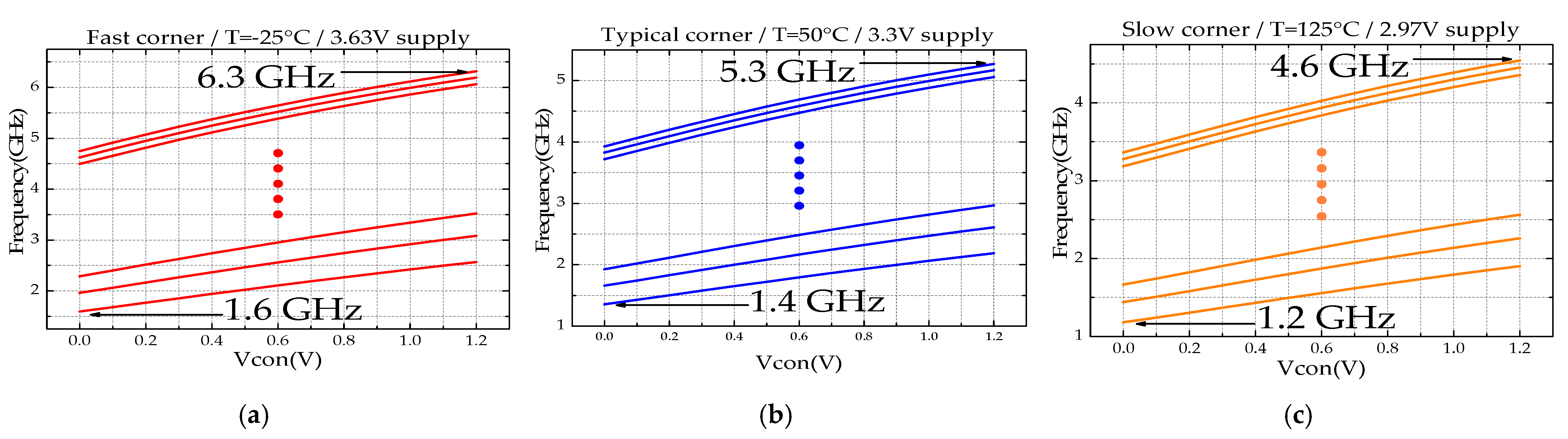
3. PLL Circuit Implementation

Figure 2 shows a block diagram of the designed PLL. The PLL consists of a predivider (PD), a phase frequency detector (PFD), a charge pump (CP), a third-order loop-filter (LPF), a ring VCO, a loop divider, and an output divider (OD).
An adjustable reset delay module is added to the PFD to eliminate the dead-zone effects with different sets of process–voltage–temperature (PVT) conditions. The CP uses two rail-to-rail operational amplifiers to reduce the drain-voltage fluctuations in the metal-oxide-semiconductor field-effect transistor (MOSFET) in the current supply, with the goal of mitigating the mismatch between the charge and discharge currents introduced by channel-length modulation [16]. Moreover, a ring VCO architecture is adopted to reduce the chip area and cost, while providing a broadband tuning range [17]. The PD and OD divide the frequency of the reference and output clocks, respectively, to expand the output frequency band of the PLL [18]. A two-stage LDO regulator chain is used to supply power to the components of the PLL. An LDO regulator with an output voltage of 1.8 V is used to supply power to the VCO alone. The CP, PFD, divider (DIV), and OD are high-frequency modules that operate at different frequencies. Therefore, to reduce the clock jitter caused by power-supply fluctuations, three LDO regulators with an output voltage of 1.2 V are used to supply power to these components [19].

4. Driver Circuit Implementation
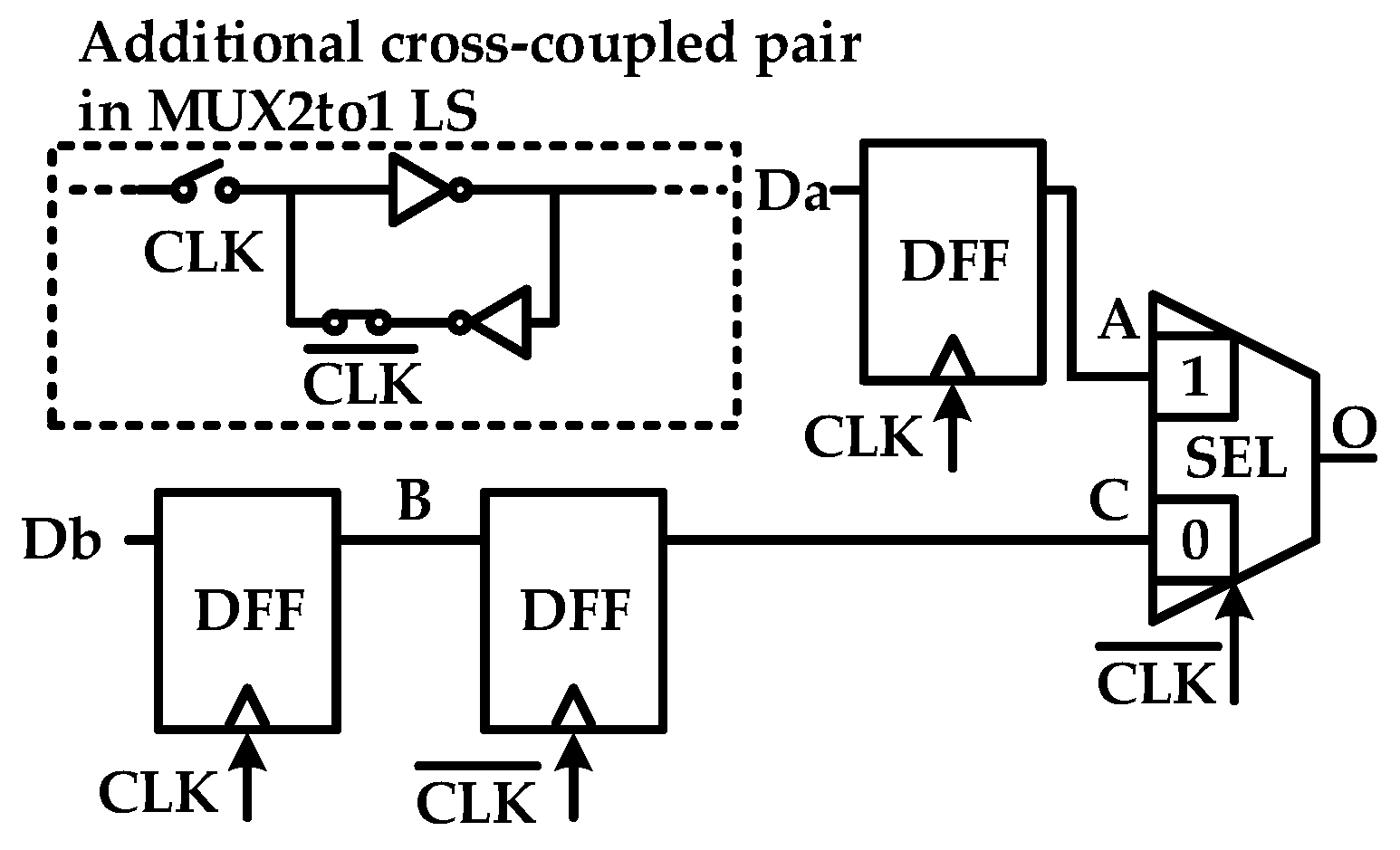
4.1. MUXs

MUXs in transmitters are responsible for transforming parallel data to high-speed serial data. The designed 32-to-1 MUX features a tree-shaped half-rate architecture, to reduce the timing constraints of the high-speed path [20], as shown in Figure 3.
For a half-rate architecture, the clock duty cycle (CDC) affects the output-signal jitter and, thus, needs to be corrected using a duty cycle corrector. The input of the high-speed clock output by the PLL into the clock frequency divider module generates 0-, 1/2-, 1/4-, 1/8-, and 1/16-frequency-divided differential clocks. These five pairs of clock s are successively used as the sampling clocks for different layers of the tree-shaped architecture, to serialize the parallel data level-by-level with the 2-to-1 MUX in Figure 4 as a basic unit.
As seen in Figure 4, the 2-to-1 MUX is composed of three D FFs (DFFs) and one selector. One data stream, Da, is sampled to point A at the rising edge of the CLK. Another data stream, Db, is sampled to point B at the rising edge of the CLK and subsequently sampled by a DFF to point C at the rising edge of the CLK ¯ . Therefore, point C is half a clock cycle behind point A. Finally, the selector outputs point C (Db) during a positive half cycle of CLK and point A (Da) during a negative half cycle of CLK, to double the data rate. An additional cross-coupled pair are included to prevent charge leakage in the low-speed MUX. The 32-to-2 MUX transforms the parallel data to DODD and DEVEN, which are subsequently passed through the latch array and the delay block to output the main cursor, fractional cursor, and post cursor. These cursors are ultimately input into the driver, to compensate the channel loss.

4.2. Clock FDC Architecture

In high-speed mode, the 2-to-1 MUX needs to fully meet the setup and hold time (TST and THD, respectively) requirements of the DFFs, to prevent errors [21]. A clock FDC architecture is developed in this study, as shown in Figure 5a. Figure 5b shows the corresponding timing diagram.
First, the PLL outputs a half-rate clock (CLKO). The CLKO is then buffered by a two-stage phase-inverter chain, to produce CLK1, then by a one-stage divide-by-two divider and a four-stage phase-inverter chain, to produce CLK2. The signal at the midpoint of the four-stage phase-inverter chain is input into the subsequent one-stage divide-by-two divider. The above process is then repeated. Ultimately, five clocks, CLK1, CLK2, CLK4, CLK8, and CLK16, are obtained. Let TCTD and TINV be the time delay of a one-stage divide-by-two divider and the time delay of a one-stage phase inverter, respectively. Then, the time delay of each CLK relative to the preceding CLK is calculated as follows:
T D E L A Y = T C T D + 4 T I N V 2 T I N V = T C T D + 2 T I N V .
For the 2-to-1 MUX in Figure 4, the time delay between the data at point O and the data at point A or C is equivalent to the time delay of the selector, TSEL. In addition, the initial data are generated by the digital module, with CLK16 as a reference clock, and have a width equivalent to the CLK16 cycle. The 2-to-1 MUX selects one out of the two data streams. This process requires CLK(2N) to be first used for selection. After TSEL, the selected data stream is sent to the subsequent 2-to-1 MUX for sampling. The width of the sampled data stream is half the CLK(2N) cycle. Here, the sampling of data stream D0 is used as an example. At a low voltage of CLK16, CLK16 selects D0 and outputs D08 after TSEL. CLK8 then samples D08. In this process, TST8 = (16 UI − TDELAYTSEL), and THD8 = (TDELAY + TSEL). Similarly, at a low voltage of CLK8, CLK8 selects D08 and outputs D04 after TSEL. Hence, when CLKN is used to sample D0N, the DFF obtains the following TSTN and THDN:
T S T N = ( 2 N ) T 1 U I T D E L A Y T S E L ,
T H D N = T D E L A Y + T S E L .
TCTD, TINV, and TSEL reach maximum values (67, 20, and 35 ps, respectively) under the worst PVT condition (at slow corner, 125 °C, and 1.08 V supply). Thus, based on Equation (1), the maximum TDELAY is 107 ps. At the maximum transmitter rate, the duration of one UI, T1UI, is 125 ps. Under the worst PVT condition, the maximum TST and THD required by the DFF are 69 and 12 ps, respectively. Analysis of Equation (2) reveals that the DFF achieves the minimum TST at N = 1. Therefore, the minimum TST and THD achieved by the DFF are 108 and 142 ps, respectively, suggesting a sufficient time margin. The worst case scenario is considered in the above analysis. Under a normal PVT condition (at typical corner, 50 °C, and 1.2 V supply), TCTD, TINV, and TSEL are 40, 15, and 25 ps, respectively, while the maximum TST and THD required by the DFF are 40 and 8 ps, respectively. The use of this FDC architecture allows an even larger time margin (a TST of 155 ps and a THD of 95 ps) for the DFF.
The value of each time-delay parameter of the design presented in this study is relatively high, due to the use of the Semiconductor Manufacturing International Corporation (SMIC)-55-nm process, and can be reduced by using a more advanced process. Therefore, this architecture can be applied to higher-speed transmitters. In summary, the proposed clock FDC architecture can not only fully satisfy the time (TST and THD) requirements of high-speed DFFs in 2-to-1 MUXs, but can also be used in higher-speed transmitter architectures.

4.3. Output Driver Circuit

The designed output driver circuit includes a predriver circuit and a reconfigurable output driver circuit, as shown in Figure 6. For simplicity, the predriver circuit is shown as a half-side circuit. The predriver circuit takes the output of the 32-to-1 MUX as input; and after the predriver circuit, the differential data are input to the reconfigurable driver circuit. The differential main cursor is input into M5, and M6, and the differential fractional cursor and post cursor are input into M7 and M8.

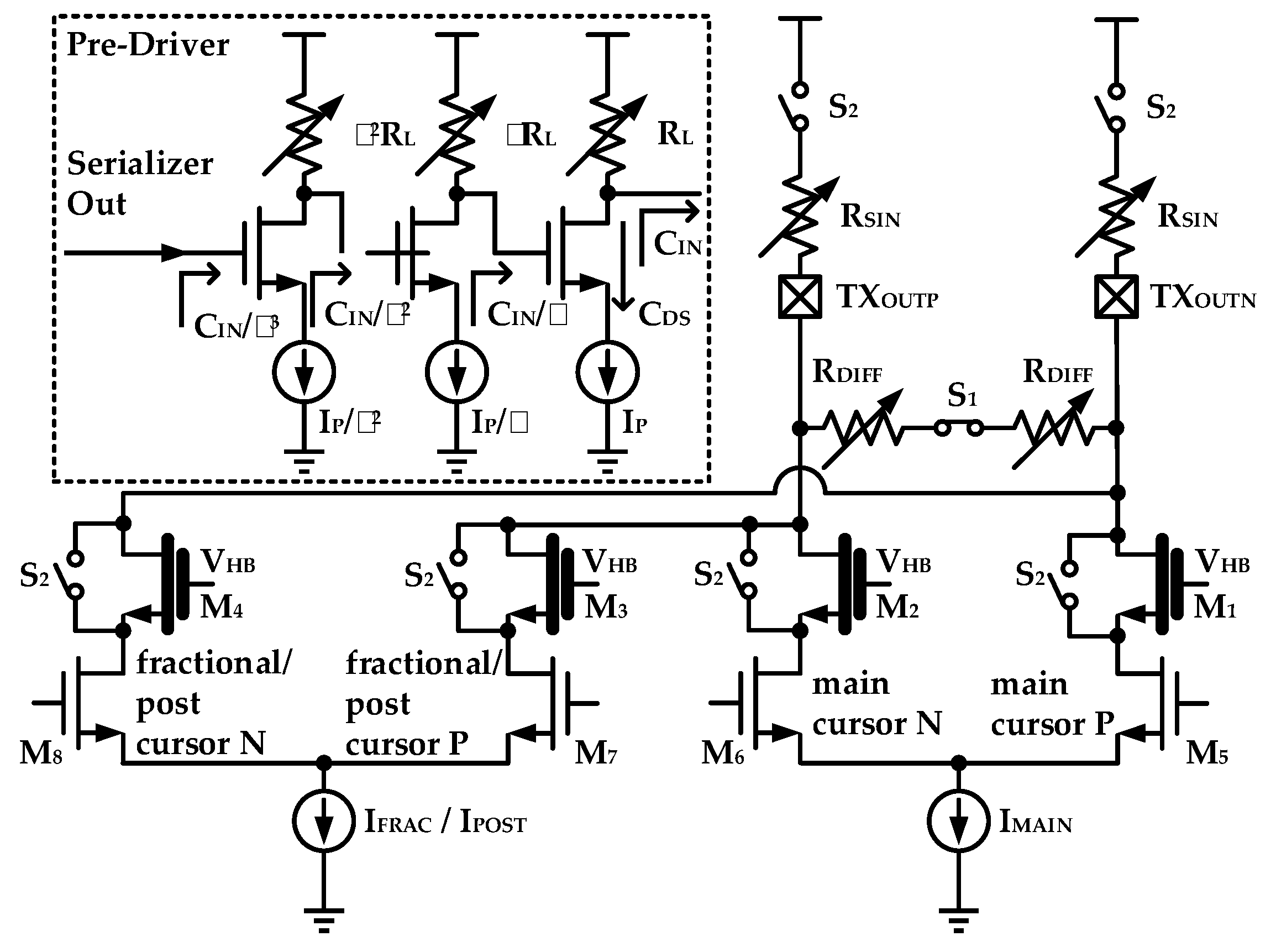
4.3.1. Predriver Circuit

An output driver circuit is required to drive a very high load. Therefore, a current mode (CM) driver needs a predriver circuit, to ensure its driving capacity. In this study, the inverse proportional method is employed to design a predriver circuit, to obtain a good trade-off between power consumption and bandwidth.

4.3.2. Reconfigurable Output Driver Circuit

A reconfigurable output driver circuit prototype, as shown in Figure 6, is designed to ensure compatibility with protocols such as High-Definition Multimedia Interface (HDMI) 2.0b and Peripheral Component Interconnect (PCI) Express 3.1. HDMI 2.0b is a relatively special protocol, in that it requires the receiver end to supply a voltage of 3.3 V and a pull-up resistor. The switches in Figure 6 are ideal, because the parasitic of the switches will degrade the performance of the driver. Satisfying the HDMI 2.0b protocol requires switches S1 to be closed and switches S2 and RSIN to be taken out. After this operation, the two differential resistors (RDIFF) connected in series serve as a 100-Ω transmission-line matching resistor, while TXOUTP and TXOUTN function as the data output end of the transmitter. As the receiver end supplies a voltage of 3.3 V, use of a conventional CM driver can lead to an overly high drain voltage for the input pair transistors, which in turn causes transistor breakdowns and circuit failure. Therefore, thick-gate transistors, M1–M4, need to be added to the input pair transistors, with the goal of reducing the drain voltage of the input transistors and preventing transistor failure.
The PCI Express 3.1 protocol requires a power supply and a pull-up resistor to be provided on chip and the data to be output below the pull-up resistor. To satisfy this protocol, it is necessary to close switches S2 and take out switches S1, RDIFF and M1–M4. This operation allows the 50-Ω RSIN to function as a pull-up resistor and a transmission-line matching resistor.

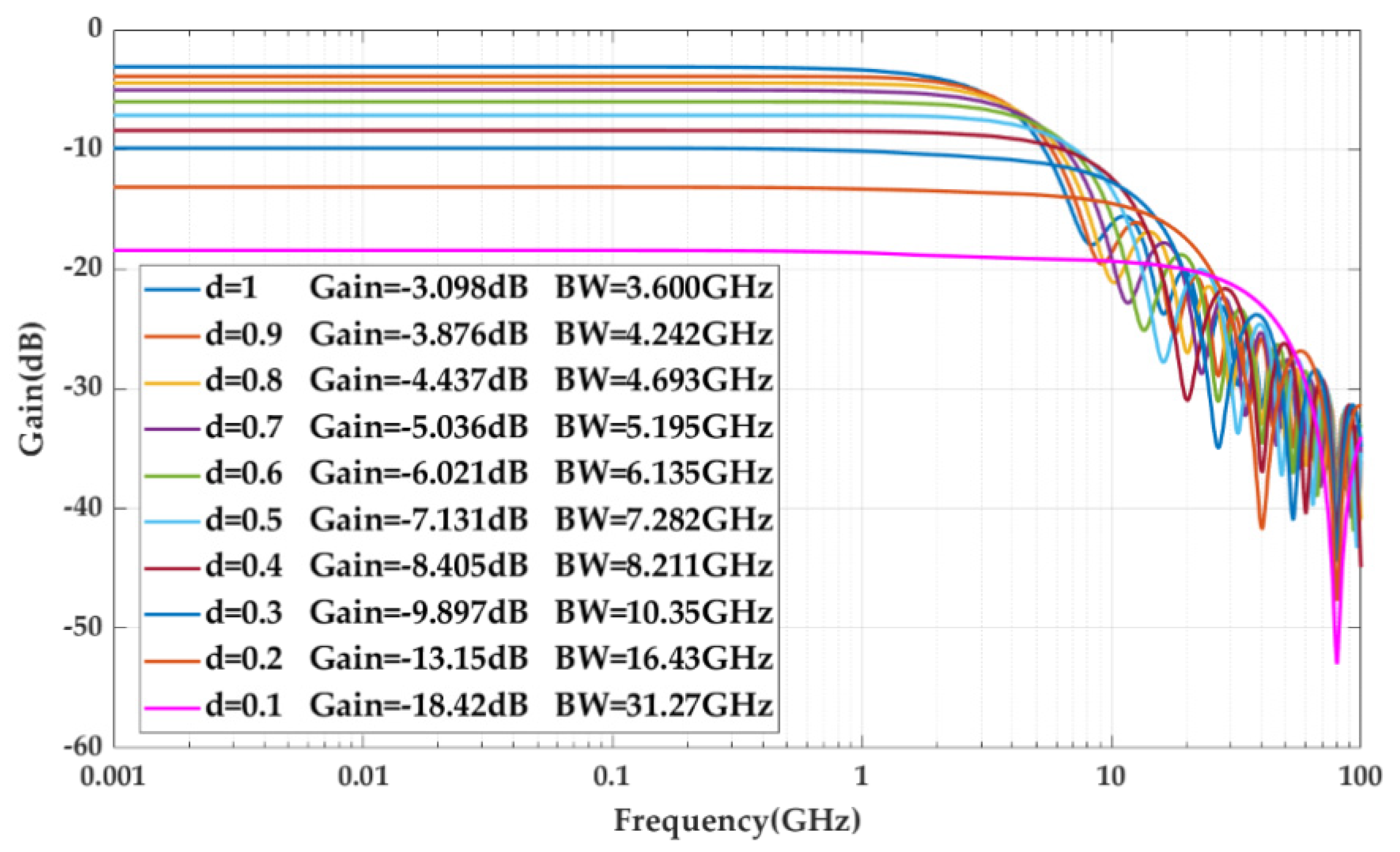
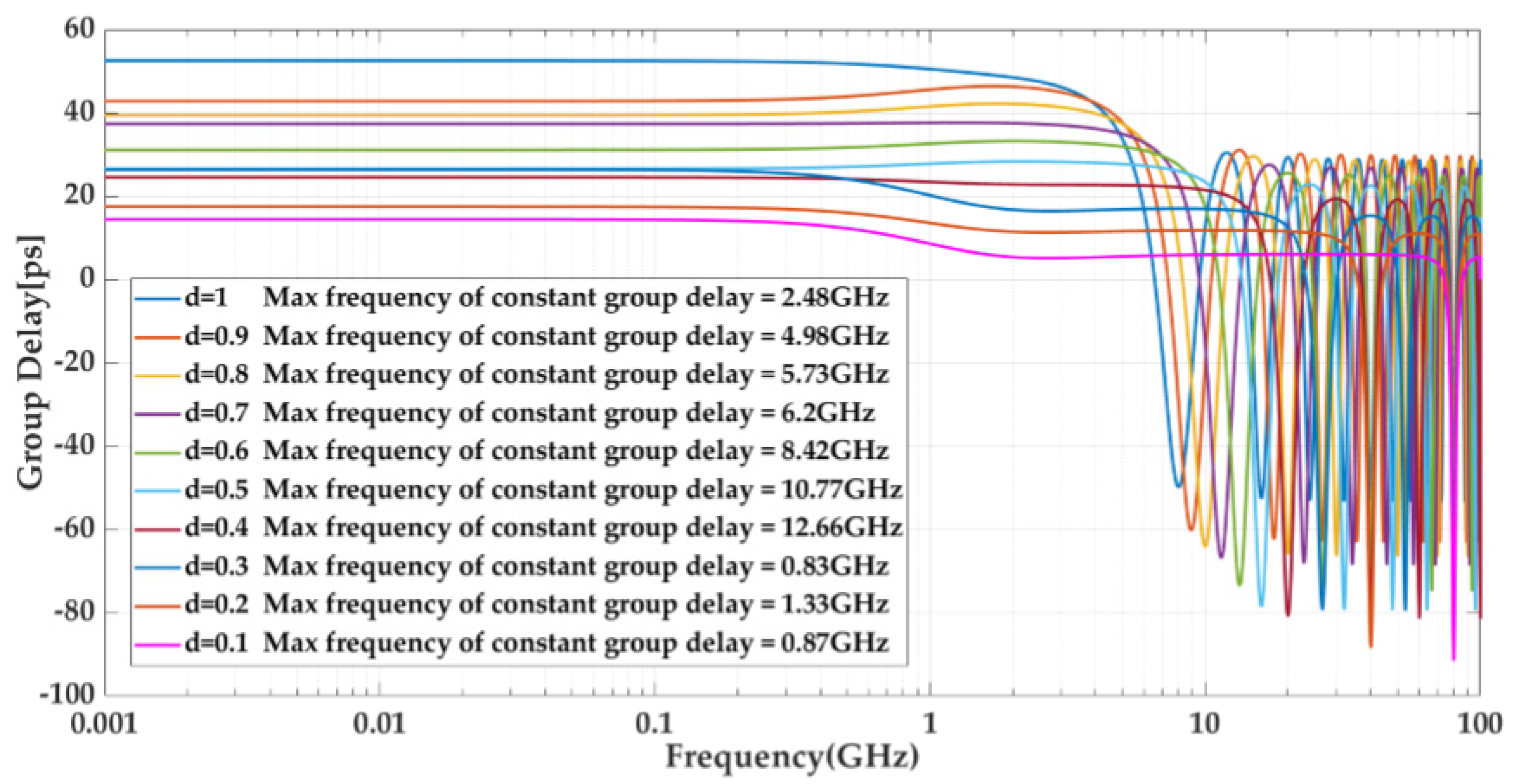
4.3.3. Three-Tap Fractional-Spaced FFE

A three-tap fractional-spaced FFE is presented for channel equalization. The three taps are the main-cursor, fractional-cursor, and post-cursor, respectively. The block diagram and the schematic of the three-tap fractional-spaced FFE are shown in Figure 7a,b, respectively, where dTUI is the delay time of the fractional-cursor relative to the main-cursor, and m is the proportion of the fractional-cursor relative to the main-cursor.
It can be ratiocinated from Figure 7 that the relationship between y(t) and x(t) is:
y ( t ) = x ( t ) m x ( t d T U I ) ,
after Laplace transformation of Equation (4), the relationship between Y(s) and X(s) in the s domain can be obtained:
H ( s ) = Y ( s ) X ( s ) = 1 m e d T U I s ,
then calculating the magnitude of H(s), we can obtain:
| H ( ω ) | = 1 + m 2 2 m cos ( d ω T U I ) .
Equation (6) shows that |H(ω)| is a periodic function for ω, and its period is 2π/(dTUI). When (dωTUI) equals π, which means ω equals π/(dTUI), |H(ω)| reaches the first maximum value, so the frequency fpeak here is:
f p e a k = 1 / ( 2 d T U I ) = f N y q u i s t / d .
Equation (7) suggests that by decreasing the coefficient d of the fractional-spaced FFE, the peak frequency of the FFE frequency response can be increased to the Nyquist frequency divided by d. Therefore, the compensable frequency can be enhanced significantly.
To verify the deduction above, a first order low-pass filter with a 3 dB bandwidth of 1.5 GHz is used to simulate the channel loss [22,23]. The bode diagram of the channel model is shown in Figure 8.
Channel equalization requires that the compensated frequency response amplitude remains flat within the band, which means it cannot be over-compensated. From this premise, the max m is chosen for different d manually. When m is smaller, the bandwidth will be degraded. When m is larger, the frequency response will introduce a peak. Hence, the m chosen for different d is the optimal value in terms of bandwidth. Therefore, each d corresponds to a specific m. Figure 9 shows the frequency response of the cascaded fractional-spaced FFE and channel.
It can be seen from Figure 9 that, as d decreases, the bandwidth of the compensated signal (BW) increases, but the low-frequency gain (Gain) decreases. Therefore, the cost of the increase in BW is the decrease in Gain. That is, in the case of the same power consumption, the bandwidth of the signal can be increased by the fractional-spaced FFE, but the output swing of the signal will be reduced.
Based on the 500 mV output swing after compensation (in the case of no attenuation, the 500 mV output swing corresponds to 5 mA pull-down current), use the ratio of BW and power consumption (set as BOP) to define the trade-off between bandwidth and power consumption corresponding to different d. The total required current at a specific d is:
I T O T A L = I M A I N + I F R A C = ( 5   mA ) 1 + m 1 m ,
where the relationship between Gain and m is:
G a i n ( dB ) = 20 log 10 ( 1 m ) .
Then combining Equations (8) and (9), the value of BOP can be obtained as:
B O P ( GHz / mA ) = B W I T O T A L = 10 ( G a i n / 20 ) ( 2 10 ( G a i n / 20 ) ) ( 5   mA ) B W .
We know that each d corresponds to a specific m, so the relationship between d, BW, and Gain is constructed. Therefore, each group of d corresponds to a specific BOP from Equation (10). Since BW and Gain should be as large as possible, the BOP should be as large as possible as well.
Based on the situation discussed above, the curve of BOP versus d is obtained, as shown in Figure 10.
This suggests that when using a fractional-spaced FFE to compensate the channel, BOP is the biggest when d is 0.5. Hence, a good compromise can be achieved between power consumption and bandwidth when d is 0.5 in this situation.
The group delay of the cascaded fractional-spaced FFE and channel with the variation of d is shown in Figure 11.
The group delay is the measure of the time delay of each frequency component of the signal passing through the system. To achieve signal transmission without distortion, the group delay should be constant. Figure 11 shows that with different d, the group delay is the constant at low frequency, and changes a lot when utilizing a higher frequency. Therefore, the max frequency of the constant group delay is set to define the degree of change of group delay with frequency. Compared with the initial constant group delay, a 5 ps variation is set to define the max frequency of constant group delay. The max frequency of constant group delay with different d is shown in Figure 11. This suggests that the fractional-spaced FFE can enhance the max frequency of the constant group delay.
Figure 12 shows the output eye diagrams with 500 mV output swing when d is 0.5 and 1, respectively. When d is 0.5, m is 0.56; while, when d is 1, d is 0.3.
Due to the increase in bandwidth, the eye height is 500 mV when d is 0.5, which is obviously better than the eye height of 370 mV when d is 1. Meanwhile, the deterministic jitter (DJ) is reduced from 4.5 to 1.5 ps. Data-dependent jitter (DDJ) is the prominent part of DJ, and DDJ is caused by threshold-crossing time deviations correlated to the previous data bits on the current data bit. As the transmitted data is produced by a particular pattern, there is insufficient bandwidth to preserve the memory of the previous data, and this will harm future data transitions [24,25]. Hence, the increased signal bandwidth will decrease DJ. As a consequence, the fractional-spaced FFE greatly improves the quality of the eye diagram and the integrity of the signal. For different channels, the BOP can be used to trade off between power consumption and output signal bandwidth, thereby compensating for different situations.
A fractional cursor is produced by the main cursor after the delay block. The block diagram of the delay block is shown in Figure 13.
The delay time is coarsely tuned by a parallel capacitor array, and finely tuned by an adjustable varactor. The delay block is placed before the single-differential converter (S2D). Compared with the case where the delay block is placed in the clock chain, the varactor diode and capacitor array used in this design are halved, which can reduce the chip area [22]. Since d is very small, the power consumption is very large, which is not conducive to a low-power design; thus, the case when d is less than 0.4 can be ignored. Under different control words of capacitance, the variation of the delay time versus Vctrl under three different PVT conditions is shown in Figure 14.
Due to the delay time variation from PVT, the effective delay time is the intersecting part of three PVT conditions, which range from 50 to 105 ps. As a result, the delay block can provide delay time ranges from 0.4 to 0.8 UI.

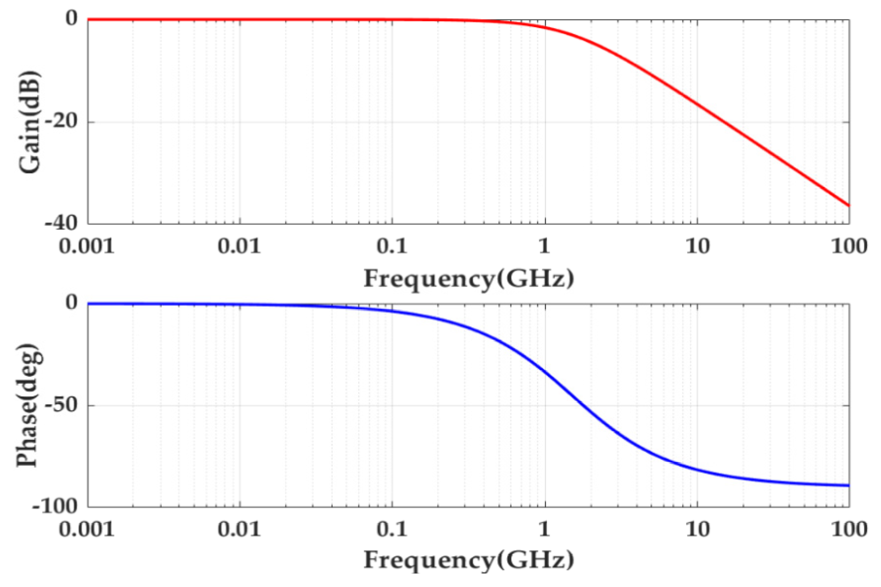
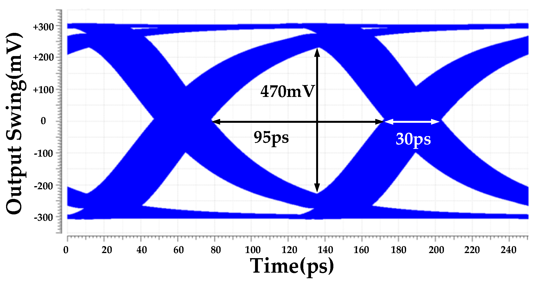
5. Simulation Results and Discussions

The designed transmitter was implemented and validated based on the SMIC-55-nm process. Figure 15 shows a photograph of the layout of the designed transmitter. The PLL and single-channel driver were 350 μm × 380 μm (0.133 mm2) and 250 μm × 300 μm (0.075 mm2) in area, respectively. Clock-shielding, virtual-device, protection-ring, and central-symmetry layout techniques were employed to implement the high-speed signal wiring and modules.
Figure 16 shows the frequency tuning range of the VCO in the PLL under three different PVT conditions. For a 8 Gbps data rate, the frequency of clock signal should be 4 GHz. Figure 16 suggests that under every PVT condition, the VCO can provide a tuning range that ranges from 1.6 to 4.6 GHz. The OD can be used to further expand the low-frequency output range and provide a broadband clock signal for the transmitter.
Figure 17 shows the phase–noise curve of the PLL at an output frequency of 4 GHz. The phase noise values of the PLL are −92 and −94 dBc/Hz at in-band frequency offsets of 100 kHz and 1 MHz, respectively, and −112 dBc/Hz at an out-of-band frequency offset of 10 MHz. The PLL exhibited a good jitter performance, as evidenced by a root-mean-square jitter of 1.93 ps in 4-GHz output clock after integration of total phase noise.
The transmitter was simulated as a whole at an operating transmission rate of 8 Gbps. In terms of power consumption, the PLL and driver consumed 27.0 and 29.2 mW of power, respectively. The 27.0 mW power consumption of the PLL includes all five LDOs. For each LDO, the power consumption was as follows: The power consumption of the LDO for VCO was 12.3 mW; the power consumption of the LDO for the second stage was 13.4 mW, which includes the power consumption of the second stage LDOs (0.9 mW for the LDO for CP, 1.8 mW for the LDO for PFD, and DIV, 4.6 mW for the LDO for OD).
Figure 18 shows the differential insertion loss curve of the line model used in the simulation. At an operating transmission rate of 8 Gbps, the Nyquist frequency and insertion loss were 4 GHz and −8.05 dB, respectively.
The transmitter was simulated with PRBS-31 code as data source. The output swing was ±300 mV. Figure 19 shows the output eye diagram of the transmitter without FFE under the typical corner, 50 °C and 1.2 V supply. The excessive inter-symbol interference resulted in a highly distorted eye diagram.
Figure 20 shows the output eye diagram of the transmitter equipped with baud-spaced FFE under typical corner, 50 °C and 1.2 V supply. The eye height is 340 mV. Here, a bit error ratio lower than 10−12 is used as a criterion. In total, the PLL introduces a jitter of 28 ps. The eye width of the eye diagram of the whole transmitter is 0.69 UI.
Figure 21 shows the output eye diagram of the transmitter equipped with a fractional-spaced FFE under a typical corner, 50 °C and 1.2 V supply. The eye height and the eye width of the output data were 470 mV and 0.76 UI, respectively. Due to the enhancement of bandwidth by the fractional-spaced FFE, under the same output swing, the eye height was increased by 130 mV, and the total jitter was decreased by 8 ps. The verification results show the effectiveness and feasibility of the proposed fractional-spaced FFE.
Table 1 compares the eye height and eye width of the transmitter output data compensated by the fractional-spaced FFE under nine different PVT conditions. The valid eye height is at least 0.68, due to the attenuation of MOSFET speed caused by the slow corner, 125 °C and 1.08 V supply. The eye width is at least 0.71 UI without much change, because the jitter is mainly caused by the RJ introduced by the PLL.
Table 2 compares the transmitter presented in this paper with recent transmitters that were fabricated with a similar CMOS technology and operating at a similar data rate. The transmitter in this article has a relatively low power consumption. Meanwhile, the proposed transmitter outputs data with low jitter. Moreover, this paper proposes a three-tap fractional-spaced FFE to equalize the channel loss, which can notably increase the valid eye height.

6. Conclusions

An 8-Gbps, low-jitter, four-channel transmitter equipped with a three-tap fractional-spaced FFE was designed in this study. The PLL can provide a differential clock with high speed and low jitter. A 32-to-1 MUX was also designed to serialize 32-bit data. Moreover, a novel FDC architecture was developed to satisfy the time requirements for high-speed data serialization, with applicability for higher-speed transmitter architectures. A reconfigurable output driver was put forward, to ensure compatibility with multiple protocols. Finally, a three-tap fractional-spaced FFE was employed to compensate for channel loss. The fractional-spaced FFE can overcome the shortcoming that the peak frequency of the baud-spaced FFE frequency response can only reach the Nyquist frequency; hence, it can enhance the signal bandwidth observably, thereby improving signal integrity and performance. The validation results showed that the PLL can provide differential clock up to 4 GHz, and the RJ is 1.93 ps at this rate; therefore, the jitter performance is good. At 8-Gbps, PRBS-31 was used as data source to simulate the whole transmitter. The energy efficiency of the driver stage was 3.65 mW/Gbps. Moreover, the fractional-spaced FFE could effectively improve the signal integrity of the output data. After channel compensation through FFE, the eye width and valid eye height of the output data were 0.71 UI and 0.68, respectively.

Author Contributions

Circuits design and simulation, Y.H. and H.Y.; investigation, Y.H.; methodology, Y.H.; software, Z.Y.; writing—original draft, Y.H.; writing—review and editing, Y.H., H.Y., W.C. and S.Q. All authors have read and agreed to the published version of the manuscript.

Funding

This research received no external funding.

Conflicts of Interest

The authors declare no conflict of interest.

References

  1. Choi, Y.H.; Seong, K.; Kim, B.; Sim, J.Y.; Park, H.J. All-synthesizable 6Gbps voltage-mode transmitter for serial link. In Proceedings of the 2016 IEEE Asian Solid-State Circuits Conference (A-SSCC), Toyama, Japan, 7–9 November 2016; IEEE: Toyama, Japan, 2016; pp. 245–248. [Google Scholar]
  2. Hyun, C.; Ko, H.; Chae, J.H.; Park, H.; Kim, S. A 20Gb/s dual-mode PAM4/NRZ single-ended transmitter with RLM compensation. In Proceedings of the 2019 IEEE International Symposium on Circuits and Systems (ISCAS), Sapporo, Japan, 26–29 May 2019; IEEE: Sapporo, Japan, 2019; pp. 1–4. [Google Scholar]
  3. Ma, S.; Yu, H.; Gu, Q.J.; Ren, J. A 5–10-Gb/s 12.5-mW source synchronous I/O interface with 3-D flip chip package. IEEE Trans. Circuits Syst. I Regul. Pap. 2018, 66, 555–568. [Google Scholar] [CrossRef]
  4. Kwon, D.H.; Kim, M.; Kim, S.G.; Choi, W.Y. A low-power 40-Gb/s pre-emphasis PAM-4 transmitter with toggling serializers. IEEE Trans. Circuits Syst. II Express Br. 2020, 67, 430–434. [Google Scholar] [CrossRef]
  5. Wang, Z.; Choi, M.; Lee, K.; Park, K.; Liu, Z.; Biswas, A.; Han, J.; Du, S.; Alon, E. An Output Bandwidth Optimized 200-Gb/s PAM-4 100-Gb/s NRZ Transmitter With 5-Tap FFE in 28-nm CMOS. IEEE J. Solid-State Circuits 2021, 57, 21–31. [Google Scholar] [CrossRef]
  6. Geng, X.; Tian, Y.; Xiao, Y.; Ye, Z.; Xie, Q.; Wang, Z. A 25.8 GHz integer-N PLL with time-amplifying phase-frequency detector achieving 60 fs rms jitter, −52.8 dB FoM J, and Robust lock acquisition performance. In Proceedings of the 2022 IEEE International Solid- State Circuits Conference (ISSCC), San Francisco, CA, USA, 20–26 February 2022; IEEE: San Francisco, CA, USA, 2022; pp. 388–390. [Google Scholar]
  7. Sun, D.; Ding, R.; Bu, F.; Lu, S.; Liang, H.; Zhou, R.; Liu, S.; Zhu, Z. A Type-II Dual-Path PLL With Reference-Spur Suppression. IEEE Trans. Microw. Theory Tech. 2022, 70, 2280–2289. [Google Scholar] [CrossRef]
  8. Cai, C.; Zheng, X.; Chen, Y.; Wu, D.; Luan, J.; Lu, D.; Zhou, L.; Wu, J.; Liu, X. A 1.55-to-32-Gb/s four-lane transmitter with 3-tap feed forward equalizer and shared PLL in 28-nm CMOS. Electronics 2021, 10, 1873. [Google Scholar] [CrossRef]
  9. Bandarupalli, J.D.; Gautam, R.; Saxena, S. A reconfigurable 0.1–10 Gb/s voltage-mode transmitter with 0.2–1 V output swing. IEEE Solid State Circuits Lett. 2019, 2, 53–56. [Google Scholar] [CrossRef]
  10. Wang, T.; Zhou, M.; Liu, J.; Wang, Z.; Mo, J.; Chen, H.; Yu, F. A highly linear 10 Gb/s MOS current mode logic driver with large output voltage swing based on an active inductor. IEICE Electron. Express 2020, 17, 20200160. [Google Scholar] [CrossRef]
  11. Bai, X.; Zhao, J.; Zuo, S.; Zhou, Y. A 1.89 mW/Gbps SST transmitter with three-tap FFE and impedance calibration. IEICE Electron. Express 2019, 16, 20190356. [Google Scholar] [CrossRef] [Green Version]
  12. Norimatsu, T.; Kogo, K.; Komori, T.; Kohmu, N.; Yuki, F.; Kawamoto, T. A 100-Gbps 4-lane transceiver for 47-dB loss copper cable in 28-nm CMOS. IEEE Trans. Circuits Syst. I Regul. Pap. 2020, 67, 3433–3443. [Google Scholar] [CrossRef]
  13. Peng, P.J.; Chen, Y.T.; Lai, S.T.; Huang, H.E. A 112-Gb/s PAM-4 Voltage-Mode Transmitter With Four-Tap Two-Step FFE and Automatic Phase Alignment Techniques in 40-nm CMOS. IEEE J. Solid-State Circuits 2020, 56, 2123–2131. [Google Scholar] [CrossRef]
  14. Momtaz, A.; Green, M.M. An 80 mW 40 Gb/s 7-tap T/2-spaced feed-forward equalizer in 65 nm CMOS. IEEE J. Solid-State Circuits 2010, 45, 629–639. [Google Scholar] [CrossRef]
  15. Dickson, T.O.; Ainspan, H.A.; Meghelli, M. A 1.8 pJ/b 56Gb/s PAM-4 transmitter with fractionally spaced FFE in 14nm CMOS. In Proceedings of the 2017 IEEE International Solid-State Circuits Conference (ISSCC), San Francisco, CA, USA, 5–9 February 2017; pp. 118–119. [Google Scholar]
  16. Guo, R.; Lu, Z.; Hu, S.; Yu, Q.; Rong, L.; Liu, Y. Design and verification of a charge pump in local oscillator for 5G applications. Electronics 2021, 10, 1009. [Google Scholar] [CrossRef]
  17. Chen, J.; Zhang, W.; Sun, Q.; Liu, L. An 8–12.5-GHz LC PLL with dual VCO and noise-reduced LDO regulator for multilane multiprotocol SerDes in 28-nm CMOS technology. Electronics 2021, 10, 1686. [Google Scholar] [CrossRef]
  18. Zou, W.; Ren, D.; Zou, X. A wideband low-jitter PLL with an optimized ring-VCO. IEICE Electron. Express 2020, 17, 20190703. [Google Scholar] [CrossRef] [Green Version]
  19. Chen, Y.; Gong, J.; Staszewski, R.B.; Babaie, M. A fractional-N digitally intensive PLL achieving 428-fs jitter and <-54-dBc spurs under 50-mVpp supply ripple. IEEE J. Solid-State Circuits 2021, 57, 1749–1764. [Google Scholar] [CrossRef]
  20. Park, K.; Oh, T. 12 Gbit/s three-tap FFE half-rate transmitter with low jitter clock buffering scheme. Electron. Lett. 2019, 55, 1078–1080. [Google Scholar] [CrossRef]
  21. Fiedler, A.; Krishnan, S. A scalable 7.0-Gb/s multi-lane NRZ transceiver with a 1/10th-rate forwarded clock in 0.13 um CMOS. In Proceedings of the 2016 IEEE International Symposium on Circuits and Systems (ISCAS), Montreal, QC, Canada, 1 May 2016; pp. 2330–2333. [Google Scholar]
  22. Zheng, X.; Ding, H.; Zhao, F.; Wu, D.; Zhou, L.; Wu, J.; Lv, F.; Wang, J.; Liu, X. A 50–112-Gb/s PAM-4 transmitter with a fractional-spaced FFE in 65-nm CMOS. IEEE J. Solid-State Circuits 2020, 55, 1864–1876. [Google Scholar] [CrossRef]
  23. Ding, H.; Zheng, X.; Wu, D.; Zhou, L.; Wu, J.; Lv, F.; Wang, J.; Liu, X. A 112-Gb/s PAM-4 Transmitter With a 2-Tap Fractional-Spaced FFE in 65-nm CMOS. IEEE Solid State Circuits Lett. 2019, 2, 195–198. [Google Scholar] [CrossRef]
  24. Buckwalter, J.F.; Hajimiri, A. Analysis and equalization of data-dependent jitter. IEEE J. Solid-State Circuits 2006, 41, 607–620. [Google Scholar] [CrossRef] [Green Version]
  25. Yoon, K.; Park, H.; Choi, Y.; Sim, J.; Choi, J.; Kim, C. A 4.5 Gb/s/pin transceiver with hybrid inter-symbol interference and far-end crosstalk equalization for next-generation high-bandwidth memory interface. Electron. Lett. 2022, 58, 420–422. [Google Scholar] [CrossRef]
Figure 1. Block diagram of transmitter architecture.
Electronics 11 01768 g001
Figure 2. Block diagram of the PLL architecture.
Electronics 11 01768 g002
Figure 3. Block diagram of the 32-to-1 MUX architecture.
Electronics 11 01768 g003
Figure 4. Block diagram of 2-to-1 MUX architecture.
Electronics 11 01768 g004
Figure 5. (a) The architecture and (b) timing diagram of FDC.
Electronics 11 01768 g005
Figure 6. Schematic of the output driver.
Electronics 11 01768 g006
Figure 7. (a) Block diagram and (b) schematic of the three-tap fractional-spaced FFE.
Electronics 11 01768 g007
Figure 8. Bode diagram of the channel model.
Electronics 11 01768 g008
Figure 9. Frequency response of the cascaded fractional-spaced FFE and channel.
Electronics 11 01768 g009
Figure 10. Normalized BOP versus the variation of d.
Electronics 11 01768 g010
Figure 11. Group delay of the cascaded fractional-spaced FFE and channel.
Electronics 11 01768 g011
Figure 12. Comparison of eye diagram when d is 0.5 and 1.
Electronics 11 01768 g012
Figure 13. Block diagram of delay block.
Electronics 11 01768 g013
Figure 14. The delay time tuning range under (a) fast corner, −25 °C, and 1.32 V supply; (b) typical corner, 50 °C, and 1.2 V supply; (c) slow corner, 125 °C, and 1.08 V supply.
Electronics 11 01768 g014
Figure 15. Layout of the transmitter.
Electronics 11 01768 g015
Figure 16. Tuning range of the VCO under (a) fast corner, −25 °C, and 3.63 V supply; (b) typical corner, 50 °C, and 3.3 V supply; (c) slow corner, 125 °C, and 2.97 V supply.
Electronics 11 01768 g016
Figure 17. Phase-noise curve of the PLL.
Electronics 11 01768 g017
Figure 18. Differential insertion loss curve of the cable model.
Electronics 11 01768 g018
Figure 19. Output eye diagram without FFE.
Electronics 11 01768 g019
Figure 20. Output eye diagram with baud-spaced FFE.
Electronics 11 01768 g020
Figure 21. Output eye diagram with fractional-spaced FFE.
Electronics 11 01768 g021
Table 1. Comparison of the valid eye height and eye width with fractional-spaced FFE under nine PVT conditions.
ProcessSupply Voltage (V)Temperature (°C)Valid Eye Height 1Eye Width (UI)
Typical −250.810.76
1.2500.780.76
1250.740.74
Fast −250.830.77
1.32500.790.76
1250.780.76
Slow −250.750.72
1.08500.720.72
1250.680.71
1 Valid eye height = eye height/output swing.
Table 2. Performance comparison and summary.
This Work 1[1] 2[2] 2[9] 2[11] 2
CMOS Technology (nm)5565656555
Data Rate (Gbps)8610108
Power 3 (mW)29.233.672.036.015.1
Energy Efficiency 4 (mW/Gbps)3.655.607.203.601.89
Eye Width0.710.650.700.580.52
Valid Eye Height0.680.320.630.350.52
FFE Tap32423
Type of FFEFractional-spacedBaud-spacedBaud-spacedBaud-spacedBaud-spaced
1 Simulated result. 2 Measured result. 3 The power is for a single lane of the transmitter. 4 Energy Efficiency (mW/Gbps) = Power/Data Rate.
Publisher’s Note: MDPI stays neutral with regard to jurisdictional claims in published maps and institutional affiliations.

