Article

A Compact Transformer-Based E-Band CMOS Power Amplifier with Enhanced Efficiencies of 15.6% PAE1dB and 6.5% PAE at 6 dB Power Back-Off

1
School of Information Science and Engineering, Southeast University, Nanjing 210096, China
2
School of Cyber Science and Engineering, Southeast University, Nanjing 210096, China
3
S-TEK Research Center, Shanghai 201203, China
*
Author to whom correspondence should be addressed.
Electronics 2022, 11(11), 1679; https://doi.org/10.3390/electronics11111679
Submission received: 10 May 2022 / Revised: 22 May 2022 / Accepted: 23 May 2022 / Published: 25 May 2022

Abstract

:
This paper presents a compact E-band power amplifier (PA) implemented in a 40 nm CMOS process. The neutralization technique is adopted to improve reverse isolation, stability and power gain. The linearity of the PA is improved by operating the output stage in the deep class-AB region. Transformer-based matching networks (TMNs) are used for impedance transformation, and optimized for output power and efficiency. At 81 GHz, the presented PA achieves a maximum output 1 dB compressed power (P1dB) of 11.2 dBm and a saturated output power (Psat) of 12.7 dBm with 1 V supply. The power-added efficiencies at P1dB (PAE1dB) and 6 dB power back-off (PBO) are 15.6% and 6.5%, respectively.

1. Introduction

Driven by the exponential increase in data traffic, millimeter-wave frequency bands of 57–66 GHz, 71–76 GHz and 81–86 GHz have been proposed for 5G communication owing to their large available bandwidth [1,2]. Several types of E-band RF circuits have been reported [3,4,5,6], and the high-efficiency power amplifier (PA) is an essential component in the transmitter. High-order modulation schemes with a high peak-to-average power ratio (PAPR) are employed to realize higher data rates. In order to preserve signal integrity and linearity, PA has to operate in power back-off (PBO) mode [5,6].
High output 1 dB compressed power (P1dB) and power-added efficiency at P1dB (PAE1dB) are among the major difficulties for the PA design, due to the lossy substrate, low supply voltage, and low gain of transistors based on the CMOS process at millimeter-wave frequencies [7]. The power-combining technique has been proposed to achieve a higher output power [8,9,10] with the drawback of degraded efficiency.
Doherty [11], outphasing [12] and balanced structures [13] have been proposed to improve PA linearity. In [11], a transformer-based Doherty PA at the E-band is presented with a P1dB of 19.2 dBm and a PAE1dB of 12.4% at 1.5 V supply voltage. A 60 GHz transmitter incorporating an outphasing PA is proposed in [12], achieving 12.5 dBm average output power and 15% average PAE. A class-F balanced power amplifier with input and output couplers is proposed in [13] to improve the linearity and efficiency; however, PAs based on the above design schemes require complex output matching networks, leading to a larger chip area.
Power amplifiers with P1dB close to the saturated power (Psat) are preferred for power performance in the PBO mode [6]. Recently, several compact PA structures with a high saturated output power have been implemented [2,3,5], yet they suffer from soft saturation with P1dB severely lower than Psat, with a P1dB/Psat ratio about 75% in dBm [2].
In this paper, we present a compact E-band CMOS PA with high efficiency and P1dB close to Psat. The transformer-based matching networks (TMNs) are used for impedance transformation and optimized for output power and efficiency. Fabricated in the 40 nm CMOS process, the presented PA achieves 11.2 dBm P1dB and 12.7 dBm Psat, with a P1dB/Psat ratio of 88% in dBm. The power-added efficiencies at P1dB and 6 dB PBO are 15.6% and 6.5%, respectively.
This paper is organized as follows. Section 2 presents the topology of the PA. Section 3 provides the theoretical analyses and design considerations for the TMNs. Section 4 presents the measurement results of the presented PA, and Section 5 concludes the paper.

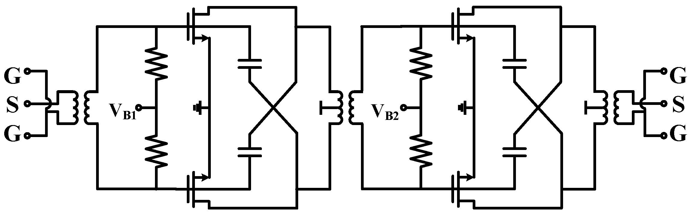
2. E-Band PA Circuit Topology

The schematic of the presented single-path PA is illustrated in Figure 1. Each stage employs a common-source pseudo-differential pair with neutralization capacitors [14]. The gate of the common-source stage is biased through resistors to improve the common-mode stability of the amplifier [8]. The neutralization capacitors in the PA are implemented with mimcap. The driver stage is sized down by a factor of two to provide sufficient driving power to the output stage. On-chip transformers are used to perform desired impedance transformations in the output and inter-stage matching networks. The common-mode gain of the differential pair is reduced by using bypass capacitors (not shown in Figure 1) to improve the common-mode stability.
Figure 2 shows the simulation results of P1dB, Psat, and the gain of the output and driver stages versus the transistor current density. Psat and gain of the output stage both increase as the current density increases, while a valley exists in the P1dB curve. The difference between the P1dB and Psat of the output stage can be reduced when the transistors are biased in the deep Class-AB region with a current density lower than 30 μA/μm. This is due to the internal harmonic cancelations of the deep Class-AB operation, which forms a minimum linear point when the output power increases close to Psat [15]. To compensate the gain degradation of the output stage, the driver stage is biased for a high gain.

3. PA Circuit Design with Transformer-Based Matching Network

To improve output power and efficiency, the output and inter-stage matching networks are designed to provide optimal load impedances for the transistors they are connected to [7]. The circuit design and parameter optimization are carried out with the guidance of following impedance formulations and demonstrated by the output matching network.

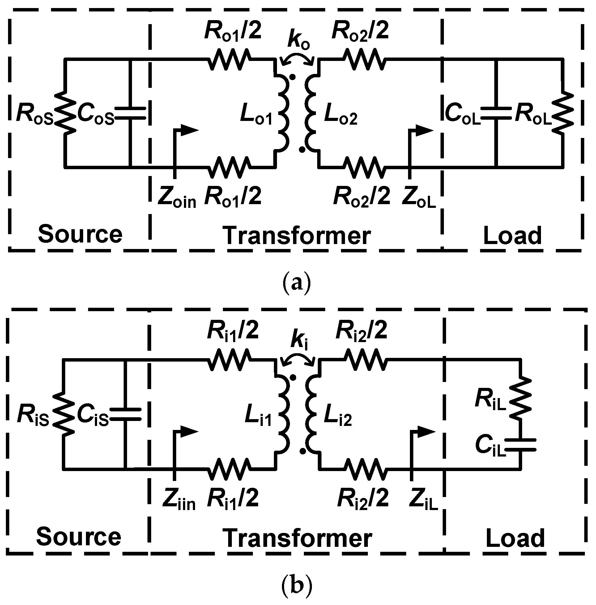
3.1. Impedance Formulations for TMN

The circuit model of the TMN for output matching is illustrated in Figure 3a, where ko is the magnetic coupling coefficient and Lo1 and Lo2 are the transformer inductances. Ro1 and Ro2 are the transformer parasitic resistances. The source of the output matching network is the output impedance of the output stage, which can be simplified as resistance RoS and capacitance CoS in parallel. The above circuit model can also be applied to the load in the output matching network, as well as the source in the inter-stage matching network.
The TMN circuit model for inter-stage matching is illustrated in Figure 3b, where ki is the magnetic coupling coefficient, Li1 and Li2 are the transformer inductances, and Ri1 and Ri2 are the transformer parasitic resistances. The source of the inter-stage matching network is modeled as resistance RiS and capacitance CiS in parallel, and the load is the input impedance of the output stage, which can be represented by resistance RiL and capacitance CiL in series.
An optimal load impedance is required at the transistor-cell output to achieve a larger output power and higher power-added efficiency. As the source capacitance and resistance are retrieved according to the load–pull characteristics of the transistor cell, the design target for the output matching network is equivalent to achieving Zoin = Zoopt, where Zoin is the input impedance of the transformer in the TMN for output matching and Zoopt is the optimal load impedance of the output stage.
The load of the output matching network is modeled as capacitance CoL and resistance RoL in parallel; thus, Zoin becomes:
Z oin = R o 1 + ω 2 k o 2 L o 1 L o 2 ( ω 2 R o 2 R oL 2 C oL 2 + R o 2 + R oL ) ( R o 2 + R oL ω 2 C oL R oL L o 2 ) 2 + ω 2 ( C oL R oL R o 2 + L o 2 ) 2 + j ω [ L o 1 + ω 2 k o 2 L o 1 L o 2 ( C oL R oL 2 L o 2 ω 2 C oL 2 R oL 2 L o 2 ) ( R o 2 + R oL ω 2 C oL R oL L o 2 ) 2 + ω 2 ( C oL R oL R o 2 + L o 2 ) 2 ]
Lo1 and ko can be obtained according to Zoin = Zoopt:
L o 1 = Im [ Z oopt ] ω ( Re [ Z oopt ] R o 1 ) C oL R oL 2 L o 2 ω 2 C oL 2 R oL 2 L o 2 ω 2 R o 2 R oL 2 C oL 2 + R o 2 + R oL
k o = ( Re [ Z oopt ] R o 1 ) ( R o 2 + R oL ω 2 C oL R oL L o 2 ) 2 + ω 2 ( C oL R oL R o 2 + L o 2 ) 2 ω 2 L o 1 L o 2 ( ω 2 R o 2 R oL 2 C oL 2 + R o 2 + R oL )
Equations (2) and (3) provide the values for Lo1 and ko as a function of Lo2, which can serve as a guideline for the design of transformer layout in the output matching network. Transformer layouts can be simulated using a 3D electromagnetic (EM) simulator.
The design target for the inter-stage matching network is equivalent to achieving Ziin = Zdopt, where Ziin is the input impedance of the transformer in the TMN for inter-stage matching, and Zdopt is the optimal load impedance of the driver stage.
The load of the inter-stage matching network is modeled as resistance RiL and capacitance CiL in series; thus, Ziin becomes:
Z iin = R i 1 + ω 4 k i 2 L i 1 L i 2 C iL 2 ( R i 2 + R iL ) ω 2 C iL 2 ( R i 2 + R iL ) 2 + ( ω 2 C iL L i 2 1 ) 2 + j ω [ L i 1 + ω 2 k i 2 L i 1 L i 2 C iL ( 1 ω 2 C iL L i 2 ) ω 2 C iL 2 ( R i 2 + R iL ) 2 + ( ω 2 C iL L i 2 1 ) 2 ]
Li1 and ki can be obtained according to Ziin = Zdopt:
L i 1 = Im [ Z dopt ] ω ( Re [ Z dopt ] R i 1 ) ω 2 k i 2 L i 1 L i 2 C iL ( 1 ω 2 C iL L i 2 ) ω 4 k i 2 L i 1 L i 2 C iL 2 ( R i 2 + R iL )
k i = ( Re [ Z dopt ] R i 1 ) ω 2 C iL 2 ( R i 2 + R iL ) 2 + ( ω 2 C iL L i 2 1 ) 2 ω 4 L i 1 L i 2 C iL 2 ( R i 2 + R iL )

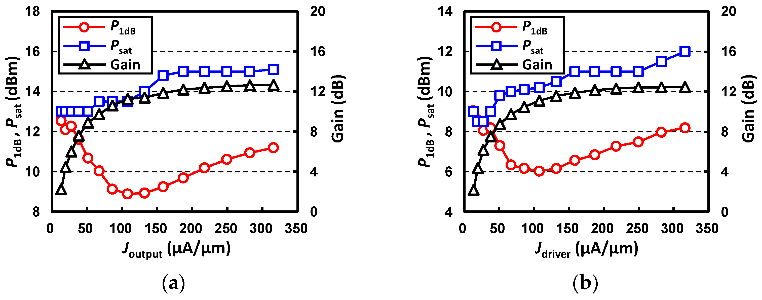
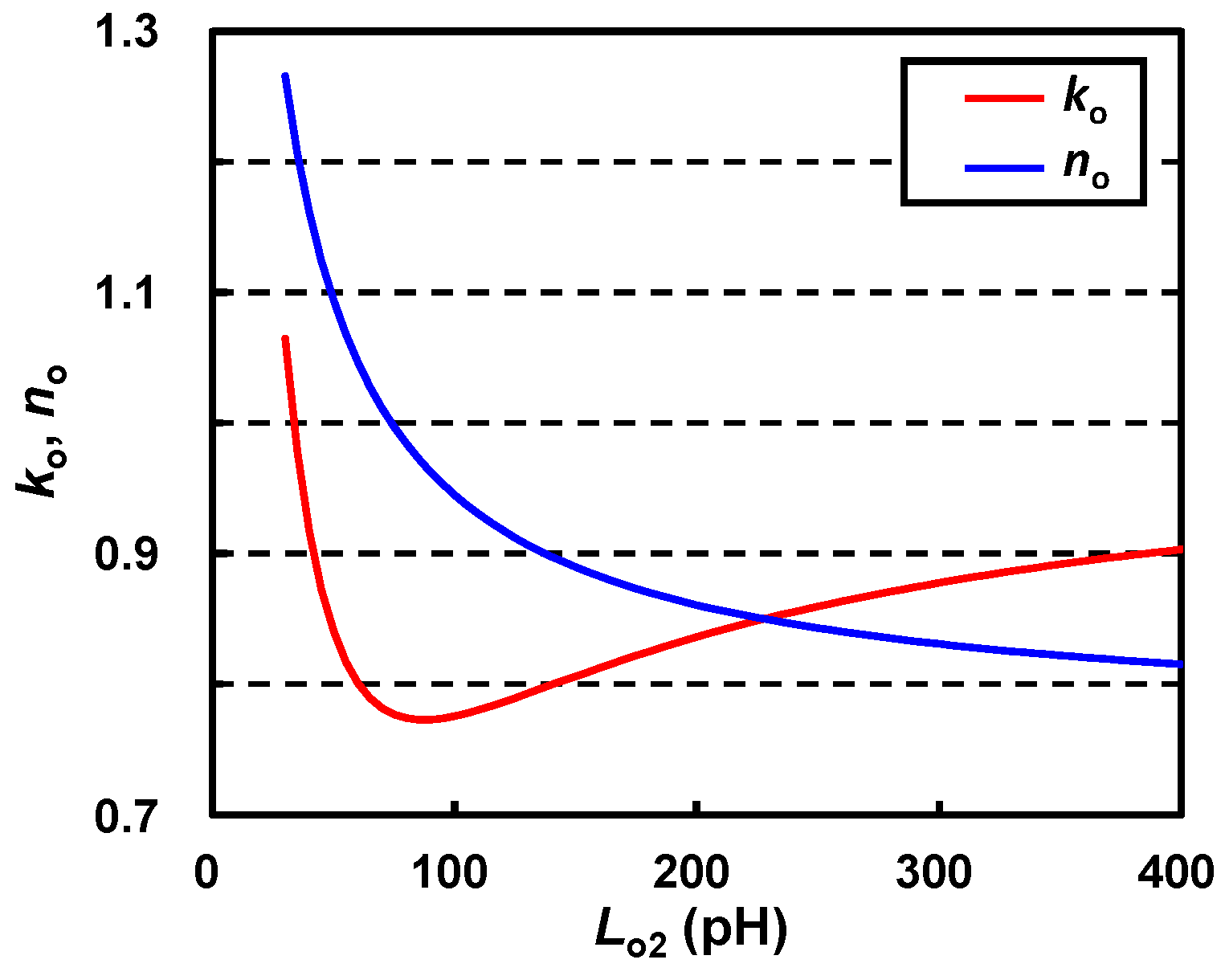
3.2. Design of Output Matching Network

According to Equations (2) and (3), the calculation of Lo1 and ko requires the knowledge of load capacitance CoL and resistance RoL, as well as parasitic resistances Ro1 and Ro2. CoL and RoL can be calculated based on the EM simulation of output GSG pads. As the transformer windings are usually implemented with the top two metal layers to reduce insertion loss, the typical values of Ro1 and Ro2 are usually assumed to be 1 Ω and 1.5 Ω, respectively.
The optimal load impedance of the output stage can be derived by load–pull analysis. In our design, Zoopt is (16.5 + j21.1) Ω at 81 GHz. According to Equations (2) and (3), the calculated ko and no for Lo2 ranging from 30 to 400 pH are shown in Figure 4, where no is the turn ratio and defined as n o = L o 2 / L o 1 . When Lo2 is selected to be 70 pH, the calculated turn ratio no is 1.03 and the magnetic coupling coefficient ko is 0.78.
The top two metal layers are used to construct the transformer windings, and the selected parameters Lo2, ko and no are realized by adjusting the transformer dimensions.

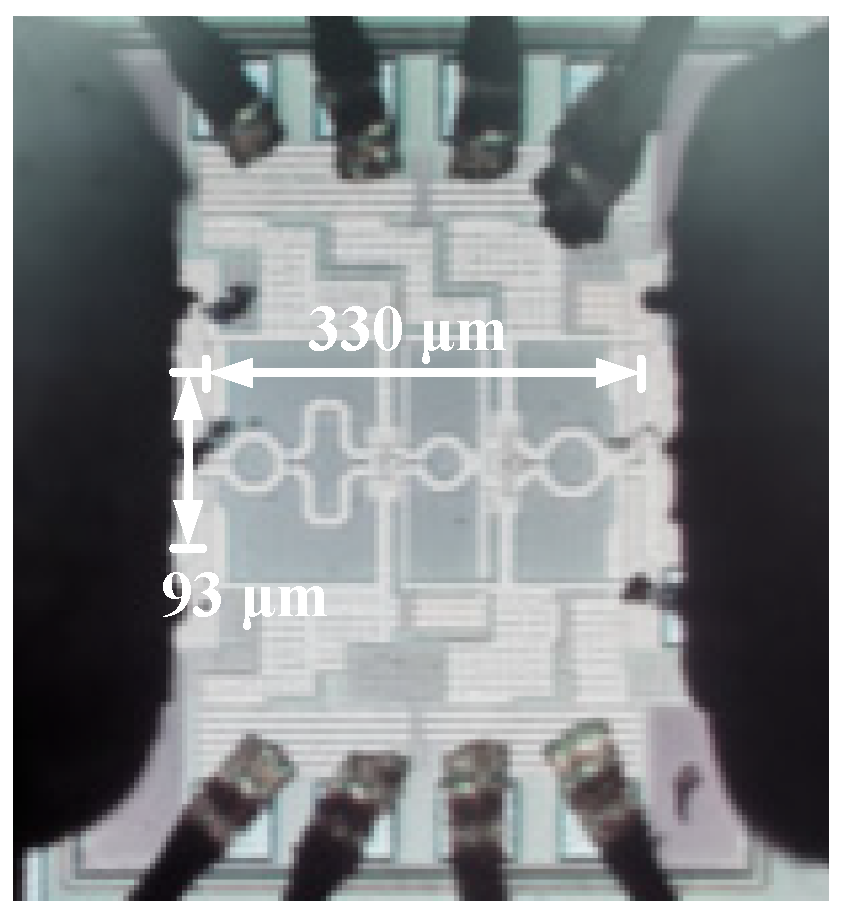
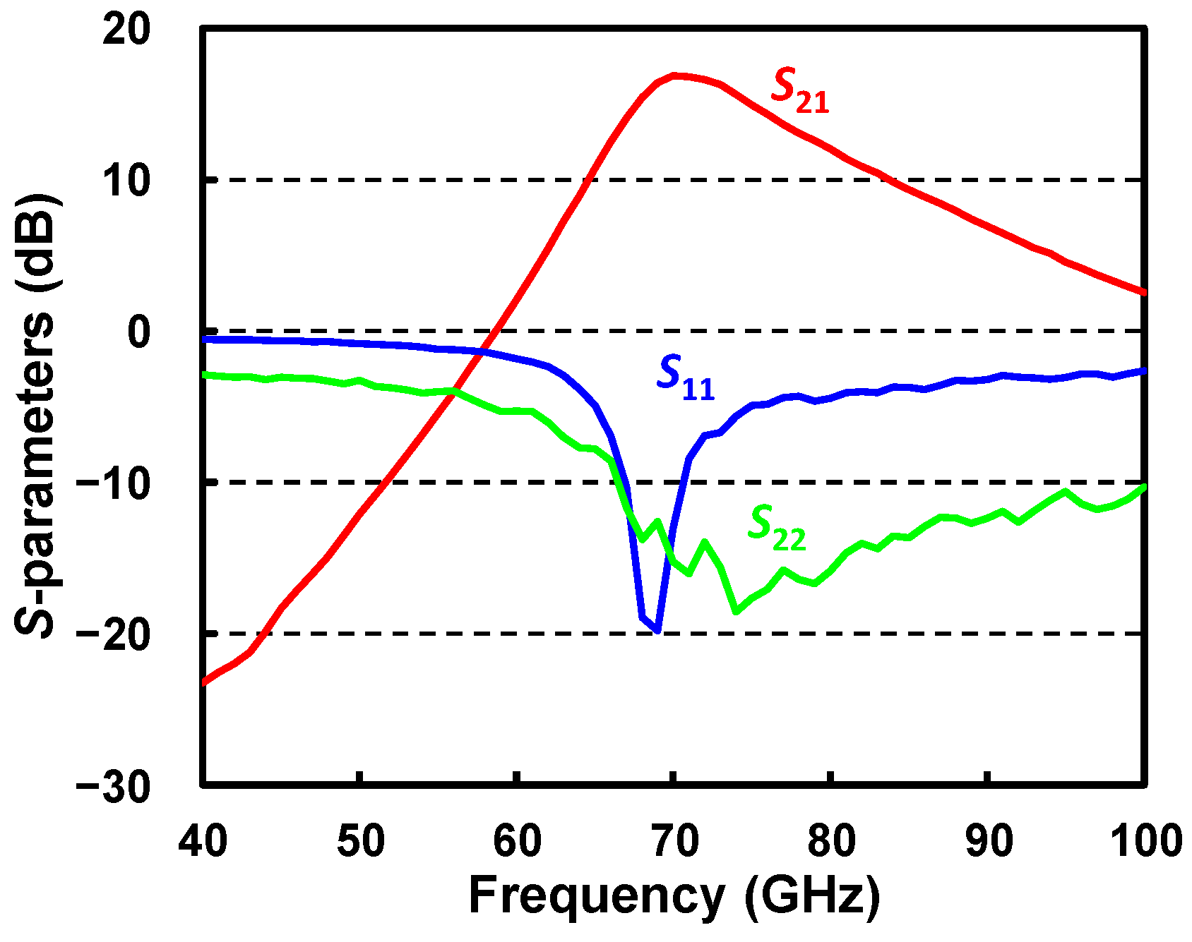
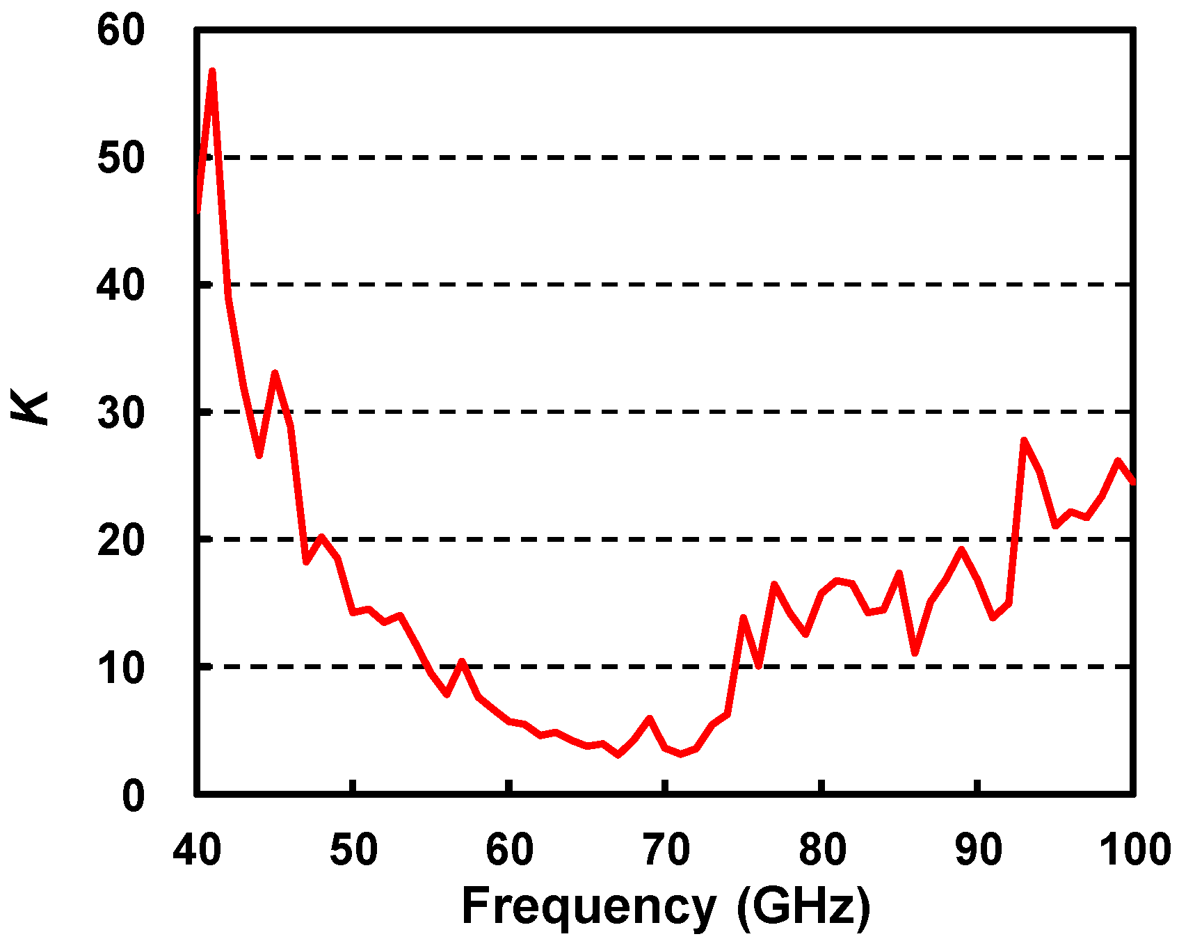
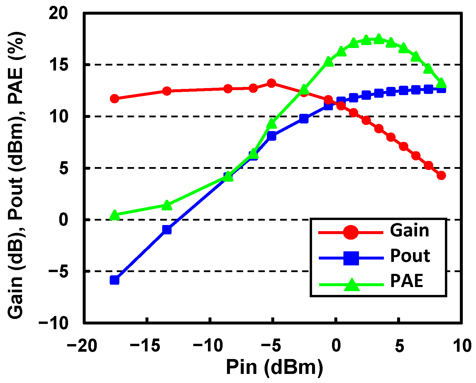
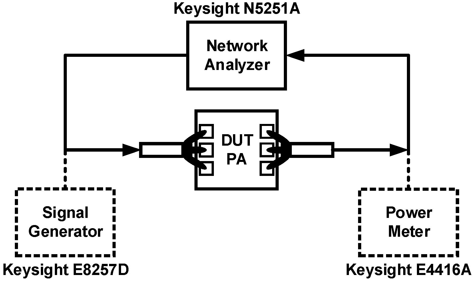
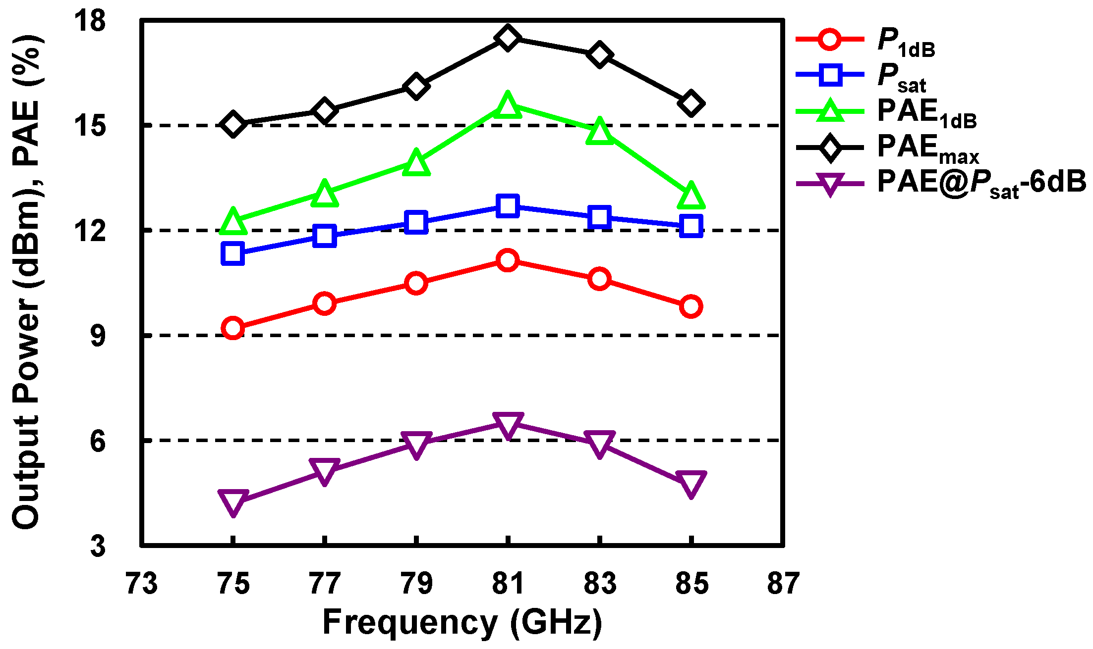
4. Experimental Results

The PA prototype was designed and implemented in a 40 nm CMOS process, and the chip micrograph is shown in Figure 5. The core area of the presented PA is 330 μm × 93 μm, excluding the RF and DC pads. The DC power dissipation is 47 mW at 1 V supply. The supply and bias voltages of the PA are wire-bonded to the printed circuit board (PCB) and the input and output RF pads are accessed using millimeter-wave GSG probes.
The S-parameter and output power measurement setup is shown in Figure 6. The S-parameters are measured from 200 MHz to 110 GHz using a N5251A network analyzer with frequency extenders. The output power is measured using a E8257D signal generator and a E4416A power meter.
The measured S-parameters are shown in Figure 7. The PA achieves a peak small signal gain of 16.8 dB at 70 GHz and a 3 dB bandwidth of about 9 GHz. The S11 is below −10 dB from about 68 to 72 GHz, and S22 is below −13 dB from 71 to 86 GHz. The measured stability factor K is larger than unity, as shown in Figure 8, indicating that the PA is unconditionally stable. Figure 9 shows the simulated S21 at 81 GHz due to the neutralization capacitor variations from the Monte Carlo simulation.
The measured gain, output power, and PAE at 81 GHz are shown in Figure 10. The PA achieved 11.2 dBm P1dB and 12.7 dBm Psat with a P1dB/Psat ratio of 88% in dBm compared to 75% in [2]. The PA exhibited a PAE1dB of 15.6% and a PAEmax of 17.5%. The measured PAE at 6 dB PBO is 6.5%. Figure 11 plots the large-signal performance over 75–85 GHz; the measured P1dB ranges from 9.2 to 11.2 dBm and Psat ranges from 11.3 to 12.7 dBm.
Table 1 summarizes the performance of the E-band PA and compares it with similar works previously published. The PA achieves higher efficiencies at P1dB and 6 dB PBO, as well as a higher P1dB/Psat ratio compared to the previously reported millimeter-wave PAs based on a more advanced CMOS process, indicating that the PA exhibits good linearity. The PA occupies a core area of only 0.031 mm2.

5. Conclusions

A compact E-band PA has been designed and implemented with 40 nm CMOS technology. The output stage of the PA is biased in the deep class-AB region to achieve high efficiencies at P1dB and 6 dB PBO. The circuit design and parameter optimization were carried out with the guidance of impedance formulations. The E-band PA exhibited a P1dB of 11.2 dBm, only 1.5 dB lower than the Psat of 12.7 dBm, with a P1dB/Psat ratio of 88% in dBm compared to the previously reported 75% in [2]. The PA achieved 15.6% PAE1dB, 17.5% PAEmax, and 6.5% PAE at 6 dB PBO with 1 V supply. The comparison with other E-band PAs showed higher efficiencies both at P1dB and 6 dB PBO, with a larger P1dB/Psat ratio.

Author Contributions

Conceptualization, Z.W. and F.H.; methodology, Z.W. and F.H.; validation, Y.Z., X.T. and N.J.; formal analysis, Z.W. and F.H.; investigation, Z.W. and F.H.; writing—original draft preparation, Z.W.; writing—review and editing, F.H.; supervision, F.H.; project administration, F.H. All authors have read and agreed to the published version of the manuscript.

Funding

This research was supported by the National Key Research and Development Program of China under Grant 2019YFB2204701.

Data Availability Statement

Data sharing not applicable.

Conflicts of Interest

The authors declare no conflict of interest.

References

  1. Chen, L.; Zhang, L.; Zhang, L.; Wang, Y. A Compact E-Band PA with 22.37% PAE 14.29 dBm Output Power and 26 dB Power Gain with Efficiency Enhancement at Power Back-off. In Proceedings of the 2019 IEEE Radio Frequency Integrated Circuits Symposium, Boston, MA, USA, 2–4 June 2019; pp. 183–186. [Google Scholar]
  2. Celik, U.; Reynaert, P. An E-Band Compact Power Amplifier for Future Array-Based Backhaul Networks in 22 nm FD-SOI. In Proceedings of the 2019 IEEE Radio Frequency Integrated Circuits Symposium, Boston, MA, USA, 2–4 June 2019; pp. 187–190. [Google Scholar]
  3. Callender, S.; Pellerano, S.; Hull, C. An E-Band Power Amplifier with 26.3% PAE and 24-GHz Bandwidth in 22-nm FinFET CMOS. IEEE J. Solid-State Circuits 2019, 54, 1266–1273. [Google Scholar] [CrossRef]
  4. Callender, S.; Pellerano, S.; Hull, C. A 73GHz PA for 5G Phased Arrays in 14nm FinFET CMOS. In Proceedings of the 2017 IEEE Radio Frequency Integrated Circuits Symposium, Honolulu, HI, USA, 4–6 June 2017; pp. 402–405. [Google Scholar]
  5. Chen, L.; Zhang, L.; Wang, Y.; Yu, Z. A Compact E-Band Power Amplifier with Gain-Boosting and Efficiency Enhancement. IEEE Trans. Microw. Theory Tech. 2020, 68, 4620–4630. [Google Scholar] [CrossRef]
  6. Zhao, J.; Rahimi, E.; Svelto, F.; Mazzanti, A. A SiGe BiCMOS E-Band Power Amplifier with 22% PAE at 18dBm OP1dB and 8.5% at 6 dB Back-Off Leveraging Current Clamping in a Common-Base Stage. In Proceedings of the 2017 IEEE International Solid State Circuits Conference, San Francisco, CA, USA, 5–9 February 2017; pp. 42–43. [Google Scholar]
  7. Ye, W.; Ma, K.; Yeo, K.; Zou, Q. A 65 nm CMOS Power Amplifier with Peak PAE above 18.9% From 57 to 66 GHz Using Synthesized Transformer-Based Matching Network. IEEE Trans. Circuits Syst. I Regul. Pap. 2015, 62, 2533–2543. [Google Scholar] [CrossRef]
  8. Zhao, D.; Reynaert, P. A 60-GHz Dual-Mode Class AB Power Amplifier in 40-nm CMOS. IEEE J. Solid-State Circuits 2013, 48, 2323–2337. [Google Scholar] [CrossRef]
  9. Zhao, D.; Reynaert, P. An E-Band Power Amplifier with Broadband Parallel-Series Power Combiner in 40-nm CMOS. IEEE Trans. Microw. Theory Tech. 2015, 63, 683–690. [Google Scholar] [CrossRef]
  10. Wagner, E.; Rebeiz, G. Single and Power-Combined Linear E-Band Power Amplifiers in 0.12-μm SiGe with 19-dBm Average Power 1-GBaud 64-QAM Modulated Waveforms. IEEE Trans. Microw. Theory Tech. 2019, 67, 1531–1543. [Google Scholar] [CrossRef]
  11. Kaymaksut, E.; Zhao, D.; Reynaert, P. Transformer-Based Doherty Power Amplifiers for mm-Wave Applications in 40-nm CMOS. IEEE Trans. Microw. Theory Tech. 2015, 63, 1186–1192. [Google Scholar] [CrossRef]
  12. Zhao, D.; Kulkarni, S.; Reynaert, P. A 60-GHz Outphasing Transmitter in 40-nm CMOS. IEEE J. Solid-State Circuits 2012, 47, 3172–3183. [Google Scholar] [CrossRef]
  13. Hookari, M.; Roshani, S.; Roshani, S. High-efficiency balanced power amplifier using miniaturized harmonics suppressed coupler. Int. J. RF Microw. Comput.-Aided Eng. 2020, 30, e22252. [Google Scholar] [CrossRef]
  14. Yu, C.; Feng, J.; Zhao, D. A 28-GHz CMOS Broadband Single-Path Power Amplifier with 17.4-dBm P-1dB for 5G Phased-Array. In Proceedings of the 44th European Solid-State Circuits Conference (ESSCIRC), Dresden, Germany, 3–6 September 2018; pp. 38–41. [Google Scholar]
  15. Park, B.; Jin, S.; Jeong, D.; Kim, J.; Cho, Y.; Moon, K.; Kim, B. Highly Linear mm-Wave CMOS Power Amplifier. IEEE Trans. Microw. Theory Tech. 2016, 64, 4535–4544. [Google Scholar] [CrossRef]
  16. Nocera, C.; Papotto, G.; Cavarra, A.; Ragonese, E.; Palmisano, G. A 13.5-dBm 1-V Power Amplifier for W-Band Automotive Radar Applications in 28-nm FD-SOI CMOS Technology. IEEE Trans. Microw. Theory Tech. 2021, 69, 1654–1660. [Google Scholar] [CrossRef]
  17. Mosalam, H.; Xiao, W.; Pan, Q. A 50-82 GHz broadband cascode-based power amplifier in 40 nm CMOS. Int. J. Electron. Commun. 2021, 137, 153824. [Google Scholar] [CrossRef]
  18. Xi, T.; Huang, S.; Guo, S.; Gui, P.; Huang, D.; Chakraborty, S. High-Efficiency E-Band Power Amplifiers and Transmitter Using Gate Capacitance Linearization in a 65-nm CMOS Process. IEEE Trans. Circuits Syst. II Express Briefs 2017, 64, 234–238. [Google Scholar] [CrossRef]
  19. Khalaf, K.; Vidojkovic, V.; Long, J.; Wambacq, P. A 6x-Oversampling 10GS/s 60GHz Polar Transmitter with 15.3% Average PA Efficiency in 40nm CMOS. In Proceedings of the 44th European Solid-State Circuits Conference (ESSCIRC), Graz, Austria, 14–18 September 2015; pp. 348–351. [Google Scholar]
Figure 1. Schematic of the presented E-band PA.
Electronics 11 01679 g001
Figure 2. Simulated P1dB, Psat, and gain versus the transistor current density at 81 GHz at 1 V supply: (a) output stage; (b) driver stage.
Electronics 11 01679 g002
Figure 3. TMN circuit model for (a) output matching, (b) inter-stage matching.
Electronics 11 01679 g003
Figure 4. Calculated ko and no according to Equations (2) and (3) for Lo2 ranging from 30 to 400 pH.
Electronics 11 01679 g004
Figure 5. Chip micrograph of the PA.
Electronics 11 01679 g005
Figure 6. The measurement setup for S-parameters and output power.
Electronics 11 01679 g006
Figure 7. Measured S-parameters versus frequency.
Electronics 11 01679 g007
Figure 8. Measured stability factor K versus frequency.
Electronics 11 01679 g008
Figure 9. The simulated S21 at 81 GHz due to neutralization capacitor variations from the Monte Carlo simulation with 500 random runs.
Electronics 11 01679 g009
Figure 10. Measurement results of gain, output power, and PAE at 81 GHz.
Electronics 11 01679 g010
Figure 11. Measurement results of P1dB, Psat, PAE1dB, PAEmax and PAE@Psat-6 dB over 75–85 GHz.
Electronics 11 01679 g011
Table 1. E-band PA performance comparison.
Ref. YearTech.Freq.
(GHz)
Supply
Voltage (V)
Num. of StagesGain
(dB)
P1dB
(dBm)
Psat
(dBm)
PAE1dB
(%)
PAEmax
(%)
PAE@Psat-
6 dB (%)
Core Area (mm2)
[2], 201922 nm FD-SOI762217.813.317.88.1 *17.34.3 *0.02
[3], 201922 nm Fin-FET751216.65.712.811.626.3-0.054
[5], 202065 nm CMOS731.2326–3112.014.313.322.45.60.025
[16], 202128 nm FD-SOI771326.510.013.58.0 *14.5-0.15
[17], 202140 nm CMOS702210.910.814.011.015.04.0 *0.075
[18], 201765 nm CMOS751.3321.414.617.311.2 *18.95.00.09
[19], 201528 nm CMOS600.9324.37.410.8-22.4 **5.3 *0.18
This work40 nm CMOS811212.511.212.715.617.56.50.031
* Estimated from reported figures; ** drain efficiency.
Publisher’s Note: MDPI stays neutral with regard to jurisdictional claims in published maps and institutional affiliations.

