Article

Compact CMOS Wideband Instrumentation Amplifiers for Multi-Frequency Bioimpedance Measurement: A Design Procedure

by
Israel Corbacho
,
Juan M. Carrillo
*,
José L. Ausín
,
Miguel Á. Domínguez
,
Raquel Pérez-Aloe
and
Juan Francisco Duque-Carrillo
Departamento de Ingeniería Eléctrica, Electrónica y Automática, Universidad de Extremadura, Avenida de Elvas s/n, 06006 Badajoz, Spain
*
Author to whom correspondence should be addressed.
Electronics 2022, 11(11), 1668; https://doi.org/10.3390/electronics11111668
Submission received: 5 May 2022 / Revised: 20 May 2022 / Accepted: 21 May 2022 / Published: 24 May 2022
(This article belongs to the Section Microelectronics)

Abstract

:
The design of an instrumentation amplifier (IA), based on indirect current feedback and suited to electrical bioimpedance spectroscopy, is presented. The IA consists of two transconductors and a summing stage, featuring a single-stage configuration process that allows the maximum achievable bandwidth to be extended. The transconductors are linearized by means of resistive source degeneration, whereas the use of super source followers allows a reduction in the values of the source degeneration resistors. This fact leads to a decrease in the overall noise and the silicon area, thus resulting in a compact implementation. A thorough analysis of the proposed solution, accompanied by a design procedure and verified by means of electrical simulations, is also provided. Two versions of the IA, i.e., a single-ended (SE) and a pseudo-differential (PD) structure, were designed and fabricated using 180 nm CMOS technology to operate with a 1.8 V supply. The experimental results, including a BW of 5.2 MHz/8.0 MHz, a CMRR higher than 72 dB/80 dB, a DC current consumption of 139.0 μ A/219.3 μ A and a silicon area equal to 0.0173 mm 2 /0.0291 mm 2 for the SE/PD implementation, validate the suitability of the approach.

1. Introduction

Electrical bioimpedance measurements allow for the characterization of biological media according to their electrical properties [1]. To this end, the biological impedance under study ( Z U T ) is electrically excited by a sinusoidal signal, whereas the internal composition is determined in terms of the magnitude and phase angle of the corresponding response. The measurement of bioimpedance at a given single frequency is known as bioelectrical impedance analysis, whereas bioelectrical impedance spectroscopy refers to the determination of the impedance in a certain frequency range. Furthermore, the characterization of temporary alterations in the Z U T and the detection of transient physiological events require the use of a multi-frequency bioimpedance analysis.
The conceptual scheme of a typical bioimpedance measurement system is illustrated in Figure 1, in single-output and differential-output versions. A sinusoidal voltage or current can be indistinctly used as an excitation signal, and it ismuch more common to base the bioimpedance analysis on an injected current signal, I e x c , to avoid any damage in the biological Z U T . The amplitude of the excitation current signal is chosen with such a low intensity, in the range of the μ As and always lower than 1 mA, that the bioimpedance technique, in addition to being non-invasive, economic, slight, and easy-to-use, results in innocuous effects. The typical frequencies of electrical signals used in bioimpedance technology range from several hundreds of Hz to a few MHz, which is known as the β -dispersion range. The phase angle, and therefore the reactive component of the bioimpedance in this frequency band, provides valuable information, for instance, on the state of the plasma membrane (cell membrane), which is in turn a good indicator of cellular health.
Once the Z U T is properly excited, the corresponding voltage drop that is generated can be measured by means of an instrumentation amplifier (IA) [2,3,4,5,6,7,8,9,10,11,12,13,14,15,16,17,18,19,20,21,22,23,24,25,26,27,28,29,30,31,32,33,34,35,36,37,38,39,40,41,42], whereas signal conditioning [41,43] may be subsequently required prior to signal processing. Taking into account the characteristics of the measurement procedure described above, the features of the IA can be determined. On the one hand, the levels of the signals to be processed can be maintained within a certain range through the appropriate programming of the value of the excitation current. In this way, the voltage signal across the impedance under study will be in the mV range and, consequently, low amplification levels and a linear response over a determined input voltage range are required. On the other hand, a relatively wide bandwidth (BW) is mandatory, in order to properly operate over the entire frequency range considered in the bioelectrical impedance measurement application. It is worth pointing out that the IA, beyond providing a certain signal amplification, allows the buffering of the sample under study, as well as the adaptation of the DC levels of the signals at the Z U T and at the input of the signal conditioning system. Furthermore, excessive amplification would impose a constraint on subsequent stages, as their operating voltage ranges would be correspondingly increased.
Current feedback (CF) is a suitable technique used to implement an integrated IA [2,5,6,7,10,15,18,22,26,33,35]. Indeed, this solution uses an input transconductor to process the input signal and an output (or feedback) transconductor to feed the output signal back in current form. By following this approach, the amplification factor of differential-mode (DM) signals can be set in a straightforward manner, whereas circuit stability can be easily ensured over a wide frequency range. Moreover, the solution leads to a circuit structure that is more compact and which has much lower power consumption as compared to the traditional three-op ampstructure [3,9]. Additionally, it is worth mentioning that the rejection of common-mode (CM) signals, evaluated by means of the CM rejection ratio (CMRR), is carried out at the input stage and can be enhanced by means of appropriate balancing and isolation techniques. Different approaches to implementing the CF in an IA have been proposed. The first IAs based on CF included a feedback loop around the input and/or the output transconductor in order to equalize the biasing currents as a function of the input signal level [2], which was later popularly known as local current feedback (LCF) [15,18,26]. In addition, direct current feedback (DCF) [4,5] was proposed to include the input and output transconductors in the same branches of the circuit implementation, in order to simultaneously reduce the power consumption and achieve higher compactness. Nevertheless, this configuration is not appropriate for operation under low supply voltages, due to the multiple stacking of devices. Alternatively, indirect current feedback (ICF) [6,33,35] was proposed for low-voltage operation, maintaining a similar operation principle as that of DCF.
An appealing characteristic of an ICF IA is that the input CM voltage range can be suited to the intended application, either by using an input voltage level shifter or by directly adjusting the aspect ratios of certain transistors. Indeed, in a single-output configuration, such as the one illustrated in Figure 1a, the Z U T is usually connected to a voltage level close to ground. This imposes on the IA the capability to operate around this voltage region. On the other hand, if one is aiming at a differential structure, as is the case depicted in Figure 1b, a balanced excitation circuit must be used, which locates the input CM voltage range of the signal to be acquired by the IA around the midsupply. In both cases, the input CM voltage range of the IA must be adapted to the DC level of the signal.
In this contribution, the design of an IA based on the ICF technique that leads to a wide BW and is able to process relatively large input signals with a reduced power consumption is described. Two different realizations, namely, a single-ended (SE) and a pseudo-differential (PD) structure, are presented. Both of them have been implemented in 180 nm CMOS technology to operate with a supply voltage of 1.8 V. The experimental characterization of the silicon prototypes shows the suitability of the proposal to be used in a bioimpedance measurement system. The rest of the manuscript has been organized as follows. Section 2 deals with the structure of the ICF IA, considering both the block diagram and the transistor level implementation. A design procedure, which includes a theoretical analysis and the corresponding simulated design space, is proposed in Section 3. The experimental characterization of the two IAs is reported in Section 4 and conclusions are drawn in Section 5.

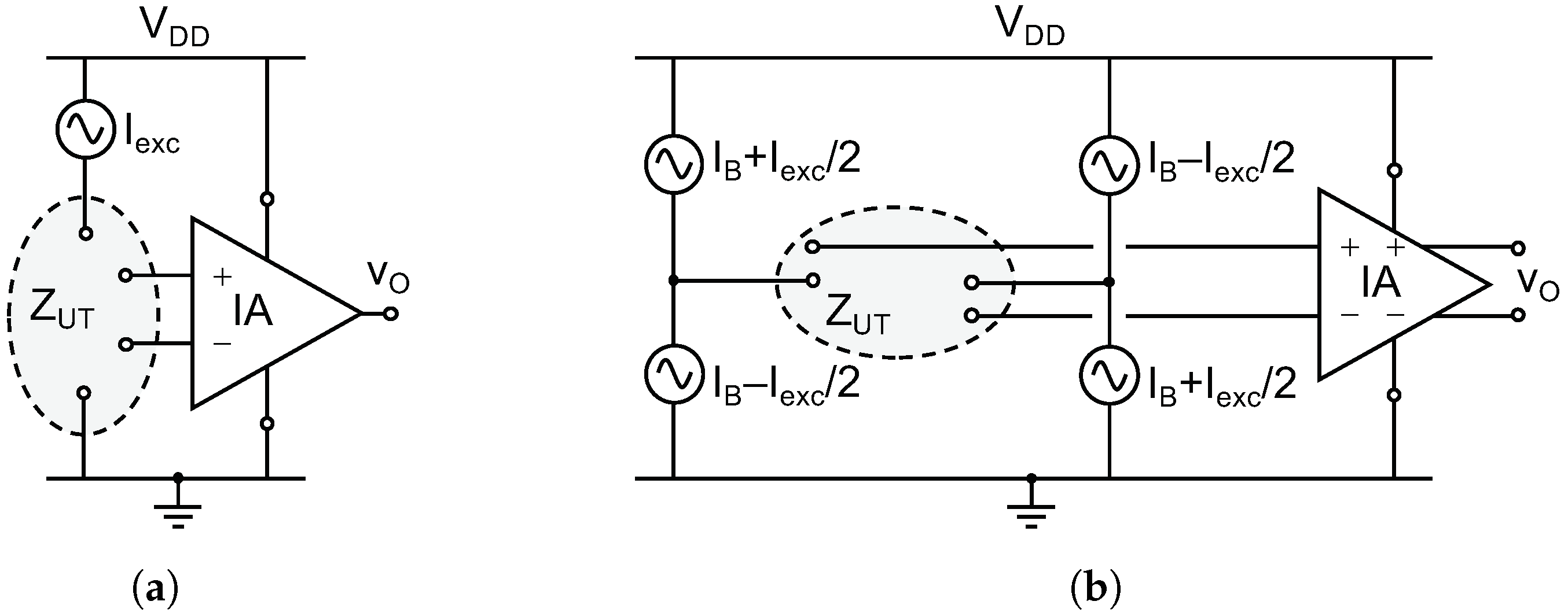
2. Principle of Operation
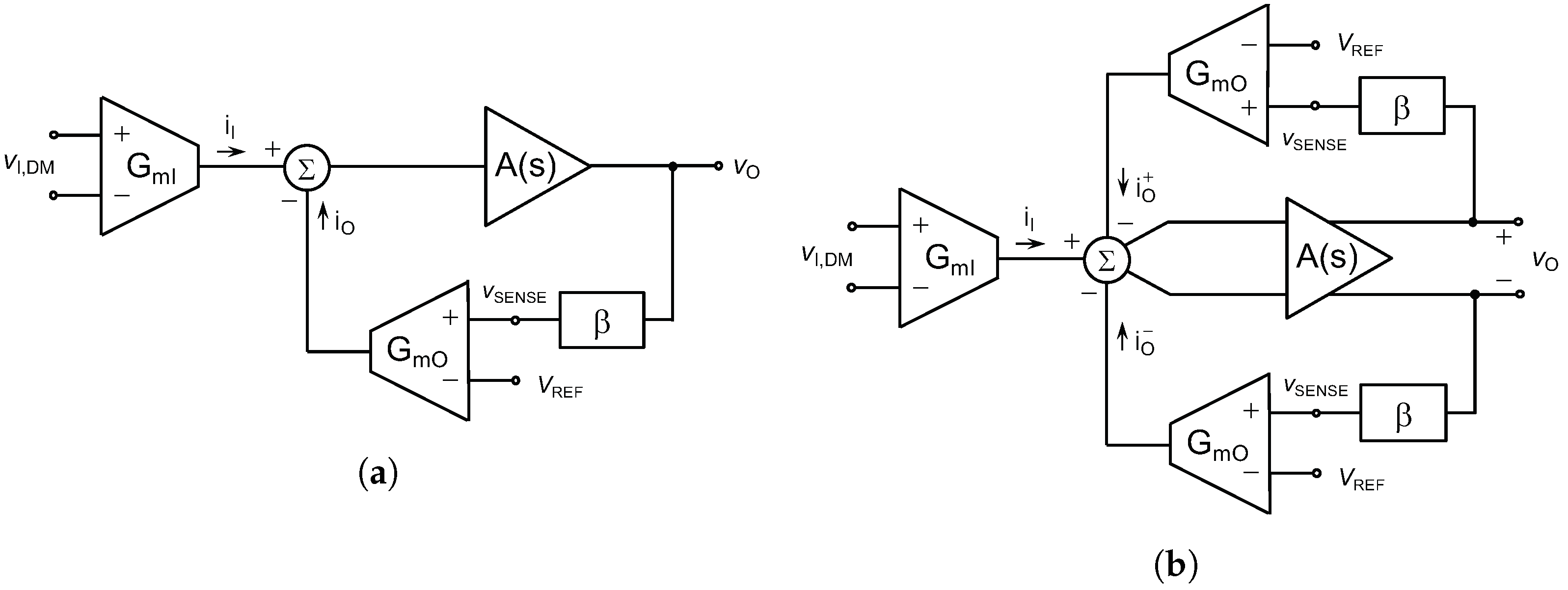
2.1. Block Diagram

A conceptual block diagram of an ICF IA is illustrated in Figure 2a, where G m I and G m O are the input and the output (or feedback) transconductors, respectively; Σ is a summing stage in which the output currents of G m I and G m O are added; A ( s ) is an inverting gain stage; and β is the feedback network. The voltage-to-current (V-to-I) converter G m I generates current i I from the input voltage, v I , D M , whereas an output current i O is produced by the transconductor G m O when a voltage v S E N S E V R E F is applied to their input terminals. The voltage v S E N S E is a scaled replica of the output voltage, v O , and V R E F is a reference voltage used to set the DC component of v O to the intended level. The A ( s ) stage can be omitted, i.e., A ( s ) = 1 , in order to obtain a single-stage IA, or may be implemented by means of a first-order section, so that the gain of the feedback loop can be further increased.
The transfer function of the system illustrated in Figure 2a can be expressed as:
H ( s ) v o ( s ) v i ( s ) = G m I · R o u t 1 s C o u t · A ( s ) 1 + β · G m O R o u t 1 s C o u t · A ( s )
where R o u t and C o u t are the output resistance and capacitance, respectively, of the summing stage. Provided that the loop gain around transconductor G m O is sufficiently high, the voltage gain, A v , and the BW of the IA can easily be deduced from (1) to be
A v v o v i , d m = 1 β · G m I G m O
B W = β · G m O C B W
where C B W is the capacitor used to make the feedback loop stable, i.e., a load capacitor, C L , or a compensation capacitor, C C , depending on whether the IA consists of one or two gain stages, respectively. The gain of the IA can be adjusted by means of the ratio of the input and output transconductances, with the latter also compromisedin the setting of the bandwidth.
In cases in which the bioimpedance measurement system follows the scheme illustrated in Figure 1b, the block diagram in Figure 2a can be easily translated into a differential structure, as depicted in Figure 2b. Even though two output transconductors are required in this case, the need for a specific block to control the CM output voltage is avoided, as detailed in Section 2.2.

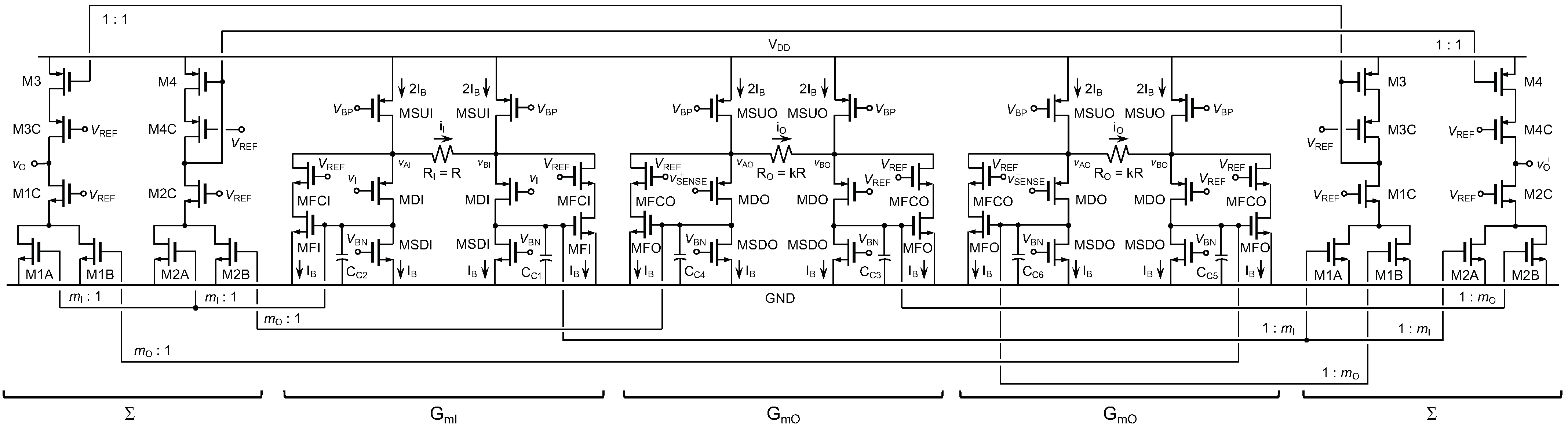
2.2. Transistor Level Implementation

The transistor level implementation of a SE ICF IA, following a single-stage approach, i.e., A ( s ) = 1 , and connected in a unity gain feedback configuration, that is, β = 1 and v O = v S E N S E , is detailed in Figure 3. The principle of operation of the input and output transconductors is based on converting a voltage into a current on a resistor. Two voltage followers are used to isolate the input and output resistors, R I and R O , respectively, from preceding and subsequent stages. To this end, the block known as a super source follower (SSF) is used [33,35]. Indeed, the implicit feedback in an SSF, established by transistor MFI(O) around the signal driver transistor MDI(O), leads to lower output resistance of the buffer. This fact greatly reduces the impact of the source degeneration resistor on the gain of the voltage follower and allows one to decrease the value of R I ( O ) . The effective transconductance generated by the input and output V-to-I cells is equal to:
G m , e f f i I ( O ) v D M = 2 R I ( O ) 1 1 + 1 + 2 R I ( O ) 1 g m , M D I ( O ) g o , M D I ( O ) + g o , M S D I ( O ) g m F I ( O ) 2 R I ( O )
where g m , M i I ( O ) and g o , M i I ( O ) are the transconductance and output conductance, respectively, of transistor Mi at the input (I) or output (O) transconductor; R I ( O ) is the source degeneration resistor ( R I or R O ); and g m g o has been assumed. The first term in (4), which is inversely proportional to R I ( O ) , represents the ideal transconductance of the V-to-I converter if the voltage followers were completely ideal, whereas the second contribution accounts for the loading effect of the source degeneration resistor on the voltage followers. As inferred from (4), the feedback loop implicit in the SSF greatly reduces the second-order dependence of the trasnconductance on R I ( O ) , and the last term can be approximated to unity [35].
The input CM voltage range of the proposed IA can be flexibly adjusted. Indeed, the operation for input signals around the midsupply is intrinsically granted merely by setting the aspect ratio of the input devices correctly so that the MSUI transistors, working as current sources, can operate in saturation, i.e., V S D , M S U I | V D S a t , M S U I | . Moreover, the operation for input signals around ground, as in the case illustrated in Figure 1a, can be easily achieved through the proper sizing of the MFI transistors. Indeed, the voltage at the drain of MDI transistors, which could force their operation in the triode region, can be reduced to an appropriate level by increasing the aspect ratio of MFI transistors, thus ensuring the operation of the input drivers in saturation.
The current signals generated by G m I and G m O are conveyed to the output node of the IA by means of current mirrors with gains of 1 : m I and 1 : m O , respectively. Furthermore, the transconductances obtained in the input and output V-to-I converters are inversely proportional to R I and R O , which are referred to here as R I = R and R O = k · R for convenience. The current gains m I and m O and resistor ratio k = R O / R I form a set of design parameters that provides the circuit with additional design flexibility in order to adjust the voltage gain and bandwidth of the IA to the intended values. Indeed, in view of the circuit implementation method proposed in Figure 3, the general transfer function in (1) for the ICF IA can be rewritten as:
H ( s ) = m I G m I m O G m O 1 + s C L m O G m O
where C L is the load capacitor connected to the output of the IA. Cascode MFCI(O) transistors, shown in Figure 3, allow the enhancement of the accuracy of the current mirrors with gains of m I and m O . In addition, capacitors C C 1 to C C 4 are used to optimize the phase margin of the feedback loop inherent in each SSF cell.
The differential implementation of the proposed ICF IA is shown in Figure 4. As observed, there are two output V-to-I converters, each of which is used to compare one of the two output voltages, v O + and v O , with the reference voltage V R E F . Unlike in the case of a fully-differential structure, no CM feedback (CMFB) circuit is required to control the CM component of the output voltage, as two feedback loops around the two output transconductors are established, thus stabilizing each output node individually. Therefore, the proposed differential structure can be classified as pseudo-differential. In any case, the differential structure of the input transconductor carries out the rejection of input CM signals, thus ensuring a high CMRR. As the PD ICF IA is intended to operate in the configuration illustrated in Figure 1b, operation for input CM signals around the midsupply can be ensured by using an aspect ratio for MFI transistors that are much smaller as compared to the SE approach.

3. Design Guidelines

The main features of an ICF IA are analyzed here in order to determine the potential design space as a function of the design options available, in particular, of the parameters set [ m I , m O ,k]. The expressions obtained are validated by means of simulations and a design procedure is proposed.

3.1. Theoretical Analysis
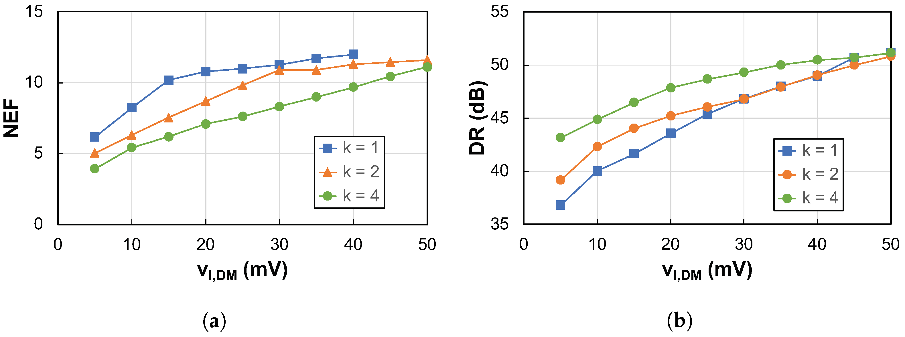
Gain and bandwidth: Taking into account the transfer function of a single-stage ICF IA, given in (5), along with the expression of the effective transconductance in (4), the following expressions for the A v and the BW are obtained:
A v = m I G m I m O G m O = k m I m O · 1 + 1 + 2 k R 1 g m , M D O g o , M D O + g o , M S D O g m , M F O 1 + 1 + 2 R 1 g m , M D I g o , M D I + g o , M S D I g m , M F I k m I m O
B W = G m O C L = m O k · 2 C L R · 1 1 + 1 + 2 k R 1 g m , M D O g o , M D O + g o , M S D O g m , M F O m O k · 2 C L R
From these equations, interesting design guidelines may be inferred. First, the voltage gain of the IA in (6) is in the first order of approximation, according to the dominant term, proportional to k and m I and inversely proportional to m O . Secondly, the load regulation effect in the input and output V-to-I converters may be cancelled by making k = 1 , that is, R I = R O . Otherwise, A v deviates from the value given by the dominant term and the error increases as k is made larger. Finally, the BW in (7) is proportional to m O and inversely proportional to k. Thus, a modification of the value of k may be counteracted by a change of m O in the same sense without affecting the speed and stability conditions of the feedback loop. It is worth pointing out that if the voltage gain of the IA is set by means of parameter k, the saturation of transconductors G m I and G m O rises simultaneously, as v O is k times larger than v I , but R O is also k times bigger than R I . Nevertheless, if A v is increased by raising the value of m I with respect to m O , whereas k is fixed equal to unity, the amplification of the output signal will force G m O to saturate before G m I .
CMRR: Ideally, only a fully-balanced DM signal can produce an output current in a transconductor. Nevertheless, in the presence of mismatches, CM signals can also lead to an output current in a real V-to-I converter. We can define the residual transconductance as follows:
Δ G m i v C M
where v C M is the CM signal applied to the input of the transconductor. The small-signal equivalent model of the V-to-I converters used in the proposed ICF IA has been analyzed to determine the residual transconductance due to the presence of a CM input signal. To this end, for each pair of matched devices in the implementation, the small-signal parameter g i has been supposed to be g i + Δ g i / 2 and g i Δ g i / 2 , respectively. The main contributions to Δ G m , after having analyzed and quantified all of them, were found to be due to MD transistors, i.e., Δ g m , M D and Δ g o , M D , and may be expressed as follows:
Δ G m | Δ g m , M D 2 R · Δ g m , M D g o , M D g m , M D 2 · 1 1 + 2 R 1 g m , M D g o , M D + g o , M S D g m , M F
Δ G m | Δ g o , M D 2 R · Δ g o , M D g m , M F · 1 1 + 2 R 1 g m , M D g o , M D + g o , M S D g m , M F
The impact of the transconductance and output conductance mismatches of other transistors on Δ G m is negligible and, hence, is not reported for the sake of conciseness. The contribution of the residual transcoductance can be disregarded in the output transconductor of the ICF IA, as it is much lower as compared to the effective transconductance. Nevertheless, this parameter plays a key role at the input V-to-I converter, since it gives an idea of the rejection to CM signals. In this respect, it is worth pointing out that the feedback loop inherent in an SSF also helps to reduce the load regulation effect of resistor R on the voltage followers, as may be inferred from the rightmost terms in (9a) and (9b).
The CMRR, defined as the ratio of the DM and CM gains of the IA, can be written as
C M R R A v A c m = m I G m I m O G m O m I Δ G m I m O G m O = G m I Δ G m I = 1 Δ g m , M D I g o , M D I g m , M D I 2 + Δ g o , M D I g m , M F I · 1 + 2 R I 1 g m , M D I g o , M D I + g o , M S D I g m , M F I 1 + 1 + 2 R I 1 g m , M D I g o , M D I + g o , M S D I g m , M F I
The last fraction in the rightmost term of the previous equation represents the quotient between the load regulation effects of resistor R for the CM and the DM signals, respectively. The use of SSF cells allows it to approach unity if the value of the source degeneration resistor in the input transconductor is not excessively low, i.e., higher than 1 k Ω for practical purposes. Similar theoretical analyses can be carried out for the offset voltage and the power supply rejection ratio (PSRR), which are also influenced by device mismatches. Regarding the offset voltage, the response of the CMRR gives an idea of its behavior, as they are inversely proportional. As for the PSRR, most bioimpedance measurement applications are battery-operated and hence this is not a critical metric in our case.
Noise: Noise is another key metric to be considered in an IA. In those cases where the input signals are restricted to the low frequency range, different techniques for noise reduction, especially of the flicker component, have been considered [11,12,16,19,20,21,23,25,31,32]. Nevertheless, in bioimpedance spectroscopy, the frequency range that is typically considered is sufficiently wide to assume that thermal noise is dominant. In the ICF IA in Figure 3, the main contributions to the input’s referred noiseare due to the devices in the input transconductor. In particular, the IA noise power spectral density can be approached as follows:
v i N , t h 2 Δ f = 1 + 1 + 2 R I 1 g m , M D I g o , M D I + g o , M S D I g m , M F I 2 4 k T R I 1 + 4 3 g m , M D I + g m , M S U I R I
where k is Boltzmann’s constant and T is the absolute temperature. The first term in (11), which is the inverse of the load regulation effect of resistor R I on the SSF sections, is the conversion factor for referring noise to the input; the second term is the thermal noise of resistor R I ; and the last term accounts for the noise contributions of the devices involved in the circuit implementation of the input V-to-I converter, G m I . It becomes apparent from (11) that the noise of the IA can be reduced by decreasing the value of the source degeneration resistor R I , which is possible thanks to the use of improved voltage followers, that is, of SSF cells.
Figures of merit: Some of the metrics considered in our analysis are included in a well-known parameter used to compare different IAs, the noise efficiency factor (NEF). This figure of merit (FoM) describes how many times the noise of a system is higher as compared to the white noise of an MOS transistor with the same drain current and bandwidth [5] and is defined as:
N E F = V i N , r m s 2 I D D π V T 4 k T B W
where I D D and V T are the total DC current flowing through the IA and the thermal voltage, respectively. This is a fair parameter for comparison when the amplitude of the signals to be processed is kept to a low extent. Nevertheless, when large input signals must be processed a high biasing current is required, which leads to a penalty in therms of NEF. Thus, an FoM that takes the signal amplitude into account, such as the dynamic range (DR), can be used in a complementary way. The DR is defined as:
D R = 20 · log v I , D M m a x V i N , r m s
Moreover, in the particular implementations of the IA illustrated in Figure 3 and Figure 4, the maximum input signal is given by
v I , D M m a x = A v , S S F · R · I B
where A v , S S F is the voltage gain of the SSF cells, which for practical purposes can be supposed to be equal to unity. Indeed, the condition for one of the MFI feedback transistors entering the cut-off region is that a maximum current equal to I B flows through the source degeneration resistor. Different approaches to objectively determining the value of v I , D M m a x can be established, with a widespread criterion involving the consideration of the amplitude of the input signal that leads to 1% of total harmonic distortion (THD).

3.2. Design Space

Based on the above analysis, it is clear that a same value of the voltage gain, A v , can be obtained with different combinations of the design parameters m I , m O , and k. The most straightforward and common solution is to set the gain of the IA through the ratio k of the output and input degenerations resistors, R O and R I , respectively [15,35]. Nevertheless, as is evident from (6), this choice causes the theoretical value of A v to deviate from the expected nominal value, with this deviation increasing for increasing values of k. Conversely, k can be made equal to unity and the gain of the IA can be set by means of the ratio m I / m O . In such a case, special care is required as the BW of the IA relies directly on m O , and in particular, is directly proportional to the term m O / k .
In order to determine the design space available for an ICF IA, in terms of A v , BW, CMRR, and noise, and as a function on the combination of the design parameters [ m I , m O ,k], a case of study has been carried out. First, a nominal voltage gain A v , n o m = 4 V/V has been selected, the value of which is in agreement with the relatively low values of the voltage gain required in bioimpedance measurement systems. Then, all the combinations of m I , m O , and k leading to the desired value of A v have been determined, leading to the choices summarized in Table 1. Finally, the metrics A v , BW, CMRR, and the input referred thermal noise haven been analytically calculated from their corresponding expressions in (6), (7), (10), and (11) when the resistor R is varied in the range [200 Ω −20 k Ω ]. The theoretical results have been compared to simulations of the IA in Figure 3, designed using CMOS 180 nm technology to operate with a supply voltage equal to 1.8 V.
In Figure 5a the voltage gain A v of the IA is represented, including both the results predicted by the analysis and the simulated response. For the case of k = 1 both types of results, theoretical and simulated, were extremely close to the nominal value of the voltage gain, i.e., 4 V/V, even for very low values of R. Indeed, the error of the theoretical response was exactly equal to zero, whereas the maximum error of the simulated behavior, not appreciable in Figure 5a, was only 0.1%. ln the other two cases, k = 2 and k = 4 , there was a noticeable dependence of A v on R, with the most optimal results occurring around R = 5 k Ω . The higher the value of k, the larger the difference between the load regulation effects due to R I and R O and, hence, as predicted by (6), the larger the error in A v with respect to the expected value A v , n o m .
The behavior of the BW of the IA is illustrated in Figure 5b, where again the analytical and simulated responses are represented against the value of resistor R. In both cases the value of the load capacitor, C L , was set to 180 pF, a relatively high value that allows the splitting of the position of the dominant and the secondary pole of the feedback loop established around the output transconductor of the IA. As observed, the BW increases as the value of the source degeneration resistor R is reduced, which is consistent with (7). Thus, it can be concluded that the simulated value of the BW can be predicted by (7) with fairly high accuracym provided that the feedback loop around G m O displays a response similar to a one-pole system. Otherwise, the impact of secondary poles on the BW should be taken into account in the analytical expression.
The CMRR at DC was also considered in our case study. On the one hand, it was theoretically estimated according to the G m / Δ G m ratio, as indicated in (10), selecting a mismatch for g m , M D I and g o , M D I equal to 0.1%. Moreover, the CMRR, defined as the quotient of the differential-to-differential gain over the common-to-differential gain, was obtained through a 500-run Montecarlo analysis, including mismatches and process variations. A comparison of the results obtained is illustrated in Figure 5c. It may be observed that the data calculated were the same for k values equal to 1, 2 and 4, as the value of k is not present in (10). Indeed, the CMRR essentially relies on the response of the input transconductor and, hence, the value of k has no impact on its value. It may be observed in Figure 5c that a reasonably good agreement was demonstrated between the theoretical and simulated values of the CMRR, even though the values of the mismatches assumed for the devices involved in (10) were found to be critical.
In view of the frequency range considered in our application, white noise would be dominant over flicker, or 1/f, noise. For this reason, only thermal noise was taken into account in the theoretical analysis and, consequently, considered in (11). In Figure 5d the theoretical value of the input referred noise power spectral density is represented as a function of R, along with the simulated values of the same metric. In both cases, only the white noise component has been taken into account. As observed, the expression in (11) gives a rough idea of the thermal noise behavior, with noticeable differences arising due to the contributions of other devices that were not included, for the sake of simplicity, in the theoretical calculation of the noise. Therefore, there is an evident trade-off between the complexity of (11) and its accuracy.
Considering the design space created for the proposed ICF IA, illustrative conclusions can be drawn. First, the influence of the parameter k on the voltage gain can be partially counteracted by selecting a value that is not excessively low for R. Moreover, low values of the source degeneration resistor lead to a lower noise figure, thus imposing a design trade-off in the selection of the value of R. Finally, it is worth mentioning that the lower bound for the value of R is determined through the achievement of an appropriate phase margin for the feedback loop established around G m O , which can be adjusted by properly selecting the value of the load capacitor. Indeed, the loading of the IA using only parasitic capacitances may not be sufficient to make the IA stable, and this can be easily overcome by connecting an on-chip load capacitor at the output terminal.

3.3. Design Procedure

To illustrate the analytical and simulated response of the IA described in the previous subsection, a very high value of the load capacitor C L was assumed, whereas the value of the source degeneration resistor R was swept.Indeed, a high value of C L allows for the overcompensation of the frequency response of the IA so that the dominant and the secondary poles are sufficiently far away from each other even for very low values of R, that is, for high values of the BW. Nevertheless, this approach is only useful for inspecting the possible design options, as an optimal methodology in the design of the ICF IA. In this respect, the following design procedure is proposed:
  • Determine the combinations of the design parameters [ m I , m O , k ] that lead to the desired value of A v and provide the same BW.
  • Select an option for [ m I , m O , k ] and set the value of the source degeneration resistor R in view of the responses of A v , BW, CMRR and the noise.
  • Fix the value of the input DM signal range, v I , D M m a x .
  • Find the value of the biasing current I B that leads to v I , D M m a x according to (14). This value can be refined by means of simulations establishing an objective criterion, such as obtaining 1% of THD when v I , D M m a x is applied.
  • Determine the value of C L that leads to a phase margin of 60º for the feedback loop around G m O .
  • Calculate the NEF and the DR based on (12) and (13), respectively.
A summary of the simulated behavior of the ICF IA, in terms of the NEF and the DR as a function of v I , D M , is depicted in Figure 6, considering the combinations for [ m I , m O ,k] indicated in Table 1. A source degeneration resistor R = 5 k Ω was chosen, representing a good design trade-off between selecting a moderately high value and avoiding an excessive loading effect on the SSF sections. Furthermore, values of I B and C L in the ranges [0.7, 7.8] μ A and [14.3, 1.3] pF were selected for each value of v I , D M varying between 5 mV and 50 mV of amplitude. The maximum value of the input DM voltage was limited by the requirement of having a THD below 1%. As a result, the BW and the input referred noise integrated from 1 Hz to the BW frequency were in the ranges of [0.7, 12.3] MHz and [24.6,98.1] μ V r m s , respectively. The NEF, shown in Figure 6a, is minimized for the case k = 4, whereas the DR, represented in Figure 6b, displays the highest values for this same value of k. It may be observed in Figure 6a that for k = 1 the NEF is not shown for v I , D M values larger than 40 mV. Indeed, as indicated previously, an excessive level of the input voltage leads to the saturation of the output transconductor, G m O , causing a corresponding drop in the BW and a huge increase in the NEF. In view of the results in Figure 6, it can be concluded that setting the voltage gain of the IA by means of the ratio k = R O / R I leads to the lowest NEF and the highest DR, allowing the operating voltage range to be maximized.

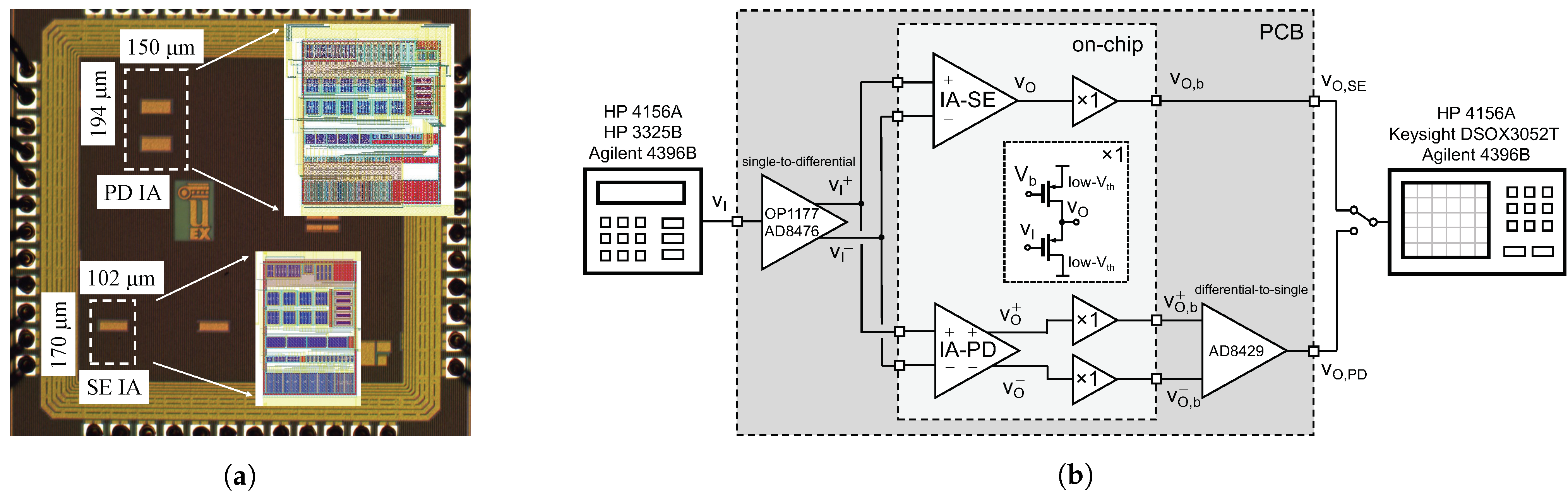
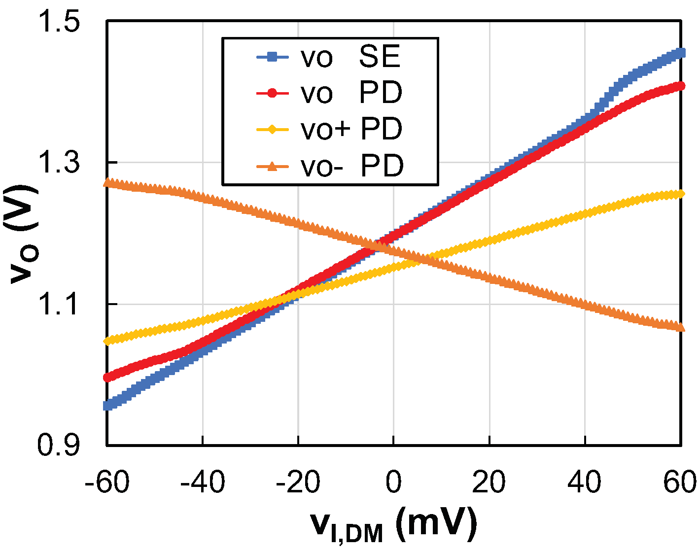
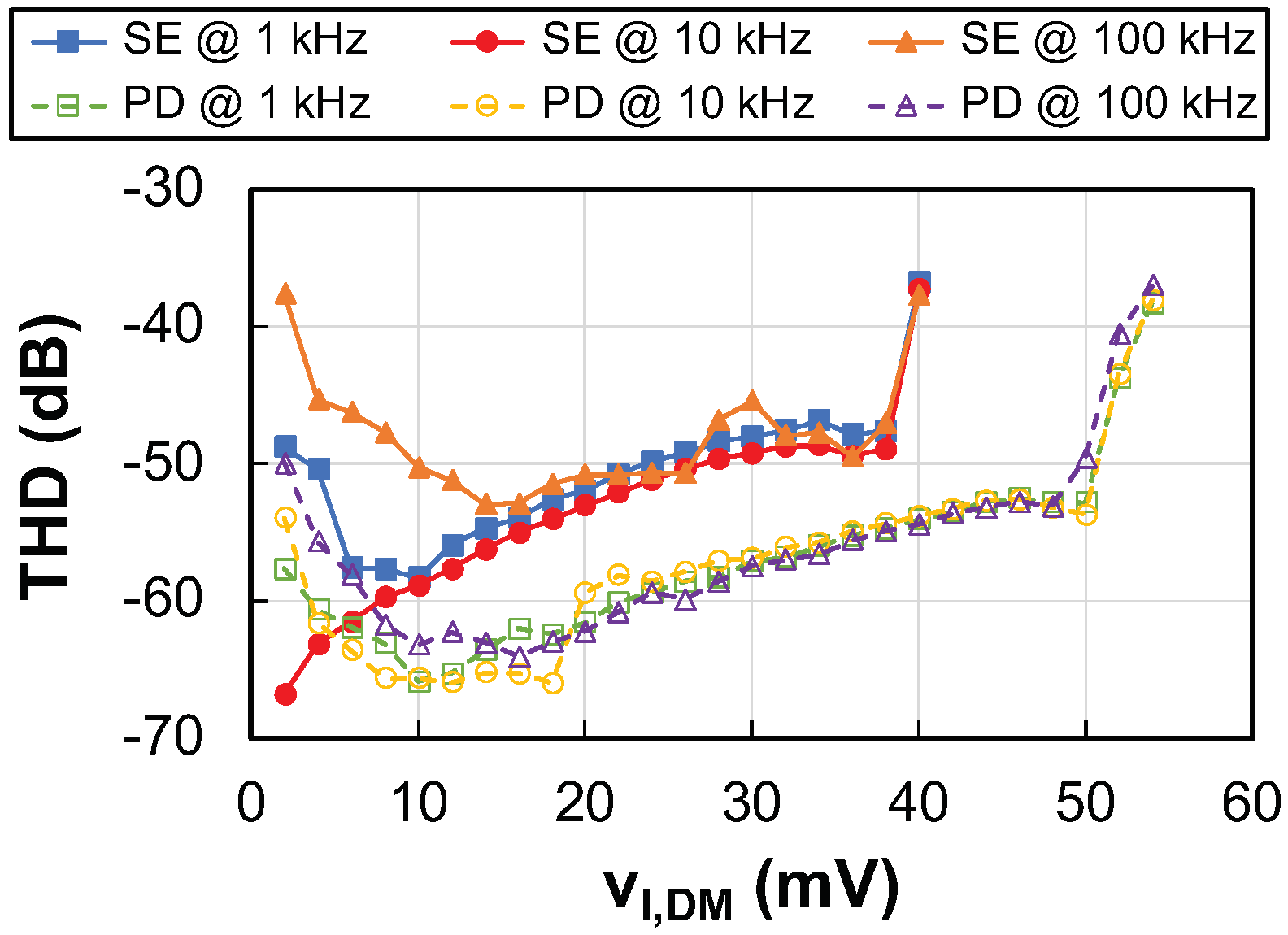
4. Experimental Results

The single-ended and pseudo-differential versions of an ICF IA including SSF cells, illustrated in Figure 3 and Figure 4, respectively, were designed using UMC 180 nm CMOS technology to operate with a supply voltage of 1.8 V. Simulations were carried out with the Cadence® Tools Suite, Spectre simulator, and the BSIM3v3 models provided by the foundry, whereas Calibre® Design Suite assisted in the physical verification of the prototype. A microphotograph of the chip is depicted in Figure 7a, in which the layout of each IA is detailed, and the aspect ratios of the main transistors are reported in Table 2. The experimental characterization was carried out over seven samples of the silicon prototypes of every solution, i.e., the SE and the PD structure. The general testbench used for the measurements is illustrated in Figure 7b and included, among others, an HP 4156A precision semiconductor parameter analyzer, an Agilent 4396B spectrum analyzer, an HP 3325B function generator, and a Keysight DSOX3052T oscilloscope. As observed, an on-chip voltage buffer, labelled as ×1, was used to isolate the output terminals of the IAs from low-resistive/high-capacitive loads. Each buffer consists of a PMOS source follower implemented with low- V t h transistors, so that operation with the general 1.8 V supply is feasible. The reference voltage, used to set the DC level of the output voltage and to bias the gate terminal of the cascode transistors, was 0.9 V, whereas the biasing current was set to be equal to I B = 10 μ A. Moreover, the circuits were optimized to operate at an input CM voltage level of 0.9 V, even though in the case of the SE solution MFI transistors were properly sized so that the IA can work properly with input voltages close to ground. The source degeneration resistors were implemented with non-silicidedhigh-resistance polysilicon, with values equal to R I = 5 k Ω and R O = 20 k Ω , which led to a nominal voltage gain of 4 V/V or 12.04 dB. The load capacitors, C L , were implemented on-chip as metal-insulator-metal devices, with values of 2.5 pF and 4 pF for the SE and PD approach, respectively, with the goal of setting the phase margin of the feedback loop around G m O as nominally equal to 60º. Furthermore, the overall capacitance connected to the output of the test buffers, due to the PCB used for measurements and to the test probe, was estimated to be around 30 pF.
The experimental DC characterization of the samples led to an average total DC supply current for the SE and the PD cases of 139.0 μ A and 219.3 μ A, respectively, whereas the standard deviation of the output voltage was equal to 5.7 mV and 5.6 mV, respectively. The output voltage of the IA, and hence the offset voltage, could not be measured due to the presence of the on-chip buffers, which introduce a DC voltage level shift with respect to the expected value around V R E F . The measured input/output DC transfer characteristics of the two proposed IAs are illustrated in Figure 8. In the case of the PD scheme, the overall output voltage was obtained from the individual outputs as v O = v O + v O , whereas the offset voltage with respect to the SE structure (of around 6 mV) was corrected to facilitate the graphical comparison. A DC linear input voltage range of around ±55 mV and ±60 mV was determined for the SE and the PD solutions, respectively. Despite the differential structure of the PD approach, both operating linear ranges were very similar, as the maximum signal that can be processed was limited by the saturation of the input transconductor, which was essentially the same in both approximations. Furthermore, the voltage gain and the bandwidth of the IAs are represented in Figure 9 (left axis and right axis, respectively) as a function of the input CM voltage. As observed, an important constraint of operating close to V D D was observed, due to the PMOS implementation of the input and output transconductors. Moreover, the SE solution was able to operate from values of v I , C M very close to ground, whereas some limitations arose in this voltage region for the PD approach. The reason for these responses is that the input CM voltage range was intentionally widened in the case of the SE IA by increasing the size of the MFI transistors, as can be seen in Table 2, so that the measuring configuration illustrated in Figure 1a can be established.
The AC response of the two IAs was also measured, obtaining a voltage gain in the low frequency band equal to 4.28 V/V (12.61 dB) and 3.70 V/V (11.36 dB) for the SE and the PD structure, respectively, whereas the BW was 5.2 MHz and 8.0 MHz, respectively. Regarding the DC gain, this is in agreement with respect to the nominal value, i.e., 4 V/V, with an error of 7% and −7.5% for the SE and the PD cases, respectively. As for the bandwidth, the measured values were lower than the simulated data obtained through a Montecarlo analysis (SE: 6.6 MHz, PD: 8.2 MHz), which led to errors of around −20% and −2.5% for the SE and the PD solutions, respectively. The large deviation in the first case can be ascribed to a higher effective value of the load capacitance due to the direct connection of the test probe to the output buffer, which did not happen in the PD solution, as observed in Figure 7b. Additionally, it was experimentally determined that the effective isolation provided by the voltage buffers was not as high as in the simulated case; thus, the parasitic capacitance is associated with the PCB and the test probe has a non-negligible influence on the experimental BW.In any case, the measured values for the BW of the SE IA were within the range determined by the extreme values found in a corners analysis. On the other hand, the CMRR was measured over the frequency and the results are illustrated in Figure 10. We obtained values at low frequency equal to 72.2 dB and 80.6 dB for the SE and the PD IAs, respectively. Even at the frequency corresponding to the BW, the CMRR was still higher than 33 dB and 41 dB for the SE and the PD solutions, respectively.
The noise was measured and integrated in a frequency band between 100 Hz and the frequency of the BW, resulting in values equal to 85.0 μ V r m s and 92.0 μ V r m s for the SE and PD approaches, respectively. These values were overestimated with respect to the actual value of the total measured noise by approximately 4%, due to the finite number of points considered for the integration of the noise. Furthermore, the linearity of the two IAs was characterized in terms of the THD, which is represented in Figure 11 as a function of the input signal amplitude, with frequencies of 1 kHz, 10 kHz, and 100 kHz. The SE IA reached a THD of 1% (−40 dB) for an input amplitude of 39 mV, whereas the same distortion level was obtained in the PD IA for an input amplitude of 53 mV.
The performance of the two ICF IAs implemented is summarized in Table 3, including both simulated and measured results. It is worth pointing out that the data, expressed as the mean value plus/minus the standard deviation, were obtained through a 500 run Montecarlo analysis with mismatch and process variations in the case of simulations and from the measurements conducted on seven samples in the case of the experimental results. The deviations observed in the measured magnitudes as compared to the corresponding simulated metrics occurred due to process variations and it has been proven that they are within the ranges provided through a corners analysis. The increase in the measured noise with respect to the simulated magnitude was especially noticeable, a part of which can be ascribed to the measurement setup. This led to a corresponding rise in the experimental value of the NEF and a reduction in the measured DR.
Finally, in Table 4, the proposed IAs are compared to those of similar works that have previously been reported. In particular, IAs with a wide bandwidth or aimed at bioimpedance measurements were selected. The NEF is a widely accepted FoM in terms of noise performance, even though it does not take into account the maximum achievable level of the signals to be processed. For this reason, the DR was also considered for comparison. As observed in Table 4, the proposed IAs featured the largest BW among those solutions providing experimental results, were able to process the largest input differential signals for similar supply currents, and were the most compact solutions in terms of silicon area, even in the case of the PD approach, which requires more circuitry due to the differential structure.

5. Conclusions

The ICF technique has been proven to be a suitable technique to implement a wideband IA aimed at bioimpedance measurements. Furthermore, the use of SSF cells in the input and output transconductors required in the ICF approach leads to a general improvement in the overall performance, while also allowing the use of source degeneration resistors with relatively low values. This fact leads to an advantage in terms of silicon area occupation and noise, which in a broad-band application is dominated by the thermal component. The design space was determined by means of a complete analysis, which was confirmed by simulations, accompanied by a design procedure. Two instrumentation amplifiers, with SE and PD structures, were designed and fabricated using 180 nm CMOS technology to operate with a nominal voltage gain of 4 V/V and a supply voltage of 1.8 V. The experimental characterization of the prototypes, carried out using seven silicon samples, led to a wide bandwidth, a high CMRR, and a reduced power consumption, which demonstrates the suitability of the proposed solutions for bioimpedance measurements.

Author Contributions

Conceptualization, I.C., J.M.C., J.L.A. and J.F.D.-C.; methodology, I.C., J.M.C. and J.L.A.; software, I.C. and J.M.C.; formal analysis, J.M.C. and R.P.-A.; investigation, I.C., J.M.C. and J.L.A.; resources, I.C., J.M.C. and M.Á.D.; data curation, I.C., J.M.C., M.Á.D. and R.P.-A.; writing—original draft preparation, I.C., J.M.C., J.L.A. and J.F.D.-C.; writing—review and editing, I.C., J.M.C., J.L.A., M.Á.D., R.P.-A. and J.F.D.-C.; visualization, I.C. and J.M.C.; supervision, J.M.C., J.L.A. and J.F.D.-C.; project administration, J.F.D.-C.; funding acquisition, J.L.A. and J.F.D.-C. All authors have read and agreed to the published version of the manuscript.

Funding

Work funded by projects RTI2018-095994-B-I00, from MCIN/ AEI/10.13039/501100011033,and IB18079, from Junta de Extremadura R&D Plan, and by Fondo Europeo de Desarrollo Regional(FEDER) Una manera de hacer Europa. Silicon samples granted by EUROPRACTICE MPW and design tool support.

Conflicts of Interest

The authors declare no conflict of interest.

References

  1. Grimnes, S.; Martinsen, V.G. Bioimpedance and Bioelectricity Basics, 3rd ed.; Academic Press: Cambridge, MA, USA, 2015. [Google Scholar]
  2. Brokaw, A.P.; Timko, M.P. An improved monolithic instrumentation amplifier. IEEE J. Solid-State Circuits 1975, 10, 417–423. [Google Scholar] [CrossRef]
  3. Huijsing, J.H. Instrumentation amplifiers: A comparative study on behalf of monolithic integration. IEEE Trans. Instrum. Meas. 1976, IM-25, 227–231. [Google Scholar] [CrossRef]
  4. Hamstra, G.H.; Peper, A.; Grimbergen, C.A. Low-power, low-noise instrumentation amplifier for phisiological signals. Med. Biol. Eng. Comput. 1984, 22, 272–274. [Google Scholar] [CrossRef] [PubMed]
  5. Steyaert, M.S.J.; Sansen, W.M.C. A micropower low-noise monolithic instrumentation amplifier for medical purposes. IEEE J. Solid-State Circuits 1987, 22, 1163–1168. [Google Scholar] [CrossRef]
  6. van den Dool, B.J.; Huijsing, J.K. Indirect current feedback instrumentation amplifier with a common-mode input range that includes the negative rail. IEEE J. Solid-State Circuits 1993, 28, 743–749. [Google Scholar] [CrossRef] [Green Version]
  7. Martins, R.; Selberherr, S.; Vaz, F.A. A CMOS IC for portable EEG acquisition systems. IEEE Trans. Instrum. Meas. 1998, 47, 1191–1196. [Google Scholar] [CrossRef]
  8. Harrison, R.R.; Charles, C. A low-power low-noise CMOS amplifier for neural recording applications. IEEE J. Solid-State Circuits 2003, 38, 958–965. [Google Scholar] [CrossRef]
  9. Spinelli, E.M.; Martinez, N.; Mayosky, M.A.; Pallas-Areny, R. A novel fully differential biopotential amplifier with DC suppression. IEEE Trans. Biomed. Eng. 2004, 51, 1444–1448. [Google Scholar] [CrossRef]
  10. Zhao, Y.Q.; Demosthenous, A.; Bayford, R.H. A CMOS instrumentation amplifier for wideband bioimpedance spectroscopy systems. In Proceedings of the 2006 IEEE International Symposium on Circuits and Systems, Kos, Greece, 21–24 May 2006; pp. 5079–5082. [Google Scholar]
  11. Yazicioglu, R.F.; Merken, P.; Puers, R.; Van Hoof, C. A 60 μW 60 nV/Hz readout front-end for portable biopotential acquisition systems. IEEE J. Solid-State Circuits 2007, 42, 1100–1110. [Google Scholar] [CrossRef]
  12. Denison, T.; Consoer, K.; Santa, W.; Avestruz, A.; Cooley, J.; Kelly, A. A 2 μW 100 nV/Hz chopper-stabilized instrumentation amplifier for chronic measurement of neural field potentials. IEEE J. Solid-State Circuits 2007, 42, 2934–2945. [Google Scholar] [CrossRef]
  13. Schaffer, V.; Snoeij, M.F.; Ivanov, M.V.; Trifonov, D.T. A 36 V programmable instrumentation amplifier with sub-20 μV offset and a CMRR in excess of 120 dB at all gain settings. IEEE J. Solid-State Circuits 2009, 44, 2036–2046. [Google Scholar] [CrossRef]
  14. Ramos, J.; Ausín, J.L.; Torelli, G. A 1-MHz analog front-end for a wireless bioelectrical impedance sensor. In Proceedings of the International Conference on PhD Research in Microelectronics and Electronics (PRIME), Berlin, Germany, 18–21 July 2010; pp. 1–4. [Google Scholar]
  15. Worapishet, A.; Demosthenous, A.; Liu, X. A CMOS instrumentation amplifier with 90-dB CMRR at 2-MHz using capacitive neutralization: Analysis, design considerations, and implementation. IEEE Trans. Circuits Syst. I Regul. Pap. 2011, 58, 699–710. [Google Scholar] [CrossRef]
  16. Fan, Q.; Sebastiano, F.; Huijsing, J.H.; Makinwa, K.A.A. A 1.8 μW 60 nV/ Hz capacitively-coupled chopper instrumentation amplifier in 65 nm CMOS for wireless sensor nodes. IEEE J. Solid-State Circuits 2011, 46, 1534–1543. [Google Scholar] [CrossRef]
  17. Muller, R.; Gambini, S.; Rabaey, J.M. A 0.013 mm2, 5 μW , DC-coupled neural signal acquisition IC with 0.5 V supply. IEEE J. Solid-State Circuits 2012, 47, 232–243. [Google Scholar] [CrossRef]
  18. Ramos, J.; Ausín, J.L.; Duque-Carrillo, J.F.; Torelli, G. Wideband low-power current-feedback instrumentation amplifiers for bioelectrical signals. In Proceedings of the International Multi-Conference on Systems, Signals and Devices, Chemnitz, Germany, 20–23 March 2012; pp. 1–5. [Google Scholar]
  19. Abdelhalim, K.; Jafari, H.M.; Kokarovtseva, L.; Velazquez, J.L.P.; Genov, R. 64-channel UWB wireless neural vector analyzer SOC with a closed-loop phase synchrony-triggered neurostimulator. IEEE J. Solid-State Circuits 2013, 48, 2494–2510. [Google Scholar] [CrossRef]
  20. Ong, G.T.; Chan, P.K. A power-aware chopper-stabilized instrumentation amplifier for resistive Wheatstone bridge sensors. IEEE Trans. Instrum. Meas. 2014, 63, 2253–2263. [Google Scholar] [CrossRef]
  21. Van Helleputte, N.; Konijnenburg, M.; Pettine, J.; Jee, D.; Kim, H.; Morgado, A.; Van Wegberg, R.; Torfs, T.; Mohan, R.; Breeschoten, A.; et al. A 345 μW multi-sensor biomedical SoC with bio-impedance, 3-channel ECG, motion artifact reduction, and integrated DSP. IEEE J. Solid-State Circuits 2015, 50, 230–244. [Google Scholar] [CrossRef]
  22. Worapishet, A.; Demosthenous, A. Generalized analysis of random common-mode rejection performance of CMOS current feedback instrumentation amplifiers. IEEE Trans. Circuits Syst. I Regul. Pap. 2015, 62, 2137–2146. [Google Scholar] [CrossRef]
  23. Wu, J.; Law, M.; Mak, P.; Martins, R.P. A 2-μW 45-nV/Hz readout front end with multiple-chopping active-high-pass ripple reduction loop and pseudofeedback DC servo loop. IEEE Trans. Circuits Syst. II Express Briefs 2016, 63, 351–355. [Google Scholar] [CrossRef]
  24. Das, D.M.; Srivastava, A.; Ananthapadmanabhan, J.; Ahmad, M.; Baghini, M.S. A novel low-noise fully-differential CMOS instrumentation amplifier with 1.88 noise efficiency factor for biomedical and sensor applications. Microelectron. J. 2016, 53, 35–44. [Google Scholar] [CrossRef]
  25. Chandrakumar, H.; Marković, D. A high dynamic-range neural recording chopper amplifier for simultaneous neural recording and stimulation. IEEE J. Solid-State Circuits 2017, 52, 645–656. [Google Scholar] [CrossRef]
  26. Chang, C.; Zahrai, S.A.; Wang, K.; Xu, L.; Farah, I.; Onabajo, M. An analog front-end chip with self-calibrated input impedance for monitoring of biosignals via dry electrode-skin interfaces. IEEE Trans. Circuits Syst. I Regul. Pap. 2017, 64, 2666–2678. [Google Scholar] [CrossRef]
  27. Rezaeiyan, Y.; Zamani, M.; Shoaei, O.; Serdjin, W.A. A 0.5 μA/channel front-end for implantable and external ambulatory ECG recorders. Microelectron. J. 2018, 74, 79–85. [Google Scholar] [CrossRef] [Green Version]
  28. Eldeeb, M.A.; Ghallab, Y.H.; Ismail, Y.; El-Ghitani, H. A 0.4-V miniature CMOS current mode instrumentation amplifier. IEEE Trans. Circuits Syst. II Express Briefs 2018, 65, 261–265. [Google Scholar] [CrossRef]
  29. Safari, L.; Minaei, S.; Ferri, G.; Stornelli, V. A low-voltage low-power instrumentation amplifier based on supply current sensing technique. AEU—Int. J. Electron. Commun. 2018, 91, 125–131. [Google Scholar] [CrossRef]
  30. Avoli, M.; Centurelli, F.; Monsurrò, P.; Scotti, G.; Trifiletti, A. Low power DDA-based instrumentation amplifier for neural recording applications in 65 nm CMOS. AEU—Int. J. Electron. Commun. 2018, 92, 30–35. [Google Scholar] [CrossRef]
  31. Nasserian, M.; Peiravi, A.; Moradi, F. A fully-integrated 16-channel EEG readout front-end for neural recording applications. AEU—Int. J. Electron. Commun. 2018, 94, 109–121. [Google Scholar] [CrossRef]
  32. Lee, C.; Song, J. A chopper stabilized current-feedback instrumentation amplifier for EEG acquisition applications. IEEE Access 2019, 7, 11565–11569. [Google Scholar] [CrossRef]
  33. Carrillo, J.M.; Domínguez, M.A.; Pérez-Aloe, R.; Duque-Carrillo, J.F.; de la Cruz, C.A. CMOS low-voltage indirect current feedback instrumentation amplifiers with improved performance. In Proceedings of the 2019 26th IEEE International Conference on Electronics, Circuits and Systems (ICECS), Genoa, Italy, 27–29 November 2019; pp. 262–265. [Google Scholar]
  34. Psychalinos, C.; Minaei, S.; Safari, L. Ultra low-power electronically tunable current-mode instrumentation amplifier for biomedical applications. AEU—Int. J. Electron. Commun. 2020, 117, 153120. [Google Scholar] [CrossRef]
  35. Carrillo, J.M.; Domínguez, M.A.; Pérez-Aloe, R.; de la Cruz Blas, C.A.; Duque-Carrillo, J.F. Low-power wide-bandwidth CMOS indirect current feedback instrumentation amplifier. AEU—Int. J. Electron. Commun. 2020, 123, 153299. [Google Scholar] [CrossRef]
  36. Kwon, Y.; Kim, H.; Kim, J.; Han, K.; You, D.; Heo, H.; Cho, D.i.; Ko, H. Fully differential chopper-stabilized multipath current-feedback instrumentation amplifier with R-2R DAC offset adjustment for resistive bridge sensors. Appl. Sci. 2020, 10, 63. [Google Scholar] [CrossRef] [Green Version]
  37. Han, K.; Kim, H.; Kim, J.; You, D.; Heo, H.; Kwon, Y.; Lee, J.; Ko, H. A 24.88 nV/Hz Wheatstone bridge readout integrated circuit with chopper-stabilized multipath operational amplifier. Appl. Sci. 2020, 10, 399. [Google Scholar] [CrossRef] [Green Version]
  38. Corbacho, I.; Carrillo, J.M.; Ausín, J.L.; Domínguez, M.A.; Duque-Carrillo, J.F. Unitary vs. resistive feedback in CMOS two-stage indirect current feedback instrumentation amplifiers. In Proceedings of the 2020 27th IEEE International Conference on Electronics, Circuits and Systems (ICECS), Glasgow, UK, 23–25 November 2020; pp. 1–4. [Google Scholar]
  39. Matthus, C.D.; Buhr, S.; Kreißig, M.; Ellinger, F. High gain and high bandwidth fully differential difference amplifier as current sense amplifier. IEEE Trans. Instrum. Meas. 2021, 70, 1–11. [Google Scholar] [CrossRef]
  40. Pérez-Bailón, J.; Sanz-Pascual, M.T.; Calvo, B.; Medrano, N. Wide-band compact 1.8 V-0.18 μm CMOS analog front-end for impedance spectroscopy. IEEE Trans. Circuits Syst. II Express Briefs 2022, 69, 764–768. [Google Scholar] [CrossRef]
  41. Pérez-Bailón, J.; Calvo, B.; Medrano, N. 1.0 V-0.18 μm CMOS tunable low pass filters with 73 dB DR for on-chip sensing acquisition systems. Electronics 2021, 10, 563. [Google Scholar] [CrossRef]
  42. Ashayeri, M.; Yavari, M. A front-end amplifier with tunable bandwidth and high value pseudo resistor for neural recording implants. Microelectron. J. 2022, 119, 105333. [Google Scholar] [CrossRef]
  43. Corbacho, I.; Carrillo, J.M.; Ausín, J.L.; Domínguez, M.A.; Duque-Carrillo, J.F. 0.8-V CMOS Gm-C bandpass filter for electrical bioimpedance spectroscopy. In Proceedings of the 2021 28th IEEE International Conference on Electronics, Circuits and Systems (ICECS), Dubai, United Arab Emirates, 28 November–1 December 2021; pp. 1–4. [Google Scholar]
Figure 1. Conceptual scheme of a bioimpedance measurement system: (a) single-output and (b) differential-output structure.
Electronics 11 01668 g001
Figure 2. Block diagram of (a) a single-ended and (b) a differential ICF IA.
Electronics 11 01668 g002
Figure 3. Transistor level implementation of the proposed single-ended ICF IA.
Electronics 11 01668 g003
Figure 4. Circuit schematic of the proposed pseudo-differential ICF IA.
Electronics 11 01668 g004
Figure 5. Analytical and simulated response of the ICF IA in terms of (a) A v (b) BW, (c) CMRR, and (d) thermal noise vs. R.
Electronics 11 01668 g005
Figure 6. Simulated (a) NEF and (b) DR as a function of the input DM voltage.
Electronics 11 01668 g006
Figure 7. (a) Chip microphotograph and (b) measurement setup.
Electronics 11 01668 g007
Figure 8. v O vs. v I , D M DC transfer characteristics.
Electronics 11 01668 g008
Figure 9. Measured A v and BW vs. v I , C M .
Electronics 11 01668 g009
Figure 10. Experimental response of the CMRR as a function of the frequency.
Electronics 11 01668 g010
Figure 11. Measured THD as a function of v I , D M for different values of the frequency.
Electronics 11 01668 g011
Table 1. Combinations of [ m I , m O ,k] leading to A v = 4 V/V with the same BW.
Optionk m I m O
#1411
#2211/2
#3111/4
Table 2. Transistor aspect ratios ( μ m/ μ m) for the SE (Figure 3) and the PD (Figure 4) ICF IA.
DeviceSE ( μ m/ μ m)PD ( μ m/ μ m)DeviceSE ( μ m/ μ m)PD ( μ m/ μ m)
MDI200/1200/1MDO200/1200/1
MFI320/0.580/0.5MFO80/0.580/0.5
MFCI20/0.520/0.5MFCO20/0.520/0.5
MSDI16/116/1MSDO16/116/1
MSUI48/148/1MSUO48/148/1
M1A, M2A320/0.580/0.5M1B, M2B80/0.580/0.5
M1C20/0.520/0.5M2C20/0.520/0.5
M3, M430/0.530/0.5M3C, M4C60/0.560/0.5
Table 3. Simulated vs. experimental performance of the designed ICF IAs (Technology: 180 nm CMOS, V D D = 1.8 V, A v , n o m = 4 V/V).
 ParameterSE
Simulated
SE
Measured
PD
Simulated
PD
Measured
Voltage gain (V/V)3.85 ± 0.354.28 ± 0.133.92 ± 0.053.70 ± 0.13
Voltage gain error (%)−3.77.0−1.9−7.5
BW (MHz)6.65.28.28.0
Output offset voltage (mV)0.35 ± 80.76±5.690.24 ± 80.61±5.62
v I T H D = 40 dB @ 1 kHz (mV)53395453
v I T H D = 40 dB @ 10 kHz (mV)53395453
v I T H D = 40 dB @ 100 kHz (mV)52395453
S R + / S R (V/ μ s)6.0/13.66.7/13.410.3/10.310.9/9.4
CMRR @ DC (dB)86.6 ± 14.772.285.5 ± 9.880.6
CMRR @ BW (dB)63.4 ± 10.633.565.2 ± 6.241.2
V i N , r m s [100 Hz-BW ( * ) ] ( μ V r m s )70.985.072.792.0
I D D ( μ A)137.4139.0216.1219.3
NEF12.523.514.426.3
DR (dB)54.550.254.452.2
(*) BWSE = 2.7 MHz and BWPD = 4.0 MHz due to the noise measurement setup.
Table 4. Performance comparison of the proposed ICF IAs with other contributions in the literature.
 Parameter[13]
JSSC’09
[15]
TCAS-I’11
[18]
IMCSSD’12
[35]
IJEC’20
[40]
TCAS-II’21
This Work
SE
This Work
PD
Technology0.35- μ m
CMOS
0.35- μ m
CMOS
0.35- μ m
CMOS
0.35- μ m
CMOS
0.18- μ m
CMOS
0.18- μ m
CMOS
0.18- μ m
CMOS
TechniqueV-to-I
I-to-V
LCFLCFICF G m -TIICFICF
ResultsMeas.Meas.Sim.Sim.Sim.Meas.Meas.
V D D (V)363231.81.81.8
I D D ( μ A)3000285240250.6162139.0219.3
Gain (dB)−18/42348340/4012.611.4
BW (MHz)2.02.04.07.66.7 × 10 6 /87.05.28.0
CMRR (dB)120>90
@ DC
80
@ 1 MHz
99.5
@ DC
164.4
@ 100 kHz
72.2
@ DC
80.6
@ DC
THD (dB)
@ v I (m V p p )
N.A.−56.2
@ 10
N.A.−57.4
@ 10
N.A.−52.0
@ 20
−61.6
@ 20
v I , m a x (mV)N.A.30N.A.8N.A.3953
V i N , r m s ( μ V r m s )283163632.4N.A.85.092.0
Area (mm 2 )8.640.0680.0370.05690.01730.0291
NEF423.15.910.87.2N.A.23.526.3
DR (dB)N.A.65.5N.A.47.9N.A.50.252.2
Publisher’s Note: MDPI stays neutral with regard to jurisdictional claims in published maps and institutional affiliations.

