Article

Performance Degradation Investigation for a GaAs PHEMT High Gain MMIC PA Taking into Account the Temperature

1
College of Physics and Electronic Information Engineer, Qinghai Minzu University, Xining 810007, China
2
Chengdu Ganide Technology Company, Ltd., Chengdu 610073, China
*
Author to whom correspondence should be addressed.
Electronics 2022, 11(11), 1669; https://doi.org/10.3390/electronics11111669
Submission received: 1 April 2022 / Revised: 5 May 2022 / Accepted: 23 May 2022 / Published: 24 May 2022
(This article belongs to the Section Microelectronics)

Abstract

:
In order to comprehensively grasp the performance changes for the monolithic microwave integrated circuit (MMIC), this paper proposes that the complete temperature reliability tests for a 2.4–4.4 GHz gallium arsenide (GaAs) pseudomorphic high electron mobility transistor (pHEMT) high gain power amplifier (PA) should be investigated. The performance for this MMIC PA at different temperatures has been presented effectively. The results show that the direct current (DC) characteristics, small-signal gain (S21), and radio frequency (RF) output characteristics for this MMIC PA decrease and the output third-order intersection point (OIP3) increases with the rising temperature. The main factor influencing the performance is analyzed in detail. For further applications of this MMIC PA, several measures can be utilized to remedy the performance degradation. This paper can provide significant engineer guidance for the reliability design of RF microwave circuits.

1. Introduction

Nowadays, MMIC has been widely employed in many fields such as microwave communication, radar system, aerospace, missile launch, and so on. The development level of MMIC is an essential symbol for the comprehensive national strength. In recent years, with the rapid development of semiconductor technology, the size for transistors has continuously reduced, and the integrated level for devices has been significantly improved. Thus, the reliability for MMIC has become an urgent problem in the field of RF microwave circuits [1]. Meanwhile, GaAs pHEMT has become one of the most active and potential electronic devices in MMIC design. Considering the advantages of high electron mobility, high charge density, high power, and low noise, many parameters of GaAs pHEMT are more sensitive to environmental stress, which can enlarge failure probability [2]. Finally, the performance and lifetime for MMIC are severely affected [3]. Studies [4] have shown that the MMIC failure related to thermal effect has reached more than 50%. Temperature has become the primary factor affecting performance of MMIC. At the same time, as the last stage of the transmitter system [5], the conventional PA mainly meets the application requirements at room temperature (RT). Its performance is difficult to keep stable at other temperatures [6]. Once temperature varies, the performance of transmitter system may be influenced. Hence, the temperature reliability investigation for MMIC PA should be explored.
Recently, most of the previous studies have mainly focused on the temperature investigation of discrete PA [4,7,8,9]. As a result, the investigation on temperature behavior for MMIC PA is relatively rare. Notably, the lowest temperature, RT, and highest temperature are only investigated in several reports [10,11]. Moreover, the specific temperature range such as 20 °C–80 °C [12], 0 °C–100 °C [13], 10 °C–90 °C [14], or 27 °C–125 °C [15] may be unable to grasp the performance changes comprehensively. This means that if its performance deteriorates to an uncertain level, the permanent failure of MMIC PA may happen. Therefore, it is crucial to determine the temperature range of investigation for MMIC PA according to the lowest temperature and the highest temperature. Besides, the performance of circuit has been improved with different designs [16,17,18,19]. However, the methods of curing degradation are seldom given while conducting temperature investigation. Obviously, curing degradation is a clamant need for MMIC PA with the rising temperature. In summary, the complete temperature performance investigation for MMIC PA is vital for the development of the RF microwave circuits and even further enhances the core competitiveness in electronic field.
Taking a 2.4–4.4 GHz GaAs pHEMT high gain MMIC PA as an example here, the complete temperature performance investigation has been conducted in the temperature range of −40 °C–120 °C. The results show that on the one hand, when the temperature rises, the drain–source current ( I ds ), trans-conductance ( g m ), and output resistance ( R ds ) deteriorate due to the reduction in μ . As a result, the significant degradation of the DC characteristics, S21 and RF output characteristics for this MMIC PA is caused. On the other hand, the OIP3 increases by special circuit design with the rising temperature. For the above phenomenon, the degradation mechanism has been theoretically analyzed here. Subsequently, it is feasible to choose compromise W , design temperature compensation circuit, reduce the density of surface state and surface trap, optimize layout design to improve the performance of MMIC PA. This investigation provides a significant engineer guidance for RF microwave circuit design.
The organization of this paper is as follows: first, the design principle for this MMIC PA is introduced in Section 2. Then, the experimental setup is displayed in Section 3. Next, the experimental results and discussions are given in Section 4. Finally, the conclusions are shown in Section 5.

2. Implement of MMIC PA

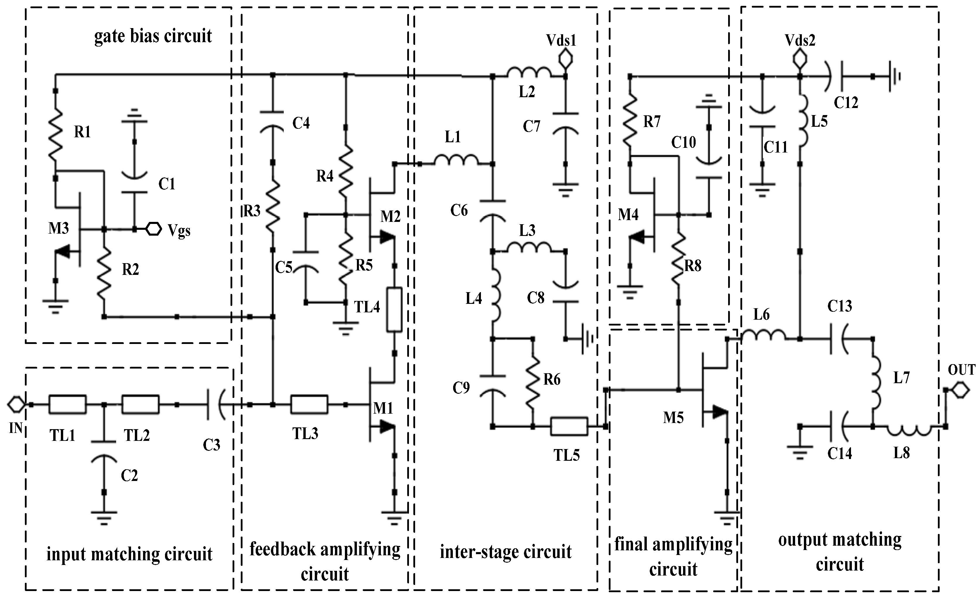
2.1. Design of MMIC PA

In this paper, a GaAs pHEMT high gain MMIC PA is used as the object to do temperature performance investigation. The circuit schematic for this MMIC PA is shown in Figure 1. This MMIC PA is composed of input matching circuit, gate bias circuit, feedback amplifying circuit, inter-stage matching circuit, final amplifying circuit, and output matching circuit. Among them, the transistors M1 and M2 with cascode structure are used in the feedback amplifying circuit. The influence of Miller effect on broadband reduces by this structure, which makes the circuit achieve the characteristics of high gain, wide bandwidth, and high linearity [20,21]. Moreover, the common source structure in the final amplifying circuit is combined with the broadband RC matching network to realize the broadband output matching and high power characteristics [22,23]. Besides, the gate bias circuit is mainly composed of transistor M3, rectification resistance R1, rectification resistance R2, and bypass capacitor C1. This design aims to optimize the gain compression, linear distortion, and temperature sensitivity of MMIC PA. During the above circuit analysis, the Advanced Design System (ADS) is utilized to design and optimize circuit. Firstly, according to applications, the type of transistor and stage for PA is defined. Moreover, the DC sweep, stability analysis, bias circuit design, load-pull, and source-pull are implemented by ADS in turn. Meanwhile, the simulation schematic of this MMIC PA is simulated and optimized after the actual elements are added. Then, the layout shown in Figure 2 is achieved.

2.2. Simulation Results of MMIC PA

After the layout is generated, the performance of this MMIC PA needs to be simulated and optimized again. Among them, the simulated results of S-parameters are shown in Figure 3. It can be seen that in the frequency range of 2.4–4.4 GHz, S21 is close to 30.2 dB, the input return loss (S11) is less than −13 dB, and output return loss (S22) is smaller than −6 dB.
Moreover, the simulated result of stability factor is shown in Figure 4. It is clear to find that the stability factor is greater than 1, which indicates that the PA is absolutely stable in the whole frequency band.
At the same time, the simulated results of output power (Pout) and gain are shown in Figure 5. It can be seen that the Pout and gain is up to 27.2 dBm and 30.4 dB, respectively. As the input power (Pin) increases, the phenomenon of gain compression is presented. When gain is compressed by 1 dB, the Pin is −2 dBm, and the corresponding Pout is 27 dBm.
All in all, the simulation results of MMIC PA have been shown. Although S11 and S22 are larger than −10 dB in partial frequency bands, the performance still meets the requirements for 5G. This is because 3.6 GHz is extremely important in 5G applications. The performance in other frequencies can be appropriately compromised. The poor S11 and S22 are the compromise victim for OIP3. Finally, the PA is made if the performance meets design requirements. The photograph and experiment fixture for this MMIC PA are shown in Figure 6. It can be shown that its size is only 1.3 mm × 1 mm.

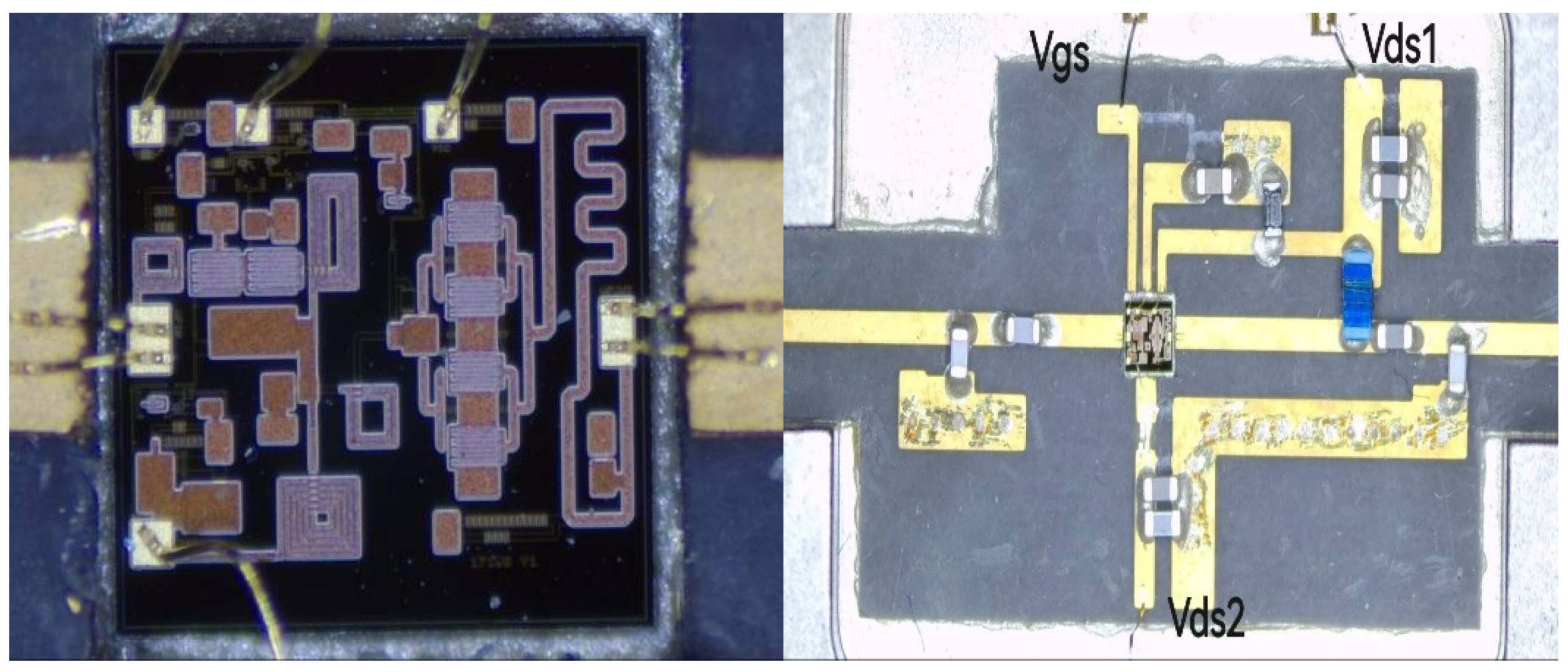
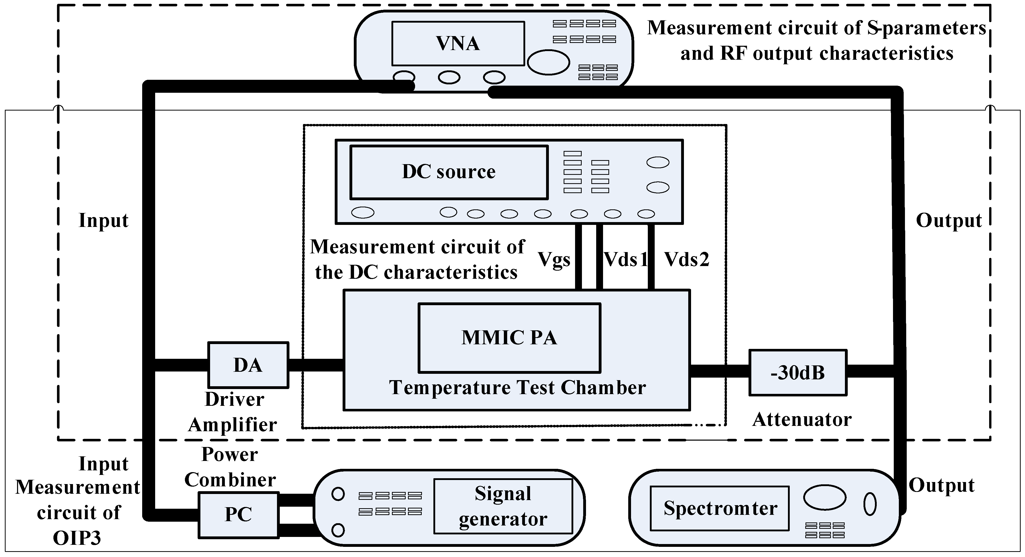
3. Experimental Setup

To realize temperature investigation for this MMIC PA, the DC characteristics, S-parameters, RF output characteristics, and OIP3 are measured at −40 °C, −20 °C, 0 °C, 25 °C, 50 °C, 75 °C, 100 °C, and 120 °C, respectively. The measurement circuits of this MMIC PA are shown in Figure 7. During the experiments, this MMIC PA is placed in the temperature test chamber at different temperatures with DC power. The drain–source voltage ( V ds ) is 5 V and the gate–source voltage ( V gs ) is 1.8 V. While measuring S-parameters and RF output characteristics, the vector network analyzer (VNA) ZNB-8 is used. Meanwhile, to achieve the maximum output power of PA, it is necessary to add a driver amplifier (DA) at the input terminal of this PA. Moreover, its output terminal is connected with an attenuator of −30 dB to ensure the safe use of instruments. During measuring OIP3, the vector signal generator SMW200A and spectrometer FSW of ROHDE & SCHWARTZ are employed. The dual-tone signals are input through a power combiner (PC). The experimental environment is shown in Figure 8.

4. Experimental Results and Discussions

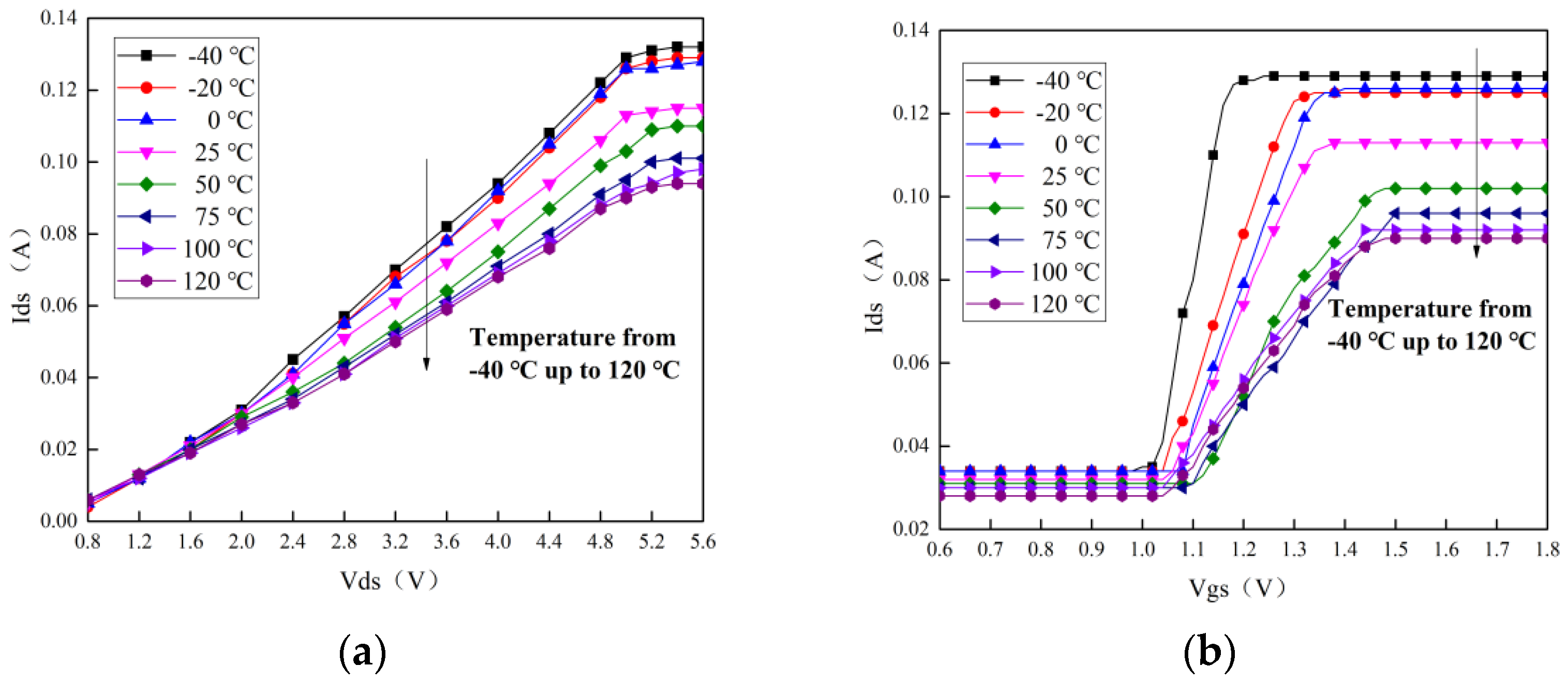
4.1. The DC Characteristics Measurement and Discussions

The measured curves of output characteristic and transfer characteristic for GaAs pHEMT with the rising temperature are shown in Figure 9. It can be seen that the saturation I ds at RT is 112 mA. When the temperature rises from −40 °C to 120 °C, the I ds reduces about 38 mA with the increasing V ds and V gs . The reason for this phenomenon is that the two-dimensional electron gas (2DEG) in the channel of GaAs pHEMT is moved to the buffer layer with the rising temperature, which reduces μ . Next, the I ds degrades [11,24]. Meanwhile, the thermal conductivity of GaAs pHEMT is relatively low [25]. The heat generated by the self-heating effect cannot be dissipated in time. As a result, the lattice scattering mechanism greatly enhances and leads to a decrease in μ . Ultimately, the I ds significantly decreases. Moreover, with the enhancement of lattice scattering mechanism, the self-heating effect becomes more significant [26]. Apart from the above, the trapping ability of surface traps to channel electrons also enhances with the rising temperature, which causes a significant decrease in I ds . In short, the DC characteristics for GaAs pHEMT markedly degrade with the rising temperature, which further drops the transistor performance.
The studies show that the DC characteristics for GaAs pHEMT are expressed as [27]:
I ds = μ d W L V ds ( V gs V T 1 2 V ds ) V ds < V gs V T 1 2 μ d W L V gs V T 2 V ds V gs V T  
μ T 3 / 2
where W and L represent the gate width and gate length, respectively, is dielectric coefficient, d is the thickness, T refers to the ambient temperature, V T is the threshold voltage. Moreover, the influence of V T on I ds can be neglected [14]. Thus, the key reason causing the degradation for I ds is the reduction in μ . In fact, generally for power transistors, L is not a designable parameter. The degradation for I ds caused by the reduction in μ can be compensated by increasing W . However, the drain–source junction area expands by increasing the W . In summary, the compromise choice for W can be made to realize the temperature compensation for the DC characteristics.

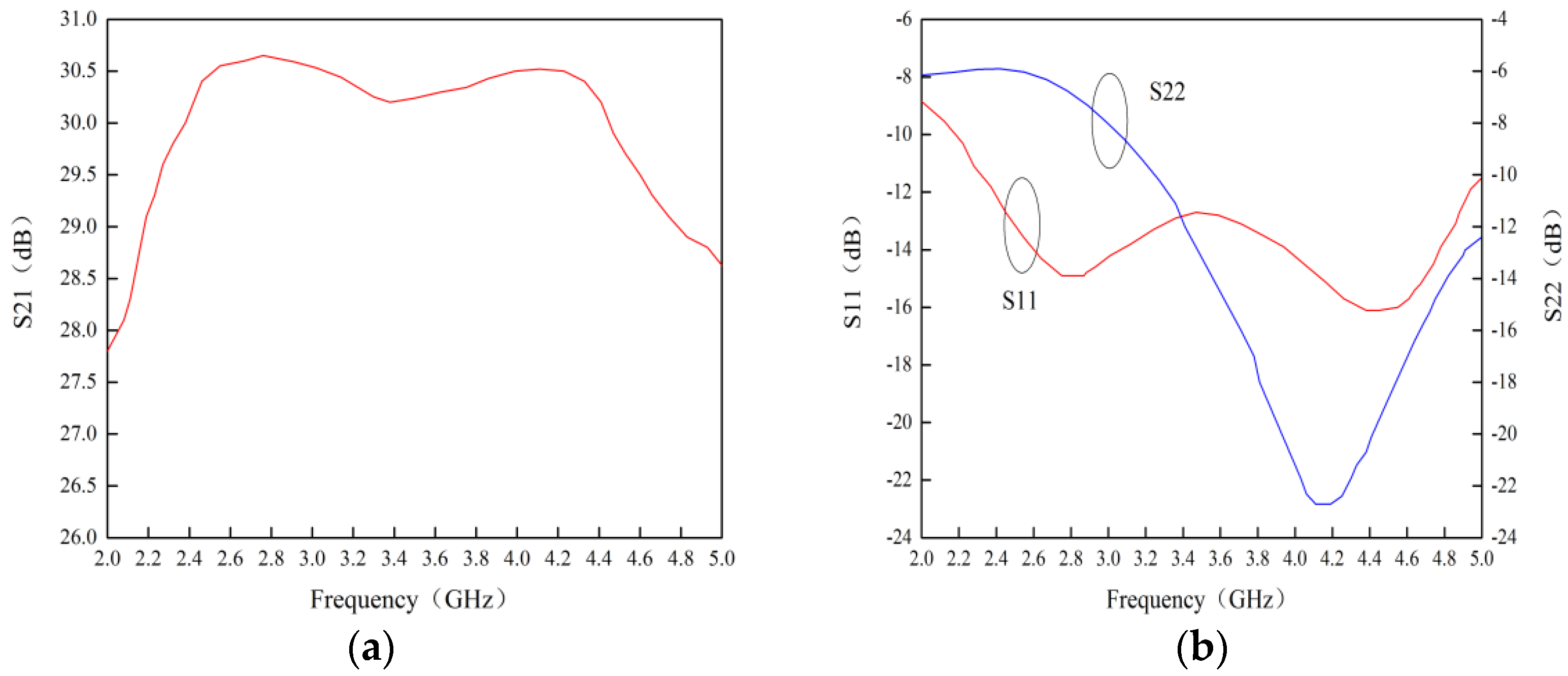
4.2. S-Parameters Measurement and Discussions

The measured curves of S-parameters for this MMIC PA with rising temperature are shown in Figure 10. It can be seen that S21 is up to 26.47 dB at RT. When the temperature rises from −40 °C to 120 °C, S21 gradually decreases, and the maximum reduction is about 4.75 dB. This is due to the decrease of g m caused by increasing temperature, which leads to the degradation of S21 [28,29]. Furthermore, the input return loss (S11) and output return loss (S22) also reduce. As temperature rises, S11 and S22 are overlapped due to mismatch of circuit impedance in the frequency band ranges of and 3.4–3.8 GHz and 4.0–4.4 GHz, respectively. However, in the frequency range of 2.4–4.4 GHz, S21 is greater than 22 dB, S11 and S22 are less than –5 dB. Meanwhile, S11 and S22 are still smaller than –10 dB in 3.6 GHz. These results indicate that S-parameters for this MMIC PA remain stable with the rising temperature.
It has been proved that g m is expressed as [27]:
g m = μ d W L V ds V ds < V gs V T   μ d W L V gs V T V ds V gs V T  
It can be seen from Equation (3) that when the temperature rises, g m drops because of the reduction in μ . Finally, S21 decreases. Therefore, S21 can be improved by making the compromise choice for W . Furthermore, studies [18] have shown that S21 can also be compensated effectively by a temperature compensation circuit with stacked structure in 2020.

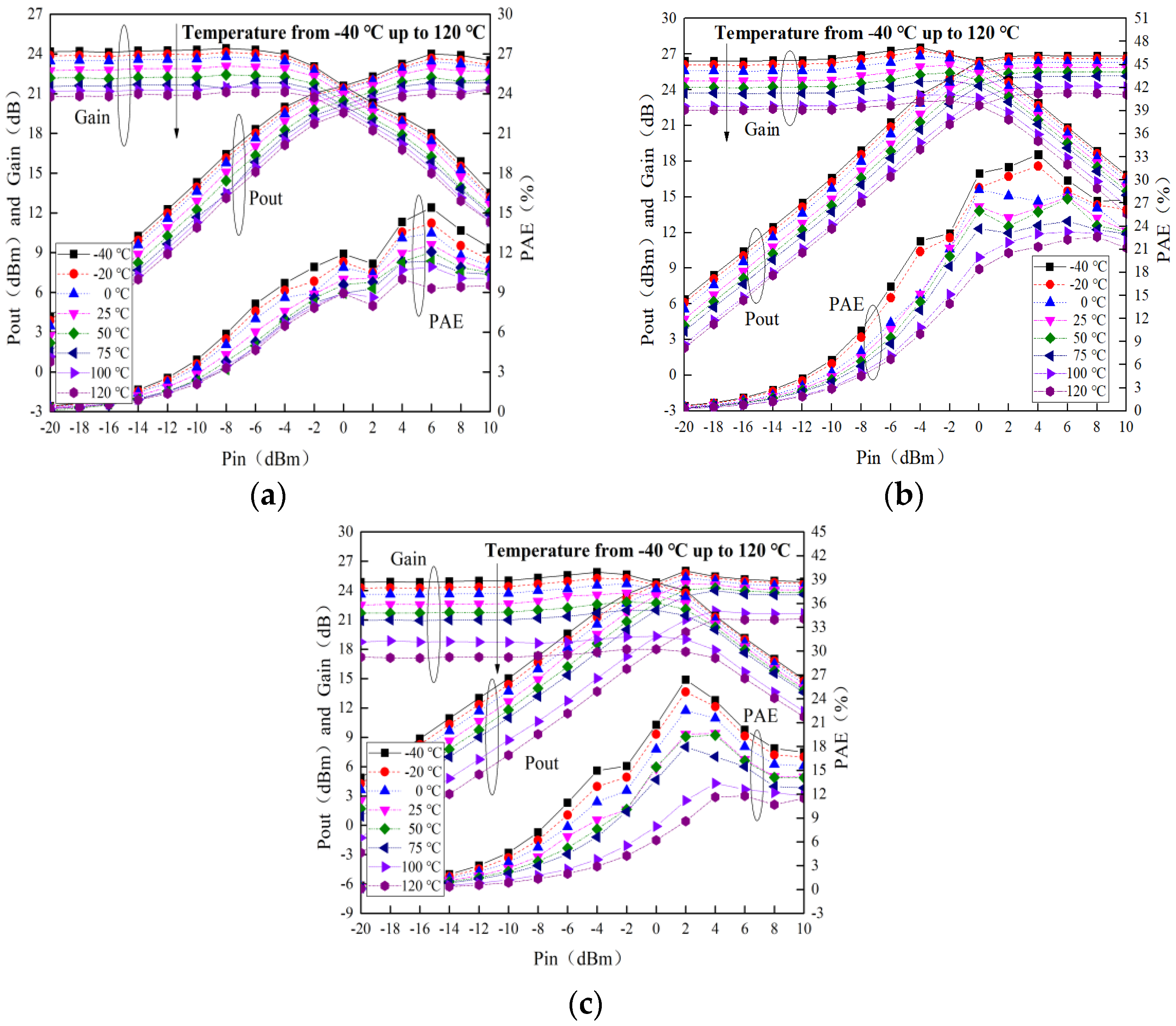
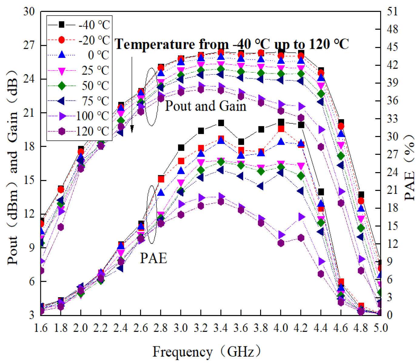
4.3. RF Output Characteristics Measurement and Discussions

The measured curves of RF output characteristics for this MMIC PA with the rising temperature are shown in Figure 11 and Figure 12, respectively. It can be seen that the Pout, gain, and power added efficiency (PAE) degrade with the increasing temperature. When the frequency is 3.4 GHz, the saturated Pout at room temperature is 25.87 dBm, the saturated gain is 24.83 dB, and the maximum PAE is 27.82%. Due to the rising temperature, the Pout, gain, and PAE drop about 3.24 dBm, 4.11 dB, and 12.01%, respectively. When the Pin is 0 dBm, the Pout and PAE decline about 5.22 dBm and 20.32%, respectively. This is due to the truth that the R ds has certain impact on Pout [28,29]. R ds elevates with the rising temperature, resulting in more power dissipation inside the MMIC PA. Moreover, R ds is represented as [30]:
R ds = V ds I ds = 1 μ d W L ( V gs V T V ds )
According to Equation (4), as temperature rises, R ds increases due to the reduction in μ . Besides, gain and PAE are as follows [14,31]:
Gain = Pout Pin
PAE = Pin Gain 1 P dc
where Pdc is the DC power. It is clear to find from Equation (5) that as temperature rises, gain also decreases because of the reduction in μ . Meanwhile, Pdc increases after thermal storage [31]. Thus, PAE reduces with the rising temperature according to Equation (6). In a word, when the temperature rises, the RF output characteristics for this MMIC PA degrade severely due to the reduction in μ .
It can be seen from the previous analysis [28,29] that R ds is the key factor to determine the temperature performance of RF output characteristics. The variation of R ds is closely related to μ . Thus, it is necessary to choose the reasonable W to reduce power dissipation. Meanwhile, the RF output characteristics can be effectively improved through a temperature compensation circuit [18]. Besides, reducing the density of surface state and surface trap is also a feasible way [32]. Firstly, it is available to avoid new surface traps in the design process. Then, the surface needs to be properly treated to make the density at a reasonable level.

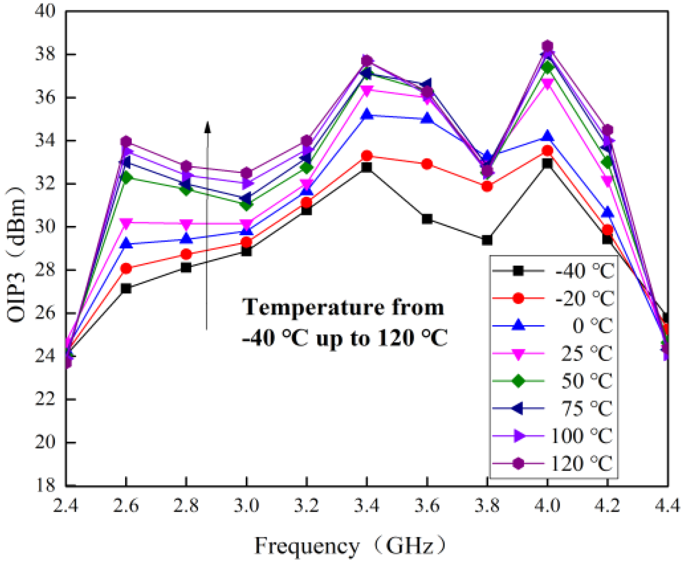
4.4. OIP3 Measurement and Discussions

The measured curves of OIP3 for this MMIC PA with rising temperature are shown in Figure 13. It can be seen that the maximum OIP3 is 36.69 dBm at RT in the range of 2.4–4.4 GHz. Furthermore, OIP3 increases with the rising temperature. The fundamental reason for the above phenomenon is related to circuit design. First of all, OIP3 increases due to transistors M1 and M2 used in the feedback amplifying circuit. Secondly, when this MMIC PA works at the suitable bias circuit, the voltage and current flowing through transistor M3 increase. Eventually, the distortion for OIP3 is improved by this behavior. Studies have [33] shown that when OIP3 increases, the wires are easy to be short-circuited or broken, which directly affects the lifetime for this MMIC PA. Finally, it is reported that the lifetime can be prolonged by designing a reasonable layout with multi-layer structure, controlling the process strictly.
It is worth noting that there is an error between the simulation and measurement results. This is due to the parasitic effects of the capacitances, inductances, resistances, and microstrip lines in the fixture. Moreover, the difference is also influenced by the device process and bond wires, which has an impact for matching networks [34]. This difference is within the reasonable range for PA design.

5. Conclusions

In this paper, a series of temperature character tests have been carried out for this MMIC PA in the temperature range of −40 °C–120 °C. It can be seen that the DC characteristics, S21, and RF output characteristics for this MMIC PA all reduce, and OIP3 increases with the rising temperature. Through the analysis, it is found that when the temperature rises, the reduction in μ and special circuit design are the key reasons leading to the above temperature behavior. In view of the above phenomenon, it is concluded that the performance of this MMIC PA can be improved by choosing the compromise W , designing temperature compensation circuit, reducing the density of surface state and surface trap, optimizing layout design, and so on. The investigation is vital for RF microwave circuits in the future.

Author Contributions

Conceptualization, L.J.; methodology Q.L.; validation X.W.; investigation, L.J. and Q.L.; resources, H.W.; writing—original draft preparation, L.J.; writing—review and editing, Q.L. and H.W. All authors have read and agreed to the published version of the manuscript.

Funding

This research was funded by the National Natural Science Foundation (62161046), the West Light Youth Talent Program of the Chinese Academy of Sciences (1_14), the Natural Science Foundation of Qinghai Province (2021-ZJ-910) and the Innovative Program of Qinghai Minzu University (10M2021009).

Data Availability Statement

The data presented in this study is available on request from the corresponding author.

Conflicts of Interest

The authors declare no conflict of interest.

References

  1. Zhang, C.; Wang, H.; Zhang, J.; Du, G.; Yang, J. Failure Analysis on Damaged GaAs HEMT MMIC Caused by Microwave Pulse. IEEE Trans. Electromagn. Compat. 2014, 56, 1545–1549. [Google Scholar] [CrossRef]
  2. Ketterson, A.A.; Masselink, W.T.; Gedymin, J.S.; Klem, J.; Peng, C.K.; Kopp, W.F.; Morkoc, H.; Gleason, K.R. Characterization of InGaAs/AlGaAs pseudomorphic modulation-doped field-effect transistors. IEEE Trans. Electron Devices. 1986, 33, 564–571. [Google Scholar] [CrossRef]
  3. Peng, Y.Y.; Lu, K.J.; Sui, W.Q. A 7- to 14-GHz GaAs pHEMT LNA with 1.1 dB noise figure and 26 dB gain. Microw. Opt. Technol. Lett. 2010, 52, 2615–2617. [Google Scholar] [CrossRef]
  4. Gu, J.; Fu, H.; Na, W.; Zhang, Q.; Ma, J. Fast and Automated Electromigration Analysis for CMOS RF PA Design. J. Electron. Test. 2017, 33, 133–140. [Google Scholar] [CrossRef]
  5. Wu, H.F.; Liao, X.J.; Lin, Q.; Hua, Y.N.; Wang, C.T.; Cheng, Y.J.; Hu, L.L.; Lv, J.P. A Compact Ultrabroadband Stacked Traveling-Wave GaN on Si Power Amplifier. IEEE Trans. Microw. Theory Tech. 2018, 66, 3306–3314. [Google Scholar] [CrossRef]
  6. Guo, S.C. Design and Performance Degradation Assessment of the Radio Frequency Power Amplifier Chip. Master’s Thesis, Tianjin University, Tianjin, China, 2018. [Google Scholar]
  7. Lin, Q.; Cheng, Q.F.; Gu, J.J.; Zhu, Y.Y.; Chen, C.; Fu, H.P. Design and Temperature Reliability experimenting for A 0.6–2.14 GHz Broadband Power Amplifier. J. Electron. Test. 2016, 32, 235–240. [Google Scholar] [CrossRef]
  8. Zhou, S.H. Experimentally investigating the degradations of small-signal gain for a GaN class-AB dual-band power amplifier under high temperature and humidity conditions. AIP Adv. 2020, 10, 125219. [Google Scholar] [CrossRef]
  9. Lin, Q.; Wu, H.; Li, X. Study of temperature reliability for a parallel high-efficiency class-E power amplifier. Circuit World. 2017, 43, 111–117. [Google Scholar] [CrossRef]
  10. Zhou, S.H.; Wang, J. An RF Stress-Based Thermal Shock Test Method for a CMOS Power Amplifier. IEEE J. Electron Devices Soc. 2021, 9, 1024–1029. [Google Scholar] [CrossRef]
  11. Alim, M.A.; Rezazadeh, A.A. Thermal Influence on Multibias Small- and Large-Signal Parameters of GaAs pHEMT Fabricated in Multilayer 3-D MMIC. IEEE Trans. Electron Devices. 2017, 64, 1511–1518. [Google Scholar] [CrossRef]
  12. Giovanni, C.; Gustavo, A.; Antonio, R.; Pawel, B. Investigation on the thermal behavior of microwave GaN HEMTs. Solid-State Electron. 2011, 64, 28–33. [Google Scholar]
  13. Li, C.Y. Evaluation of temperature dependence and lifetime of 79 GHz power amplifier. In Proceedings of the IEEE International Meeting for Future of Electron Devices, Suita, Japan, 5–6 June 2013; pp. 100–101. [Google Scholar]
  14. He, Z.; Zhou, S.H.; Nie, M.N. Experimentally investigating the performance degradations of the CMOS PA at different temperatures. AIP Adv. 2021, 11, 115205. [Google Scholar] [CrossRef]
  15. Medra, A.; Giannini, V.; Guermandi, D.; Wambacq, P. A 79 GHz variable gain low-noise amplifier and power amplifier in 28 nm CMOS operating up to 125 °C. In Proceedings of the 40th European Solid State Circuits Conference (ESSCIRC), Venice Lido, Italy, 22–26 September 2014; pp. 183–186. [Google Scholar]
  16. Huang, J.C.; Hsu, W.C.; Lee, C.S.; Chang, W.C.; Huang, D.H. Improved high-temperature characteristics of a symmetrically graded AlGaAs/InxGa1−xAs/AlGaAs pHEMT. Semicond. Sci. Technol. 2016, 21, 1675. [Google Scholar] [CrossRef]
  17. Cardoso, A.S.; Omprakash, A.P.; Chakraborty, P.S.; Karaulac, N.; Fleischhauer, D.M. On the Cryogenic RF Linearity of SiGe HBTs in a Fourth-Generation 90-nm SiGe BiCMOS Technology. IEEE Trans. Electron Devices 2015, 62, 1127–1135. [Google Scholar] [CrossRef]
  18. Wei, S.Z.; Wu, H.F.; Zhang, M.Z. Design of Ka-band and CMOS stacked power amplifier with temperature compensation. Chin. J. Radio Sci. 2020, 35, 715–720. [Google Scholar]
  19. Park, J.; Lee, J.; Yun, T. High-Linearity Drive Amplifier Using Active Local Feedback. IEEE Microw. Wirel. Compon. Lett. 2016, 26, 613–615. [Google Scholar] [CrossRef]
  20. Wu, H.F.; Lin, Q.; Zhu, L.; Chen, S.J.; Chen, Y.J.; Hu, L.L. A 2 to 18 GHz Compact High-Gain and High-Power GaN Amplifier. In Proceedings of the IEEE MTT-S International Microwave Symposium (IMS), Boston, MA, USA, 2–7 June 2019; pp. 710–713. [Google Scholar]
  21. Kim, Y.; Kwon, Y. Analysis and Design of Millimeter-Wave Power Amplifier Using Stacked-FET Structure. IEEE Trans. Microw. Theory Tech. 2015, 63, 691–702. [Google Scholar] [CrossRef]
  22. Hu, L.L.; Hu, D.H.; Wu, H.F.; Lin, Q.; Hua, Y.N.; Chen, S.W.; Zhang, X.M. An Ultra-wideband GaAs pHEMT Distributed Power Amplifier. In Proceedings of the IEEE 4th Advanced Information Technology, Electronic and Automation Control Conference (IAEAC), Chengdu, China, 20–22 December 2019; pp. 2144–2147. [Google Scholar]
  23. Gavel, M.; Angelov, I.; Ferndahl, M.; Zirath, H. A high voltage mm-wave stacked HEMT power amplifier in 0.1 µm InGaAs technology. In Proceedings of the IEEE MTT-S International Microwave Symposium (IMS), Phoenix, AZ, USA, 17–22 May 2015; pp. 1–3. [Google Scholar]
  24. Lin, Y.S.; Chen, B.Y. Performance of AlGaAs/InGaAs/GaAs Pseudomorphic High Electron Mobility Transistor as a Function of Temperature. J. Electrochem. Soc. 2007, 154, 406–411. [Google Scholar] [CrossRef]
  25. Rezaei, S.; Belostotski, L.; Ghannouchi, F.M.; Aflaki, P. Integrated Design of a Class-J Power Amplifier. IEEE Trans. Microw. Theory Tech. 2013, 61, 1639–1648. [Google Scholar] [CrossRef]
  26. Alim, M.A.; Chowdhury, A.Z.; Islam, S.; Gaquiere, C.; Crupi, G. Temperature-Sensitivity of Two Microwave HEMT Devices: AlGaAs/GaAs vs. AlGaN/GaN Heterostructures. Electronics 2021, 10, 1115. [Google Scholar] [CrossRef]
  27. Chen, Z. Research and Design of Ku Band Power Amplifier. Master’s Thesis, Guangdong University of Technology, Guangzhou, China, 2019. [Google Scholar]
  28. Alim, M.A.; Rezazadeh, A.A. Device behaviour and zero temperature coefficients analysis for microwave GaAs HEMT. Solid-State Electron. 2018, 147, 13–18. [Google Scholar] [CrossRef]
  29. Gryglewski, D.; Wojtasiak, W.; Kaminska, E.; Piotrowska, A. Characterization of self-Heating process in GaN-based HEMTs. Electronics 2020, 9, 1305. [Google Scholar] [CrossRef]
  30. Matheoud, V.; Sahin Solmaz, N.; Boero, G. A Low-Power Microwave HEMT LC Oscillator Operating Down to 1.4 K. IEEE Trans. Microw. Theory Tech. 2019, 67, 2782–2792. [Google Scholar] [CrossRef]
  31. Zheng, J.X. Modeling of AlGaN/GaN Based HEMT and Its Application in Power Amplifier. Ph.D. Thesis, Xidian University, Xi’an, China, 2018. [Google Scholar]
  32. Menozzi, R. Hot electron effects and degradation of GaAs and InP HEMTs for microwave and millimetre-wave applications. Semicond. Sci. Technol. 1998, 13, 1053. [Google Scholar] [CrossRef]
  33. Lin, Q.; Wu, H.F.; Chen, S.J.; Jia, G.Q.; Chen, C. Study of complete interconnect reliability for a GaAs MMIC power amplifier. Int. J. Electron. 2018, 105, 794–805. [Google Scholar] [CrossRef]
  34. Çağlar, A.; Yelten, M.B. Design of Cryogenic LNAs for High Linearity in Space Applications. IEEE Trans. Circuits Syst. I-Regul. Pap. 2019, 66, 4619–4627. [Google Scholar] [CrossRef]
Figure 1. The circuit schematic of this MMIC PA.
Electronics 11 01669 g001
Figure 2. The layout of this MMIC PA.
Electronics 11 01669 g002
Figure 3. Simulated curves of S-parameters: (a) S21; (b) S11 and S22.
Electronics 11 01669 g003
Figure 4. Simulated curve of stability factor.
Electronics 11 01669 g004
Figure 5. Simulated curves of RF output characteristics (a) Pout; (b) gain.
Electronics 11 01669 g005
Figure 6. The photograph and experiment fixture of MMIC PA.
Electronics 11 01669 g006
Figure 7. Measurement circuits of MMIC PA.
Electronics 11 01669 g007
Figure 8. Experimental environment of MMIC PA.
Electronics 11 01669 g008
Figure 9. Measured DC characteristics curves of the GaAs pHEMTat different temperatures: (a) the output characteristic; (b) the transfer characteristic.
Electronics 11 01669 g009
Figure 10. Measured curves of S-parameters at different temperatures: (a) S21; (b) S11; (c) S22.
Electronics 11 01669 g010
Figure 11. Measured curves of RF output characteristics at different temperatures: (a) 2.4 GHz; (b) 3.4 GHz; (c) 4.4 GHz.
Electronics 11 01669 g011
Figure 12. Measured curves of RF output characteristics with Pin of 0 dBm at different temperatures.
Electronics 11 01669 g012
Figure 13. Measured curves of OIP3 at different temperatures.
Electronics 11 01669 g013
Publisher’s Note: MDPI stays neutral with regard to jurisdictional claims in published maps and institutional affiliations.

