Article

Receiver Analog Front-End Cascading Transimpedance Amplifier and Continuous-Time Linear Equalizer for Signals of 5 to 30 Gb/s

by
Pragada Venkata Satya Challayya Naidu
and
Chih-Wen Lu
*
Department of Engineering and System Science, National Tsing Hua University, Hsinchu 300044, Taiwan
*
Author to whom correspondence should be addressed.
Electronics 2022, 11(10), 1546; https://doi.org/10.3390/electronics11101546
Submission received: 15 March 2022 / Revised: 29 April 2022 / Accepted: 2 May 2022 / Published: 12 May 2022

Abstract

:
A 5–30 Gb/s receiver analog front-end (AFE) cascading transimpedance amplifier (TIA) and continuous-time linear equalizer (CTLE) were implemented using a Taiwan Semiconductor 180 nm process. The system comprises a two-stage differential input pair CTLE, TIA, and a differential termination resistor Rm. A source-degenerated transconductance stage was adopted in the CTLE, and source follower and shunt feedback resistor stages were adopted in the TIA. The proposed CTLE could achieve high frequencies by altering the tail current with fixed degenerate capacitance CS and resistance RS. The proposed AFE achieved high bandwidth, and the use of a feedback resistor Rf and inductor Lf improved its high-frequency performance. Simulation results revealed that the CTLE can compensate for 16 dB of channel loss at a 3 GHz Nyquist frequency and can open closed eyes in a 6 Gb/s non-return-to-zero signal with a bit error rate of 0.16 × 10⁻¹² for a 231 − 1 pseudorandom binary sequence input. The AFE could compensate for 12 dB of channel loss at a 15 GHz Nyquist frequency and can open closed eyes in a 30 Gb/s PAM4 signal from a pseudorandom binary sequence input; it consumed 27 mW of power at 1.8 V.

1. Introduction

As data rates have increased by 1.5 times every year since 2000, high-speed data communications are required in modern broadband applications to address bandwidth demand. Initially, in 2000, radio frequency applications required a bandwidth of 1–2 GHz for optical time-domain reflectometer applications. To meet modern broadband demand, data rates have increased to 25~30 Gbps, which is more than 75% of previous data communications. Increasing bandwidth must meet multiple challenges including channel loss, high-speed operation, area, equalization, and robustness. For data communication power, in particular, consumption is a very important factor in maintaining high performance. There are several previous studies of 28 Gbps or higher data rates [1,2,3,4,5]. Those use unrolled decision feedback equalizers to meet critical timing margins, but the unrolled CTLE structure increases the power and die’s area. To achieve these challenges, one of the key designs is an analog front-end (AFE) cascading transimpedance amplifier with a continuous-time linear equalizer.
Historically, TIAs have been mostly developed for the front-ends of the optical receivers (for example, the families of 2.5, 10, 40, … GB/s). However, their usage is not limited to optical applications, although they have been for a long time the major driving force beyond development towards both lower noise and higher speeds. Nevertheless, in recent decades, advanced TIA designs have become increasingly popular for a variety of applications such as physics and radiation detectors of particles, miniaturized magnetic resonance spectroscopy [2], and vision and biological sensors. Different applications have their own requirements for the main parameters of TIA design. For example, high-speed optical communication circuits have pushed the bandwidth of TIAs in multiple GHz ranges from novel designs with lower power consumption to reduced chip area and minimized noise while operating at significant frequency [6]. Obviously, the front-end TIA is the most critical component of the channel influencing both noise sensitivity and the speed of the overall system. At the output of the linear channel, voltage is provided that can be later used by decision circuits.
The second most critical component of the analog front-end block is the decision circuit or equalization circuit as shown in Figure 1. Equalization is typically implemented in both the transmitter and the receiver [7]. Before the channel, it is desirable to “peak” the transmitted high-frequency content instead of performing all the high-frequency peaking at the receiver side. On the receiver side, high-frequency peaking degrades the receiver input signal-to-noise ratio (SNR), whereas the transmit side does not. Therefore, within the transmitter, equalization is implemented to supply pre-emphasis of the high-frequency vanguard of bit transitions. In the receiver, equalization is implemented to revive the combined transmitter and channel characteristics towards a reference channel that has no or reduced ISI. Obviously, CTLE in a receiver is intended to equalize the combined characteristics of the transmitter and channel and remove the ISI at the received signal sampling points. The RX CTLE is similar to TX FFE CTLE except the input is an analog signal. The RX CTLE is often called a discrete-time linear equalizer [3,8]. As an FIR filter, designed to subtract ISI effects from adjacent bits. The output of RX CTLE is further sampled to point per data time interval for data detection. The RX CTLE will only cancel ISI at the data detection sample points.
Channel losses or insufficient bandwidth are obstacles to achieving higher data rates in data communications. One solution is changing the signal transformation scheme from two-level pulse amplitude modulation (PAM2), also known as non-return-to-zero (NRZ), to four-level pulse amplitude modulation (PAM4), to double the data rate without increasing the bandwidth [9,10]. However, PAM4 requires greater system linearity. Increasing system bandwidth or using a continuous-time linear equalizer (CTLE) to compensate for channel losses are other potential solutions [11,12,13].
Receivers with equalization can overcome problems caused by channel loss, such as intersymbol interference. Effective high-performance receivers must meet numerous requirements, including those for power consumption, area, bit error rate (BER), and equalization. In receiver analog front-ends (AFEs), equalizers such as CTLE are commonly used (Figure 1). CTLE has lower power consumption than other equalizers in high-speed applications. Moreover, as the data rate increases, the proposed CTLE can achieve different equalization for different cable lengths by tuning the tail current with a fixed capacitor and resistor. The architecture presented in [1] is generally used in high-speed AFEs.
Typically, transimpedance amplifiers (TIAs) are used to limit receiver noise. Common-gate stages are effective amplifiers for high frequencies but have poor noise characteristics [14,15]. The TIAs based on the shunt–feedback architecture have a low-noise topology that is advantageous for high-data-rate applications. However, a trade-off exists between the performance of the circuit and the suitability of the DC operating point in conventional linear transconductance (Gm)-TIA systems. To achieve a suitable DC operating point, the size of the transistors must be increased, resulting in a large parasitic capacitance at the output nodes and reducing the bandwidth of the circuit. To overcome this problem, source follower (SF) stages were used to design the proposed AFE. This paper is organized as follows: Section 2 details the design considerations, Section 3 presents the simulation results, and Section 4 concludes the research.

2. Design Consideration
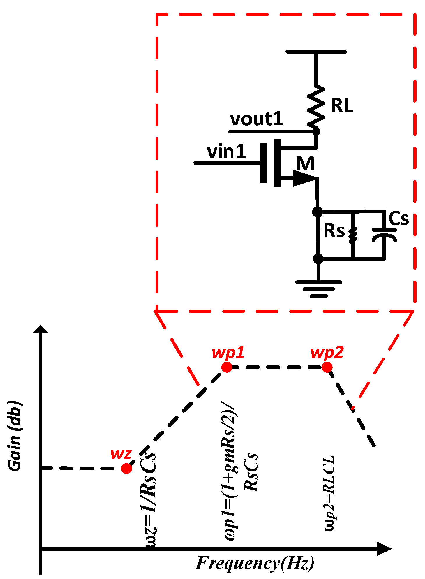
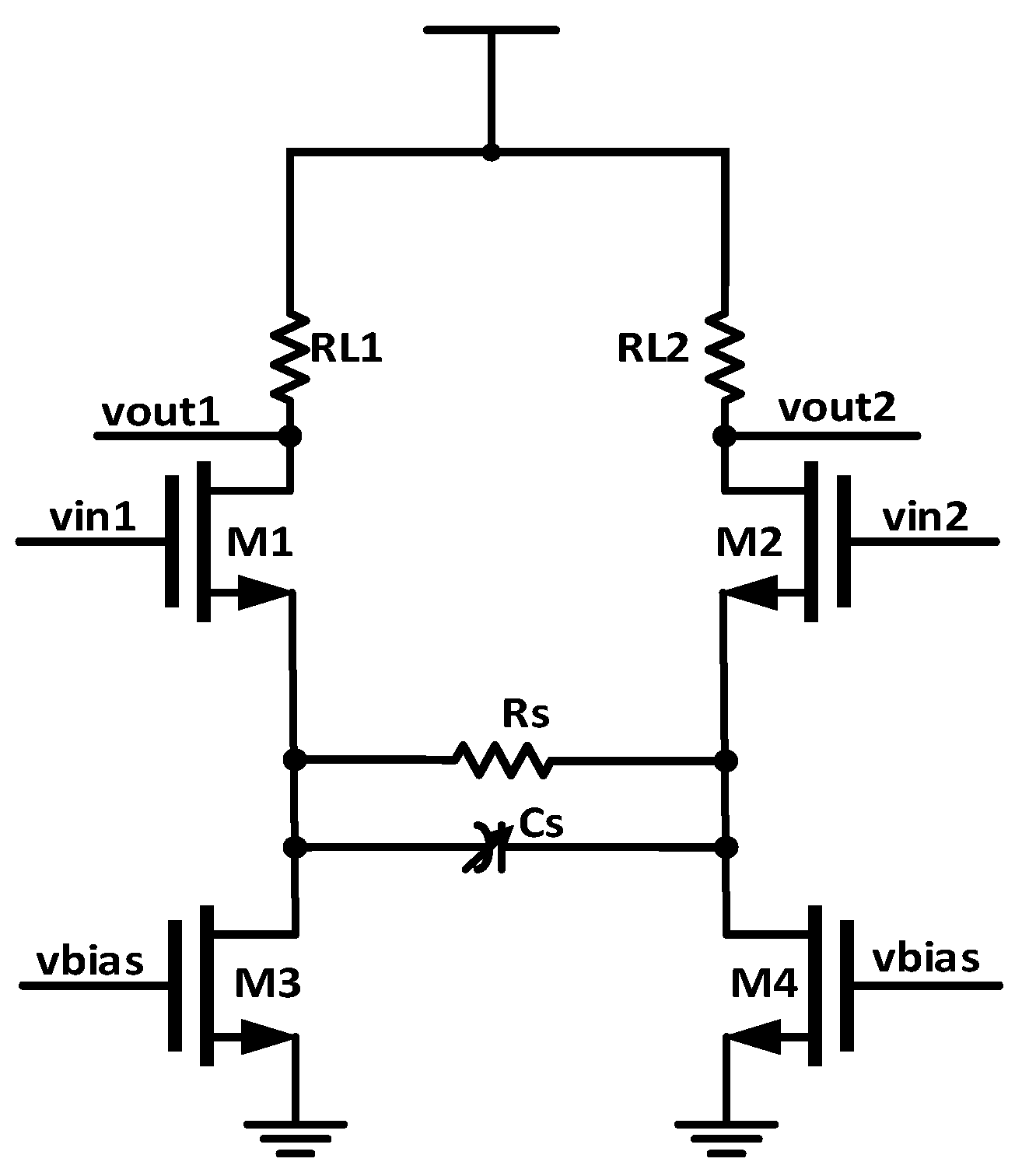
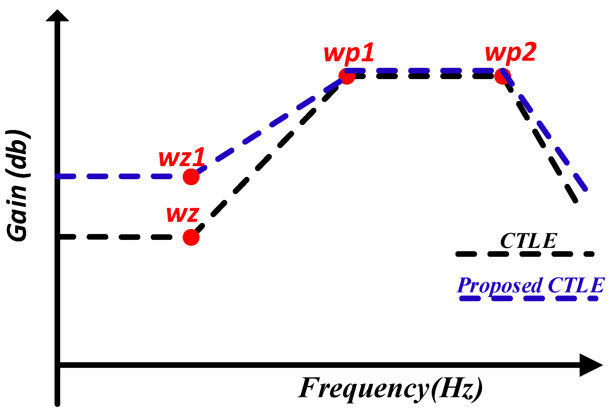
2.1. CTLE

The equalization value of conventional CTLEs can be increased or decreased by varying the capacitor (CS) and resistor (RS), illustrated in the schematic in Figure 2. The peaking frequency is directly correlated with this equalization value and affects the bandwidth fw. Consequently, disassociating the equalization value and fw in the circuit is key. The source-degenerated Gm-cell is chosen such that the gain is degenerated through RS, ensuring sufficient linearity in the system (Figure 2). A zero can also be introduced by combining CS and RS [8,16].
Equation (1) presents the transfer function of the single-ended CTLE.
H   ( S ) = G M R L 1 + G M R S 2   ×   1 + S ω z ( 1 + S ω p 1 ) ( 1 + S ω p 2 )
where ω z = 1 R s C s , ω p 1 = 1 + G M R s 2 R s C s ,   and   ω p 2 = 1 R L C L are the zero and two poles of the CTLE, respectively (Figure 3).
To attain the peak gain at a higher frequency, the CTLE must be designed such that the pole frequency is higher than the zero frequency [17,18,19]. The peaking gain also depends on the dominant pole and zero. The frequencies depend on GM of the differential pair and of the degeneration CS and RS, as presented in Equation (2).
Maximum   boost   peaking = ω p 1 ω z = 1 + G M R s .
In the low-frequency range, CTLE operates similarly to a differential amplifier with source degeneration, and their gains are therefore equal in this range:
DC   gain = g m R L 1 + G M R s 2
In the high-frequency range, CS shorts the pins of the CTLE, and the circuit operates similarly to a differential amplifier without source degeneration. Therefore, the peak gain of the CTLE is as follows:
peak   gain = g m R L
Figure 2 reveals that if V b i a s varies, the current flow through transistors M1 and M2 varies. However, the output current at nodes V o u t 1 and V o u t 2 changes drastically, and the dominant poles and zero also change slightly. To achieve constant current flow at nodes V o u t 1 and V o u t 2 while enabling variation in V b i a s , a two-stage differential input pair CTLE with fixed degeneration CS and RS is proposed.

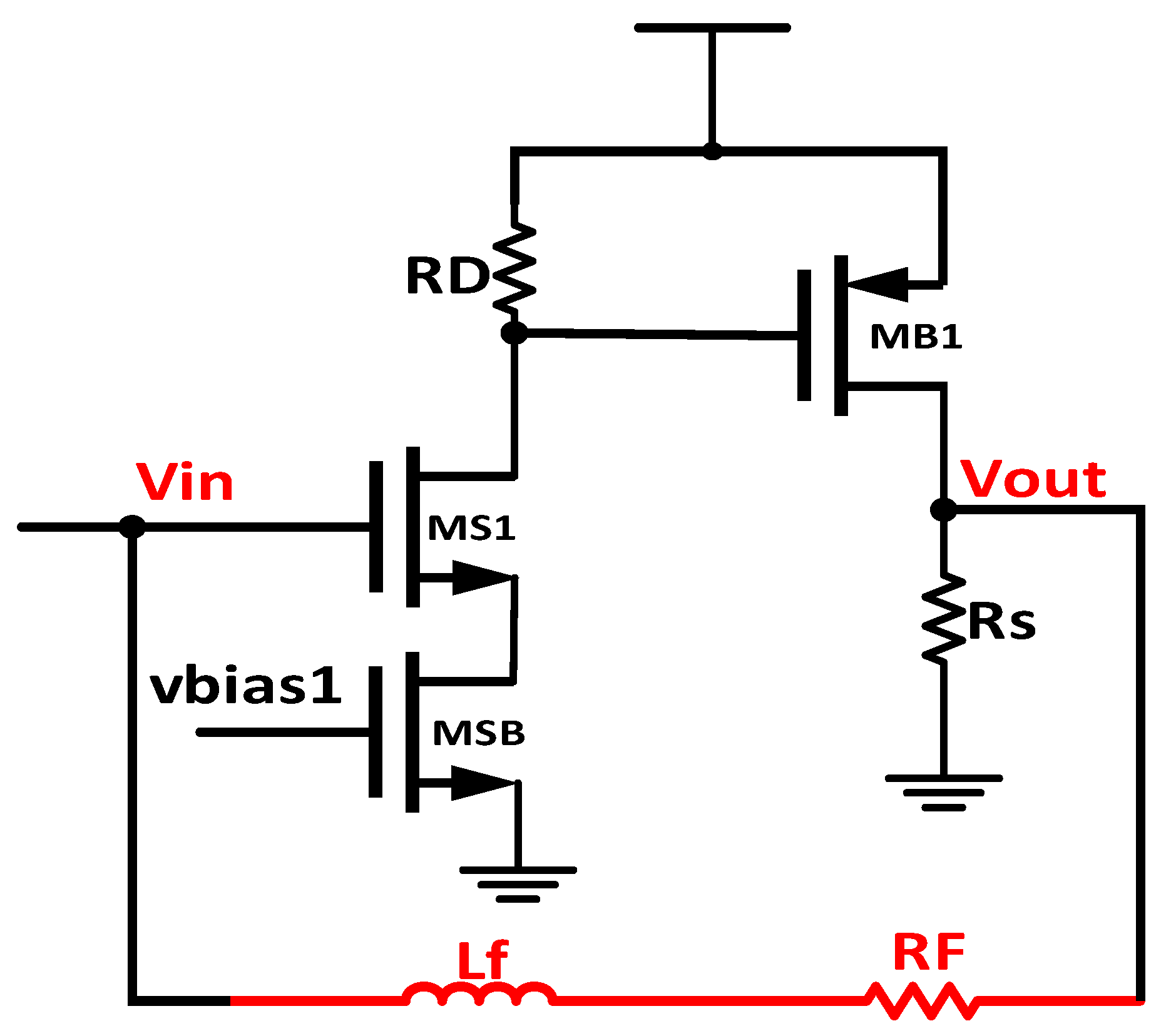
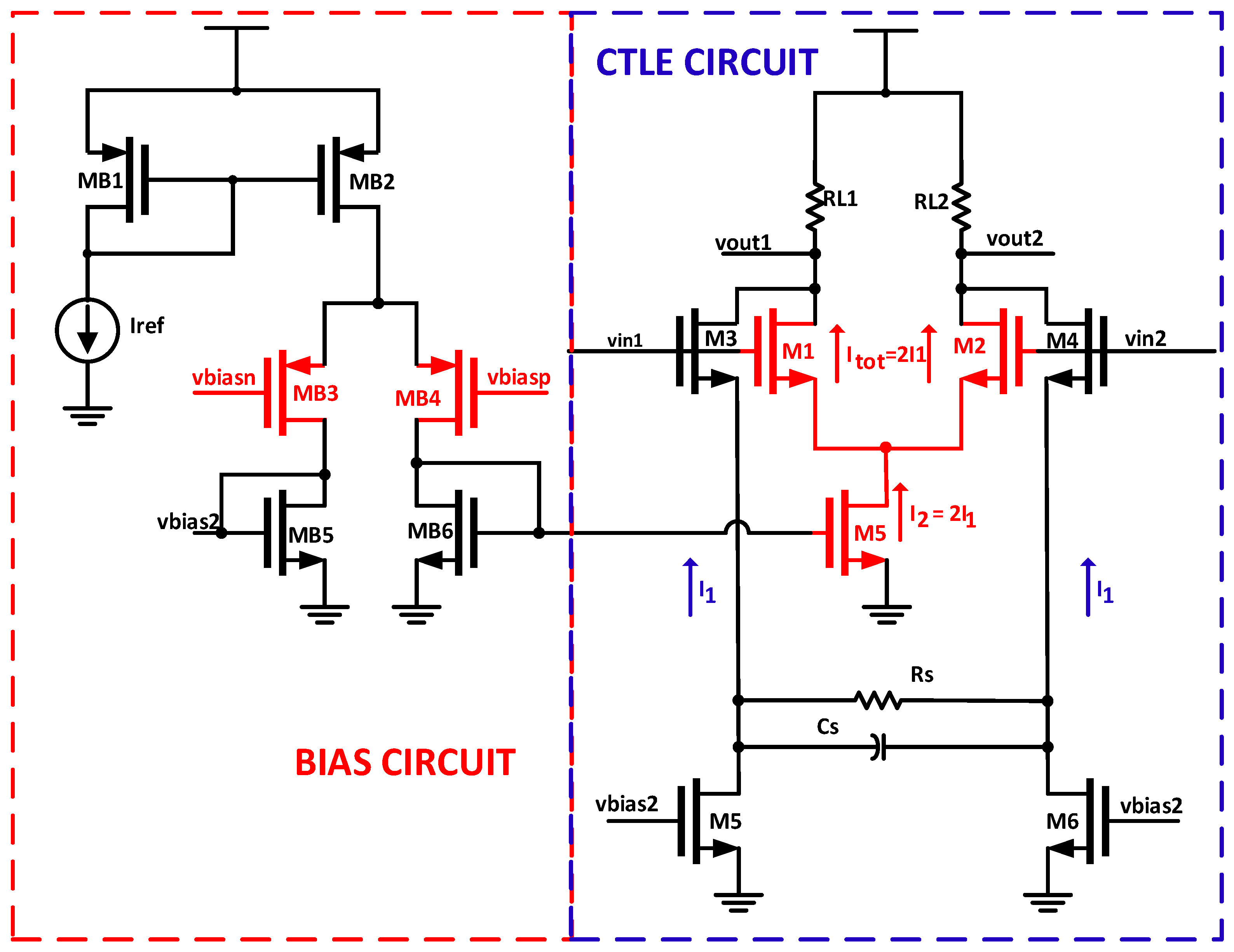
2.2. Proposed Continous-Time Linear Equalizer
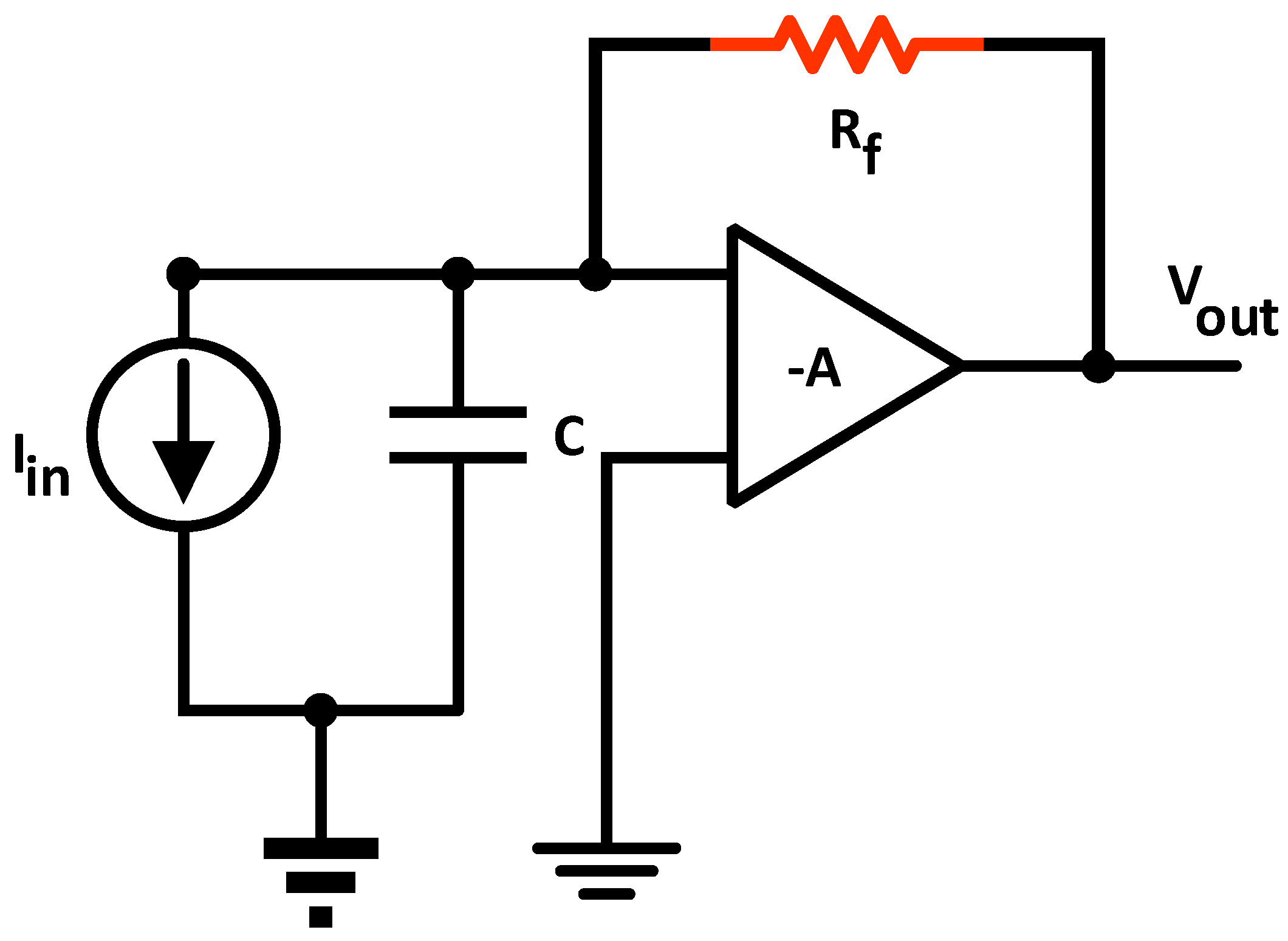
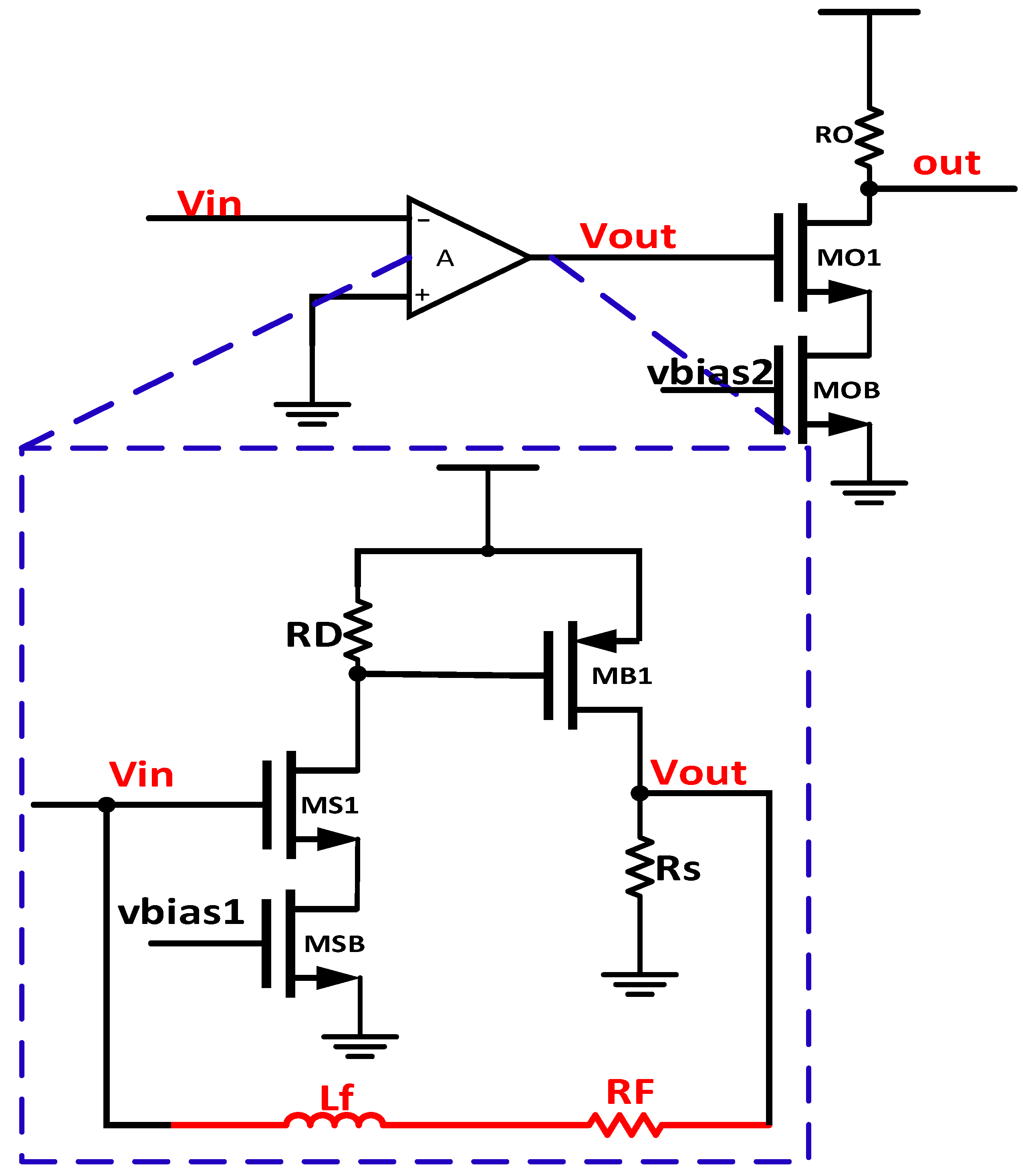
Figure 4 presents a schematic of the proposed CTLE comprising two differential pairs, M1 with M2 and M3 with M4. The differential pair comprising M3 and M4 is degenerated by the parallel resistor RS and the capacitor CS. M 5 ,   M 6 ,   and   M 7 are the current sinks and are controlled V b i a s 1 and V b i a s 2 .
The left-hand side of Figure 4 presents the bias circuit for the CTLE. The CTLE gain can be varied by adjusting the differential voltages of Vbiasn and Vbiasp. The differential voltages of Vbiasn and Vbiasp can be expressed as follows:
V b i a s n = V c m + / V a d j u s t
V b i a s p = V c m / + V a d j u s t
where Vcm is the common-mode voltage, and Vadjust is the adjusting voltage for varying the bias currents of the differential pairs of the CTLE. If Vbiasp > Vbiasn, the current I2 = 2I1 flows through M5, passes to M1 and M2, and the current I1 flowing through M6 and M7 passes to M3 and M4, as presented in Figure 4. The output current at nodes Vout1 and Vout2 is Itot = 2I1. Similarly, Vbiasp < Vbiasn; the output current at nodes Vout1 and Vout2 is Itot = 2I1. This design also boosts the DC gain at high frequency and slightly shifts the zero (ωz) and poles (ωp1 and ωp2). The zero ωz of the proposed CTLE is dependent on gm1 and gm3 and on RS and CS. The transfer function of the single-ended proposed CTLE is presented in Equation (8).
H   ( S ) = ( G M 1 + G M 3 ) R L 1 + ( G M 1 G M 3 ) R S 2   ×   1 + S ω z ( 1 + S ω p 1 ) ( 1 + S ω p 2 )
where ω z = 1 R s C s , ω p 1 = 1 + ( G M 1 G M 3 ) R s 2 R s C s , and ω p 2 = 1 R L C L are the zero and poles of the proposed CTLE.
The maximum boost gain at higher frequencies and the DC gain are determined using Equations (8) and (9).
ω p 1 ω z = 1 + ( G M 1 G M 3 ) R s
DC   gain = ( g m 1   × g m 3 ) R L 1 1 + ( G M 1 G M 3 ) R s 2
The Bode plot of the single-ended proposed CTLE with zeroes ωZ and ωZ1 that shift due to variations in the DC gain is presented in Figure 5.

2.3. TIA

A trade-off exists between the suitability of the DC operating point and performance at low frequency in this conventional gm transimpedance structure. The bandwidth fw and transimpedance gm in TIAs are decoupled. High-feedback resistance is necessary for good noise performance. Figure 6 presents a schematic of a TIA topology with a feedback resistor Rf. The input impedance is extended by a factor of A + 1, where A is the amplifier gain, and the transimpedance is approximately Rf [1,14,15].
For a fixed-bandwidth amplifier, the equivalent transfer function T(s) is as shown in Equation (10):
T ( S ) = V o u t I in = A 1 + A R f 1 + R f C 1 + A = A 1 + A R f
To achieve the desired DC operating point, transistor size ( W / L ) must be increased. However, bandwidth decreases, and large parasitic capacitances occur at the output nodes [15,17]. To overcome this problem, the SF state is introduced along with a shunt feedback resistor in the TIA as preferred in [14]. To increase the frequency bandwidth, a differential out-phase circuit is included in the TIA as shown in Figure 7.
A two-input differential TIA with resistor feedback along the inductor in series is implemented. The TIA can facilitate data transfer at all speeds tolerated by the interface. The architecture has three parts that each corresponds to a stage. The first part is a shunted feedback resistor, the second part is a simple buffer, and the third part is an entirely differential output phase. A single-ended schematic is presented in Figure 7 [14,17]. Specifically, the shunt feedback resistor in the first stage converts a current to a voltage. MS1 and RD are simple common sources, whereas MSB is the tail current. The second-stage MB1 acts as a buffer and inverter with two SFs enabling isolation between the input and output of the amplifier. The third stage, MO1, is the output phase, which increases the phase and increases the amplifier gain in which MoB is the tail current.
Figure 8 shows a single-ended TIA circuit with a common source stage and SF. The SF isolates RD from the loading effect of both Rf and Lf. The output impedance of the SF is less than the resistor feedback [17,20,21].
The open-loop gain of the amplifier is as follows:
T ( S ) = A 1 +   A G Ms R D 1 +   G Ms R D 1 Z
where Z is the impedance, which is the total resistance to current flow in a circuit containing both resistance Rf and inductor reactance XL. Z is defined as R f 2 + X L 2 .
The input and output impedances of the resistor feedback at low frequencies are as follows.
R Zin = Z   1 +   G Ms R D
R Zout = 1 G M B ( 1 + G MS R D )
The inductor and resistor in series, gives second order frequency 3 dB bandwidth as follows.
ω 3 d B = 2 ( 1 + A ) R D

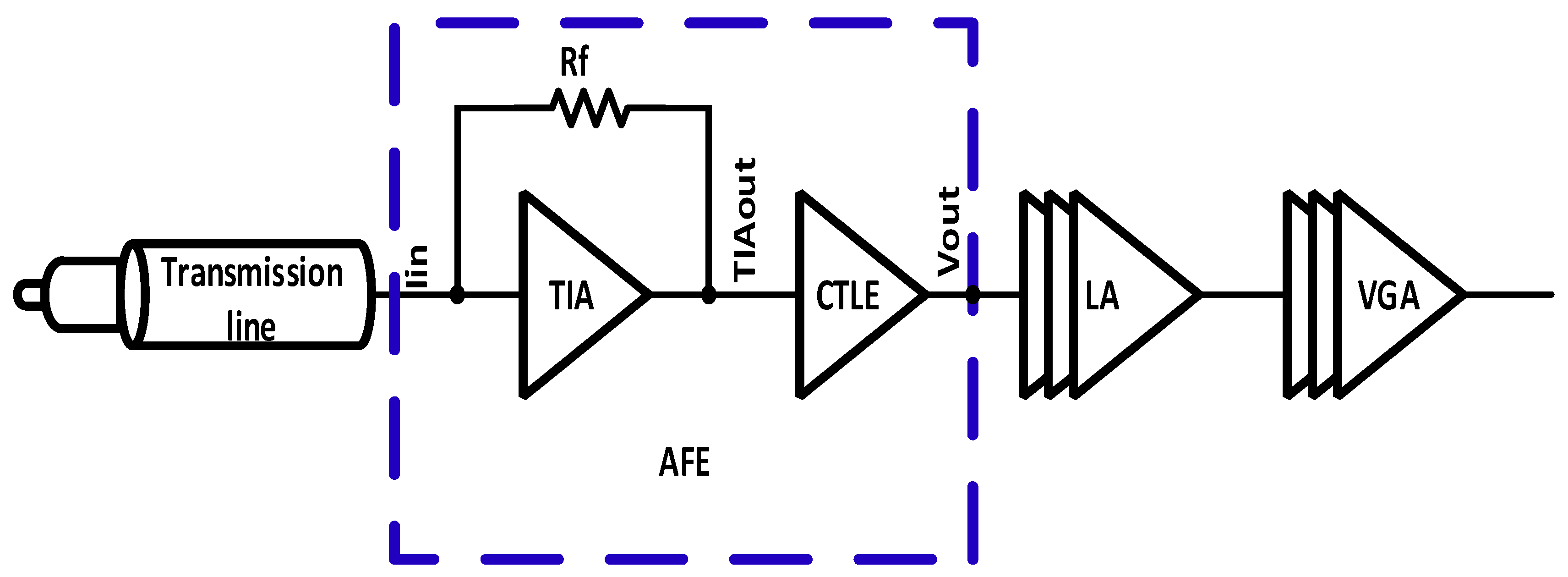
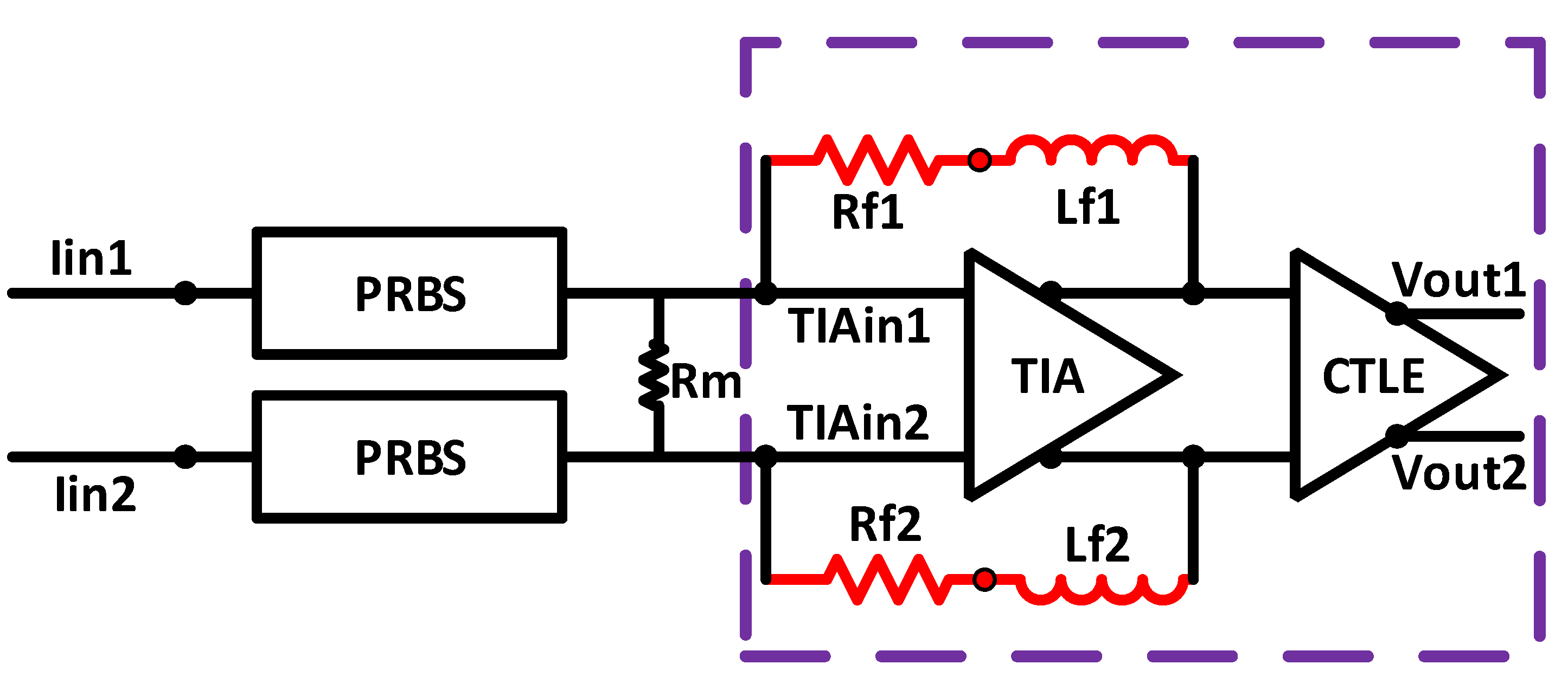
2.4. Reciever AFE Architecture
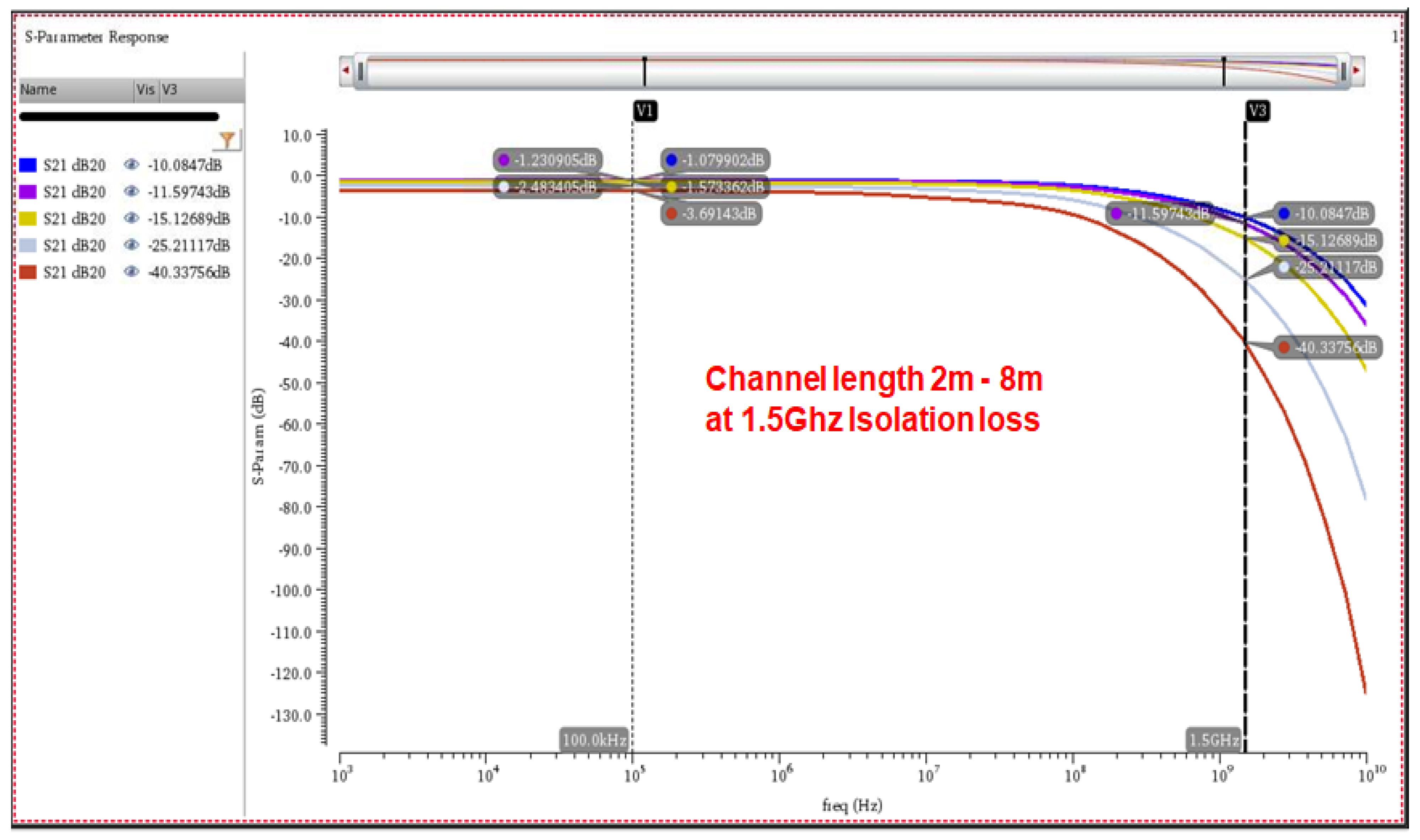
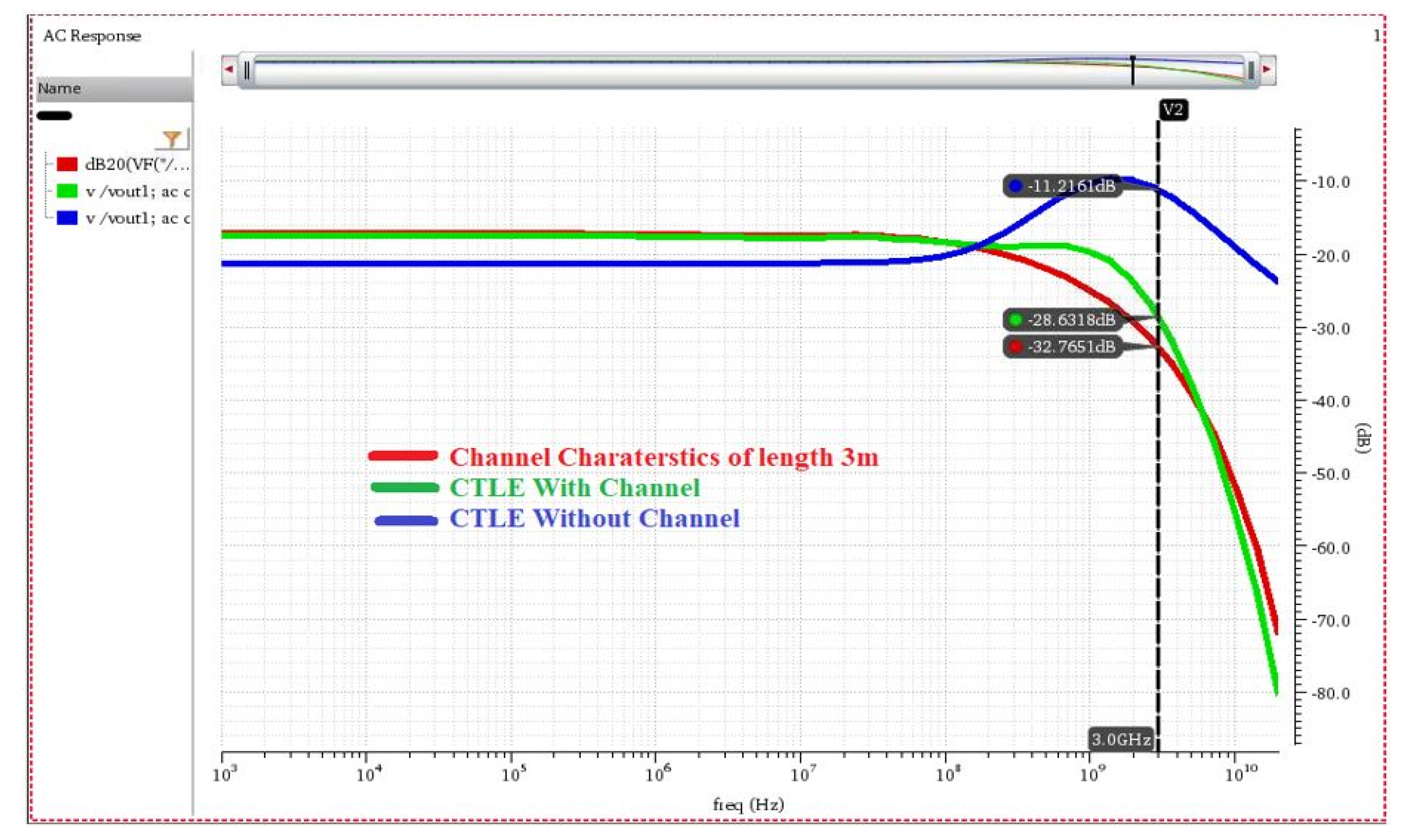
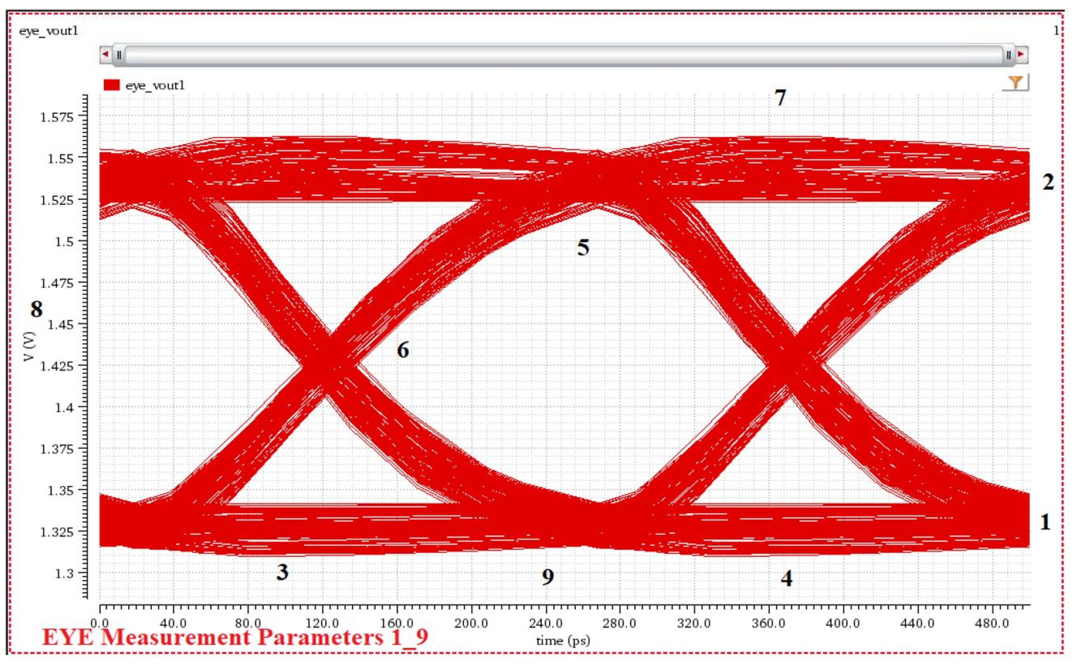
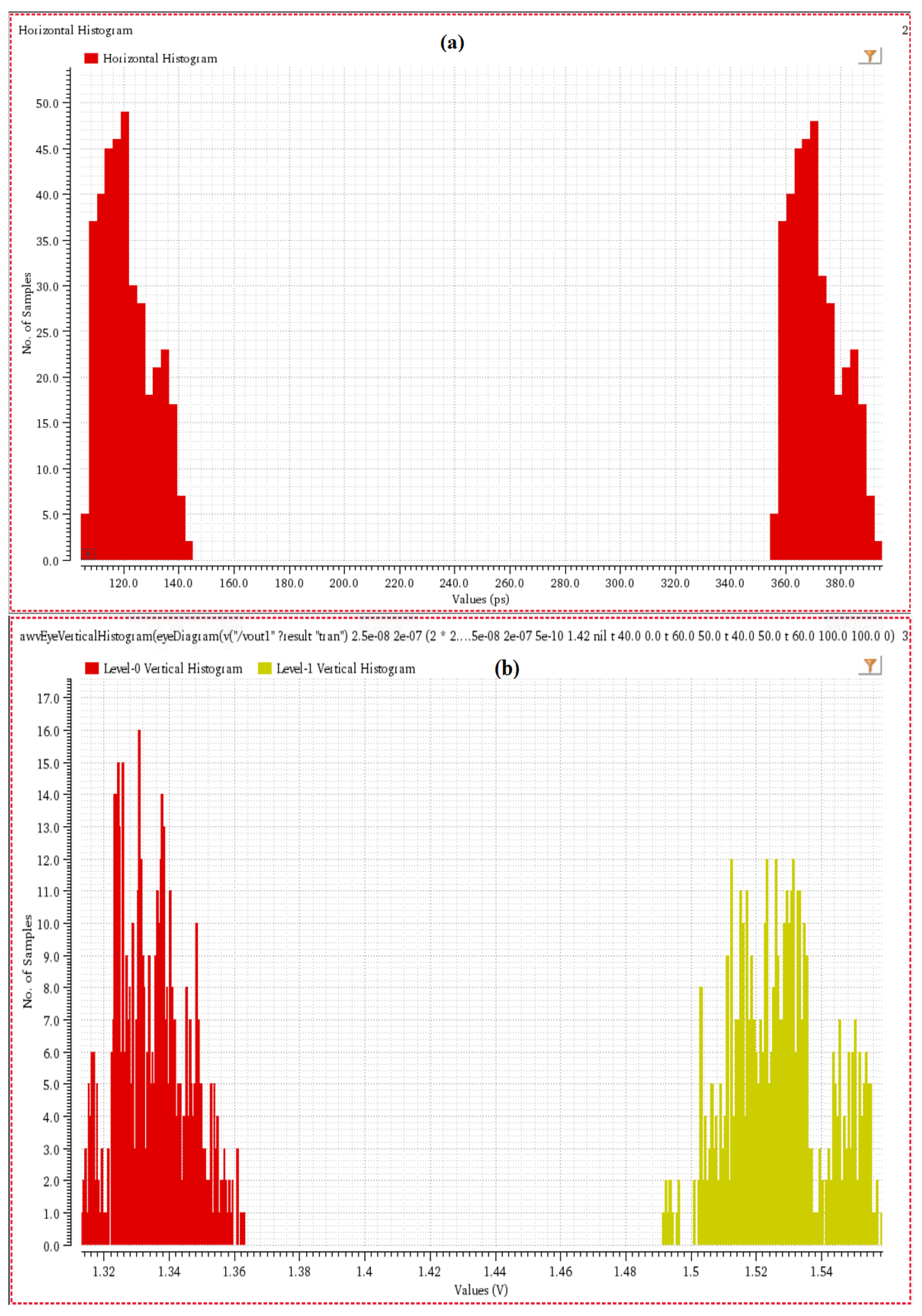
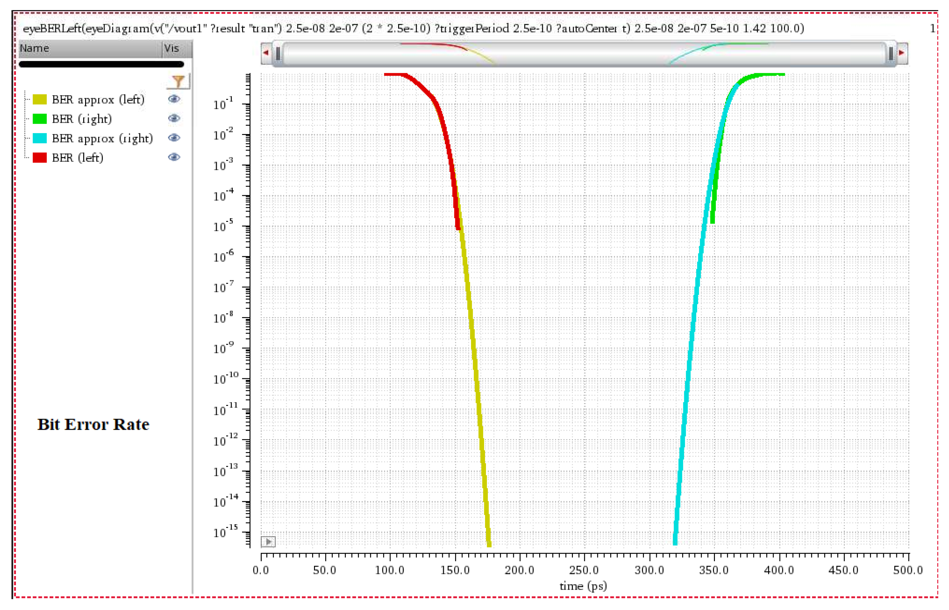
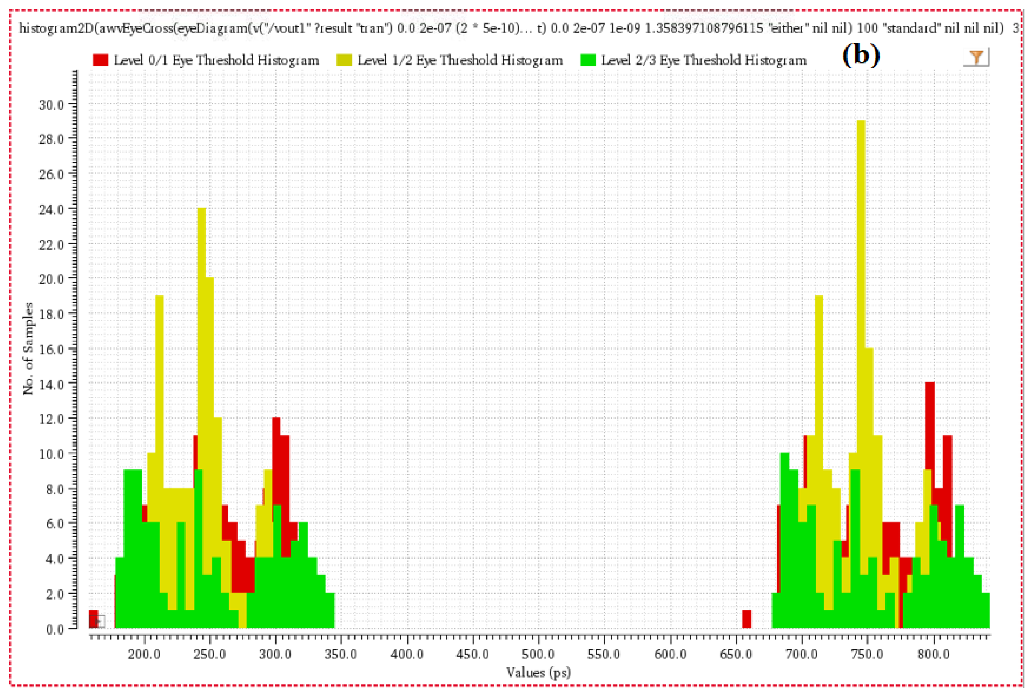
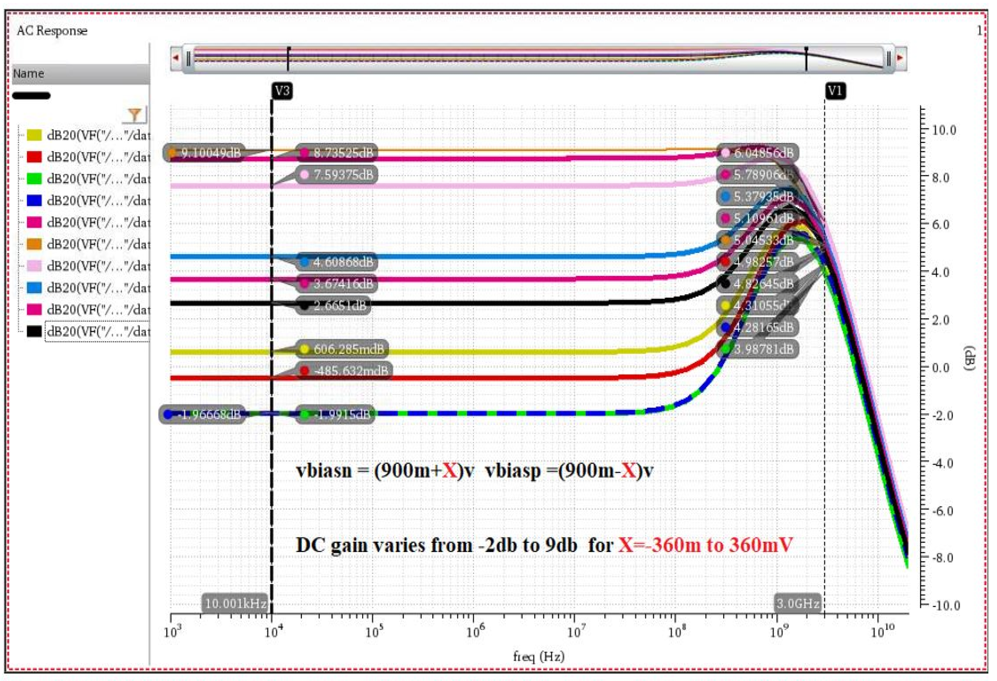
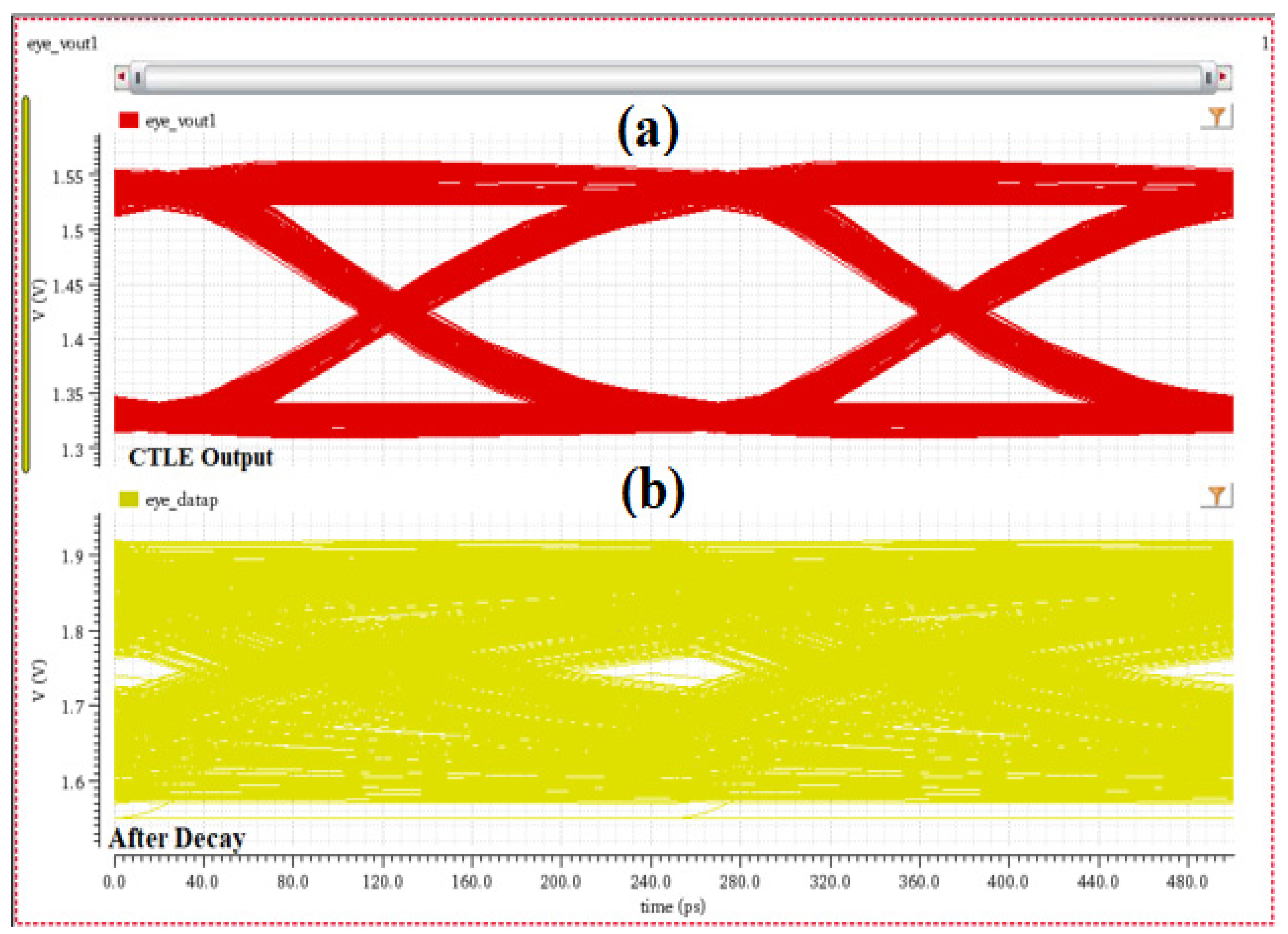
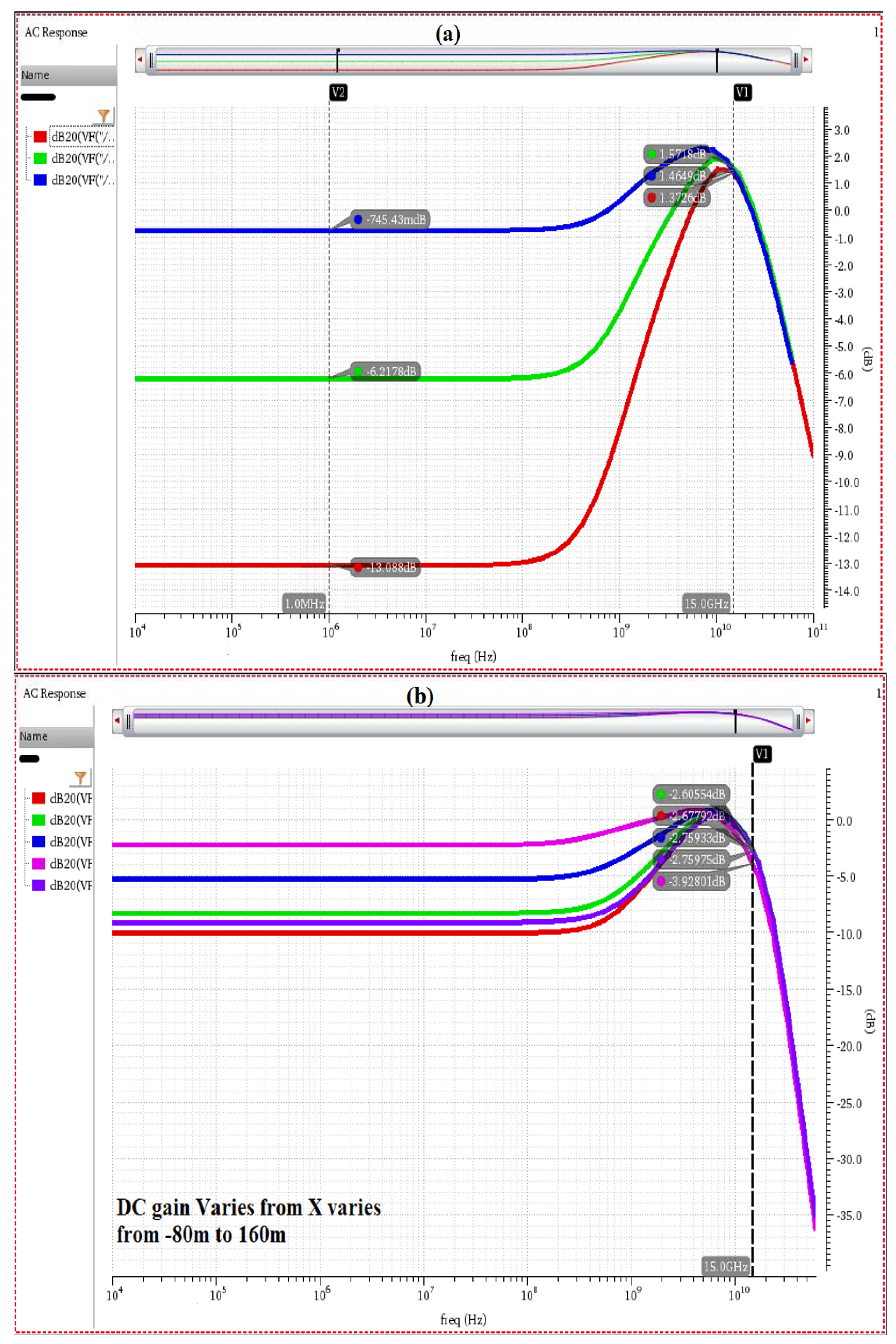
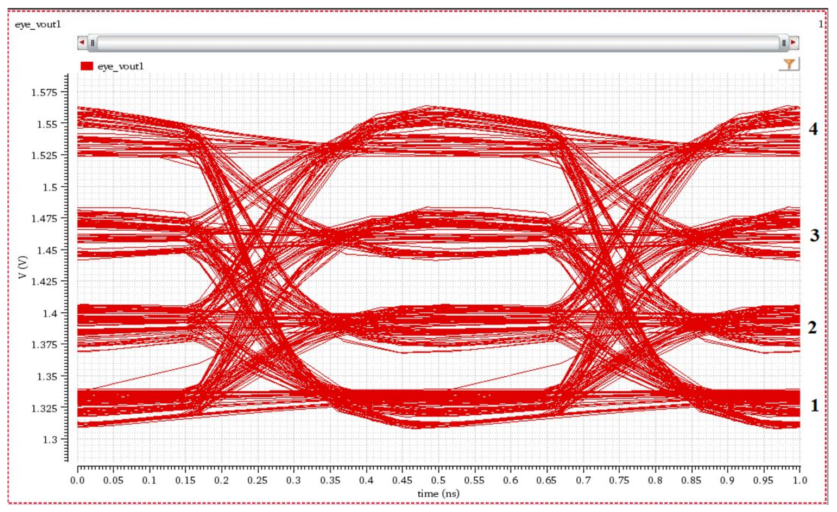
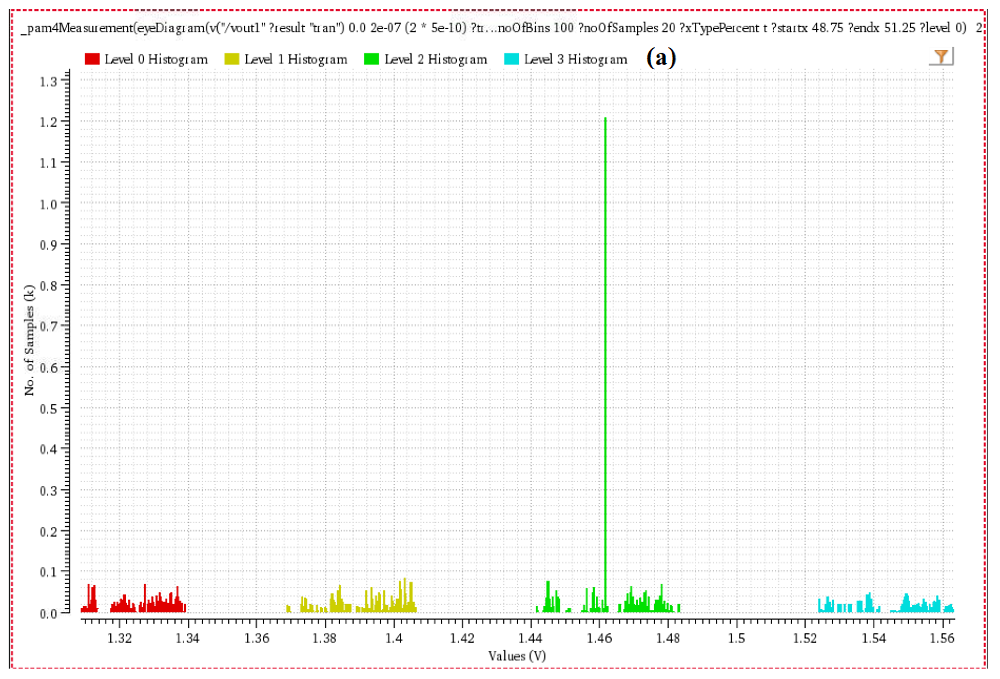
The AFE architecture presented in Figure 9 includes a differential Rm (100 Ω) termination, a two-stage CTLE and TIA, and a feedback resistor (Rf) and inductance reactance (Lf). The 100 Ω resistor was adopted to match the differential input of the circuit with that of the equipment. The AFE topology along the gm TIA with the CTLE compensates for the channel loss at a 15 GHz Nyquist frequency and adjusts the output amplitude without bandwidth deterioration [1,4,7]. The transfer function of the AFE circuit is as follows:
A v , D C = g m R D 1 +   g m R s 1   g m T I A , R F 1 + g m T I A , R D
A v , A C = A v , D C ( 1 + S ω z 1 ) ( 1 + S ω z 2 ) ( 1 + S ω p 1 ) ( 1 + S ω p 2 ) ( ( S ω n ) 2 + 2 § s ω n + 1 )
where ω z 1 = 1 R s C s ,   ω p 1   = 1 + G M R s 2 R s C s ,   ω n = 1 +   g m T I A , R D ( C L 2 L f ) , ω p 2 = 1 +   g m T I A , R D ( C L 2 L f R f ) ,   ω z 2 = 2 § w n , § = C L R D + g m T I A , L f 1 + g m T I A , R D / ( C L 2 L f ) 2 ( 1 + g m T I A , R D ) , CL2 is the capacitance load, Lf is the inductance reactance, Rf is the feedback resistance, and RD is the load resistance. The transfer function comprises one dominant pole ωp2 and two high-frequency poles ωn and ωp1. To increase the gain, Rf should be larger. However, the RC constant can be increased by simply increasing Rf, unexpectedly decreasing the bandwidth [22,23]. Thus, inductance reactance is used to increase bandwidth without changing the pole ωp2.

3. Results

The proposed AFE cascading TIA and CTLE was designed and simulated in a 180 nm complementary metal–oxide–semiconductor (CMOS) process. The performance of the CTLE, TIA, and the resulting eye diagram was simulated with Virtuoso 6.1.8–64 b software.
A high-frequency through-silicon scalable electrical model using a field solver was used as a transmission line (channel) [24,25]. Figure 10 reveals that the simulated channel can achieve 10 dB decay isolation loss at a 1.5 GHz Nyquist frequency for different cable lengths (2–8 m).
Figure 11 reveals that the simulated CTLE can achieve a DC gain of −2 to 9 dB at a 3 GHz Nyquist frequency by tuning bias voltage Vbiasn and Vbiasp and adjusting the voltage Vadjust (represented by X in Figure 11) from +360 to −360 mV for a channel length of 3 m. Figure 12 presents the characteristics of CTLE with and without a 3 m channel at a 3 GHz Nyquist frequency.
Figure 13 presents the simulated single-ended 6 Gb/s NRZ eye diagrams with the two different lossy channels. Figure 13b reveals that output eye is closed at the decay stage in which the CTLE is disabled. By contrast, Figure 13a reveals that the 6 Gb/s NRZ eyes are open if the CTLE is enabled.
In this case, the input signal was a simulated NRZ pseudorandom bit sequence 231 − 1 with a peak-to-peak amplitude of 189.914 mV; the root-mean square jitter was 8.86 picosecond. An input and output impedance of 50 Ω and a 50 pf capacitor were used in this case. Figure 14 presents all measured parameters of the simulated eye diagram.
Figure 15 presents the simulated histogram plots used to calculate the eye width and height. Figure 15a presents a horizontal histogram used to measure the eye width at each time point and to sum up the number of traces across vertical bins. Figure 15b is a vertical histogram of eye height measurements for every amplitude point; these points were summed across the time axis.
Simulated BER bathtub curves for NRZ input data rates of 6 Gb/s are presented in Figure 16. The BER variations for different positions of the sampling point for both time delay and the voltage–power relationship are presented in Figure 16. In this case, BER(t) was 0.16 × 10⁻¹². Table 1 summarizes the key performance metrics of the proposed CTLE and other recently published CTLEs. The proposed CTLE achieved a peaking frequency with constant current for tuning its equalization competence.
Figure 17 presents the simulated frequency response of the AFE cascading the CTLE and the TIA. Subsequently, the bandwidth must recover from 6 GHz (approximately 18/3 GHz) to 15 GHz; thus, the equalizer is tuned to its maximum peaking. To reach this required bandwidth, the TIA is designed to boost the equalizer by introducing a feedback resistor Rs and inductor Lf. The frequency response for AFE reached 15 GHz at various bias voltages (−80, 0, and 80 mV) with 12 dB channel losses at a 15 GHz Nyquist frequency with a 3 m channel (Figure 17a). Similarly, Figure 17b reveals that the DC gain varies as Vadjust varied from −80 to 160 mV at a 15 GHz Nyquist frequency.
Figure 18 reveals that the simulated single-ended 30 Gb/s PAM4 eyes are open for 12 dB of channel loss at a 15 GHz Nyquist frequency. The PAM4 eyes parameters are indicated as (1)–(4) in the figure. The simulated 0-leVel (1), 1-leVel (2), 2-leVel (3), and 3-leVel (4) voltages were 1.325, 1.392, 1.463, and 1.544 V, respectively. The eye width of levels 0/1, 1/2, and 2/3 were all 375 ps. Figure 19a presents the width of a simulated level-4 eye using the histograms for the other levels. Similarly, Figure 19b presents the bit periods for level 0/1, 1/2, and 2/3 through threshold histograms.
Table 2 presents the key performance metrics of the proposed AFE and other recently proposed AFEs.

4. Conclusions

The simulated two-stage differential input pair CTLE can successfully compensate for 16 dB of channel loss at a 3 GHz Nyquist frequency and can open the closed-eye 6 Gb/s NRZ signal with an energy efficiency of 8 pJ/bit and a BER of 0.16 × 10⁻¹² from a 231 − 1 pseudorandom binary sequence input. The TIA topology can achieve higher bandwidth, ameliorating the trade-off between bandwidth and DC gain. The AFE compensated for 12 dB of channel loss at a 15 GHz Nyquist frequency and opened closed eyes for a 30 Gb/s PAM4 signal from a pseudorandom binary sequence input; it consumed 27 mW of power from a 1.8 V supply.

Author Contributions

P.V.S.C.N. contributed to the schematic design, simulation in software, and simulation results of the proposed circuits, as well as writing the paper. C.-W.L. contributed to advice on the design process, simulation, and editing of this paper. All authors have read and agreed to the published version of the manuscript.

Funding

This research received no external funding.

Acknowledgments

The authors would like to acknowledge the Chip Implementation Center (CIC), Taiwan, for its EDA tools, facility, and technology support.

Conflicts of Interest

The authors declare no conflict of interest.

References

  1. Kimura, H.; Aziz, P.; Jing, P.; Sinha, A.; Narayan, R.; Gao, H.; Jing, P.; Hom, G.; Liang, A.; Zhang, E.; et al. A 28 Gb/s 560 mW Multi-Standard SerDes with Single-Stage Analog Front-End and 14-Tap Decision Feedback Equalizer in 28 nm CMOS. In Proceedings of the 2014 IEEE International Solid-State Circuits Conference Digest of Technical Papers (ISSCC), San Francisco, CA, USA, 9–13 February 2014; Volume 49, pp. 3091–3103. [Google Scholar]
  2. Takemoto, T.; Yamashita, H.; Yazaki, T.; Chujo, N.; Lee, Y.; Matsuoka, Y. A 4 25-to-28 Gb/s 4.9 mW/Gb/s 9.7 dBm high-sensitivity optical receiver based on 65 nm CMOS for board-to-board interconnects. In Proceedings of the 2013 IEEE International Solid-State Circuits Conference Digest of Technical Papers, San Francisco, CA, USA, 17–21 February 2013; pp. 118–119. [Google Scholar]
  3. Kim, M.; Bae, J.; Ha, U.; Yoo, H.J. A 24-mW 28-Gb/s wireline receiver with low-frequency equalizing CTLE and 2-tap speculative DFE. In Proceedings of the IEEE International Symposium on Circuits and Systems (ISCAS), Lisbon, Portugal, 24–27 May 2015; pp. 1610–1613. [Google Scholar]
  4. Parikh, S.; Kao, T.; Hidaka, Y.; Jiang, J.; Toda, A.; Mcleod, S.; Walker, W.; Koyanagi, Y.; Shibuya, T.; Yamada, J. A 32 Gb/s wireline receiver with a low-frequency equalizer, CTLE and 2-Tap DFE in 28 nm CMOS. In Proceedings of the 2013 IEEE International Solid-State Circuits Conference Digest of Technical Papers, San Francisco, CA, USA, 17–21 February 2013; pp. 28–29. [Google Scholar]
  5. Kim, J.; Buckwalter, J.F. A 40-Gb/s optical transceiver front-end in 45 nm SOI CMOS. IEEE J. Solid-State Circuits 2012, 47, 615–626. [Google Scholar] [CrossRef]
  6. Säckinger, E. Broadband Circuits for Optical Fiber Communication; Wiley: New York, NY, USA, 2005. [Google Scholar]
  7. Lee, J. A 20-Gb/s Adaptive Equalizer in 0.13-um CMOS Technology. IEEE J. Solid-State Circuits 2006, 41, 2058–2066. [Google Scholar] [CrossRef]
  8. Zheng, K.; Frans, Y.; Chang, K.; Murmann, B. A 56 Gb/s 6 mW 300 um2 inverter-based CTLE for short-reach PAM2 applications in 16 nm CMOS. In Proceedings of the 2018 IEEE Custom Integrated Circuits Conference (CICC), San Diego, CA, USA, 8–11 April 2018; pp. 1–4. [Google Scholar]
  9. Hyun, C.; Ko, H.; Chae, J.; Park, H.; Kim, S. A 20 Gb/s Dual-Mode PAM4/NRZ Single-Ended Transmitter with RLM Compensation. In Proceedings of the 2019 IEEE International Symposium on Circuits and Systems (ISCAS), Sapporo, Japan, 26–29 May 2019; pp. 1–4. [Google Scholar]
  10. Roshan-Zamir, A.; Elhadidy, O.; Yang, H.; Palermo, S. A Reconfigurable 16/32 Gb/s Dual-Mode NRZ/PAM4 SerDes in 65-nm CMOS. IEEE J. Solid-State Circuits 2017, 52, 2430–2447. [Google Scholar] [CrossRef]
  11. Komatsu, Y.; Shinmyo, A.; Kato, S.; Funabashi, M.; Hatooka, K.; Fujita, M.; Tanaka, K.; Yamasaki, A.; Fukuda, K. A 0.25–27-Gb/s PAM4/NRZ Transceiver with Adaptive Power CDR and Jitter Analysis. IEEE J. Solid-State Circuits 2019, 54, 2802–2811. [Google Scholar] [CrossRef]
  12. Lee, J.; Chiang, P.; Peng, P.; Chen, L.; Weng, C. Design of 56 Gb/s NRZ and PAM4 SerDes Transceivers in CMOS Technologies. IEEE J. Solid-State Circuits 2015, 50, 2061–2073. [Google Scholar] [CrossRef]
  13. Lee, J.; Chen, M.; Wang, H. Design and Comparison of Three 20-Gb/s Backplane Transceivers for Duobinary, PAM4, and NRZ Data. IEEE J. Solid-State Circuits 2008, 43, 2120–2133. [Google Scholar] [CrossRef] [Green Version]
  14. Razavi, B. The Transimpedance Amplifier [A Circuit for All Seasons]. IEEE Solid-State Circuits Mag. 2019, 11, 10–97. [Google Scholar] [CrossRef]
  15. Wang, J.; Pan, Q.; Qin, Y.; Chen, X.; Hu, S.; Bai, R. A fully-integrated 25 Gb/s low-noise TIA+CDR optical receiver designed in 40nm-CMOS. In Proceedings of the IEEE Transactions on Circuits and Systems II: Express Briefs, Tainan, Taiwan, 27 June 2019; pp. 67–68. [Google Scholar]
  16. Lee, J.; Lee, K.; Kim, H.; Kim, B.; Park, K.; Jeong, D. A 0.1-pJ/b/dB 1.62-to-10.8-Gb/s Video Interface Receiver with Jointly Adaptive CTLE and DFE Using Biased Data-Level Reference. IEEE J. Solid-State Circuits 2020, 55, 2186–2195. [Google Scholar] [CrossRef]
  17. Lin, Y.T.; Chen, H.C.; Wang, T.; Lin, Y.S.; Lu, S.S. S. 3–10-GHz ultra-wideband low-noise amplifier utilizing miller effect and inductive shunt-shunt feedback technique. IEEE Trans. Microw. Theory Techn. 2007, 55, 1832–1843. [Google Scholar] [CrossRef]
  18. Choi, J.-S.; Hwang, M.-S.; Jeong, D.-K. A 0.18-um CMOS 3.5-Gb/s continuous-time adaptive cable equalizer using enhanced low-frequency gain control method. IEEE J. Solid-State Circuits 2004, 39, 419–425. [Google Scholar] [CrossRef]
  19. Li, D.; Minoia, G.; Repossi, M.; Baldi, D.; Temporiti, E.; Mazzanti, A. A low-noise design technique for high-speed CMOS optical receivers. IEEE J. Solid-State Circuits 2014, 49, 1437–1447. [Google Scholar] [CrossRef]
  20. Li, C.; Palermo, S. A low-power 26-GHz transformer-based regulated cascode SiGe BiCMOS transimpedance amplifier. IEEE J. Solid-State Circuits 2013, 48, 1264–1275. [Google Scholar] [CrossRef]
  21. Galal, S.; Razavi, B. 10-Gb/s limiting amplifier and laser/modulator driver in 0.18-m CMOS technology. IEEE J. Solid-State Circuits 2003, 38, 2138–2146. [Google Scholar] [CrossRef]
  22. Hsiao, J.; Jhou, D.; Lee, T. A 10-Gb/s equalizer with digital adaptation. In Proceedings of the 2017 International SoC Design Conference (ISOCC), Seoul, Korea, 5–8 November 2017; pp. 38–39. [Google Scholar]
  23. Chen, K.-Y.; Chen, W.-Y.; Liu, S.-I. A 0.035-pJ/bit/dB 20-Gb/s adaptive linear equalizer with an adaptation time of 2.68 μs. IEEE Trans. Circuits Syst. II Exp. Briefs 2017, 64, 645–649. [Google Scholar] [CrossRef]
  24. Raj, M.; Monge, M.; Emami, A. Amodelingg and nonlinear equalization technique for a 20 Gb/s 0.77 pJ/b VCSEL transmitter in 32 nm SOI CMOS. IEEE J. Solid-State Circuits 2016, 51, 1734–1743. [Google Scholar] [CrossRef]
  25. Kim, J.; Pak, J.S.; Cho, J.; Song, E.; Cho, J.; Kim, H.; Song, T.; Lee, J.; Lee, H.; Park, K.; et al. High-Frequency Scalable Electrical Model and Analysis of a Through Silicon Via (TSV). IEEE Trans. Compon. Packag. Manuf. Technol. 2011, 1, 181–195. [Google Scholar] [CrossRef]
Figure 1. Block Diagram of a Receiver with an AFE.
Electronics 11 01546 g001
Figure 2. Schematic of Conventional CTLE.
Electronics 11 01546 g002
Figure 3. Single-ended Bode Plot of the CTLE.
Electronics 11 01546 g003
Figure 4. Schematic of Proposed CTLE.
Electronics 11 01546 g004
Figure 5. Single-ended Bode Plot of the Proposed CTLE.
Electronics 11 01546 g005
Figure 6. Simple TIA Topology with feedback resistor Rf.
Electronics 11 01546 g006
Figure 7. Schematic of Single-ended TIA.
Electronics 11 01546 g007
Figure 8. Single end of the TIA.
Electronics 11 01546 g008
Figure 9. Receiver AFE Architecture.
Electronics 11 01546 g009
Figure 10. Variations in Channel Characteristics for Lengths of 2 m–8 m at 1.5 GHz.
Electronics 11 01546 g010
Figure 11. Simulated Frequency Response for the CTLE.
Electronics 11 01546 g011
Figure 12. Simulated AC response of the CTLE with and without the Channel.
Electronics 11 01546 g012
Figure 13. Simulated Output Eyes (a) with CTLE Enabled and (b) with CTLE Disabled.
Electronics 11 01546 g013
Figure 14. Simulated Eye Diagram. (1) 0 level at 1.33 V; (2) 1 level at 1.52 V; (3) and (4) rise and fall time of 102.2 and 95.1151 ps, respectively; (5) and (6) eye height and width of 118.882 mV and 196.79 ps, respectively.
Electronics 11 01546 g014
Figure 15. (a) Horizontal Histogram and (b) Vertical Histogram of eye diagrams for the 0 and 1 levels.
Electronics 11 01546 g015
Figure 16. Simulated BER(t) bathtub curves for the 6 Gb/s NRZ signal.
Electronics 11 01546 g016
Figure 17. Simulated frequency response for the AFE. (a) 12 dB by tuning Vbias from −80, 0, and 80 mV and (b) from −80 to 160 mV.
Electronics 11 01546 g017
Figure 18. Eye diagram AFE for PAM4 signal.
Electronics 11 01546 g018
Figure 19. (a) Histogram of the eye diagram reveals eye widths for levels 0, 1, 2, and 3. (b) Threshold histogram of the eye diagram reveals the bit period of levels 0/1, 1/2, and 2/3.
Electronics 11 01546 g019aElectronics 11 01546 g019b
Table 1. Performance comparison.
Equalization[9][10][12][13]This Work
Data rate (Gbps)101616205–15
Channel loss (dB)NyquistNA27.620.51216
Eye   width @ BER   <   10 12 0.620.180.16NA0.16
Supply (V)11.21.21.51.8
Power (mW)72173.17173.1710014
Technology65 nm65 nm65 nm90 nm180 nm
Table 2. Performance comparison.
Reference[1][4][15][23]This Work
Technology CMOS28 nm28 nm40 nm40 nm180 nm
Power supply1.5 V0.9 V1 V1.2 V1.8 V
Equalization14-tap CTLECTLE+DFECTLECTLECTLE
Data rate range (Gbps)1.25~28.5328~10205~30
Power (mW)5602401012.827
Channel loss (@GHz)34 dB@1437 dB@1617 dB@418 dB@1028 dB@15
Publisher’s Note: MDPI stays neutral with regard to jurisdictional claims in published maps and institutional affiliations.

