
A Thermally Stable Quasi-CMOS Bipolar Logic


Abstract
:1. Introduction
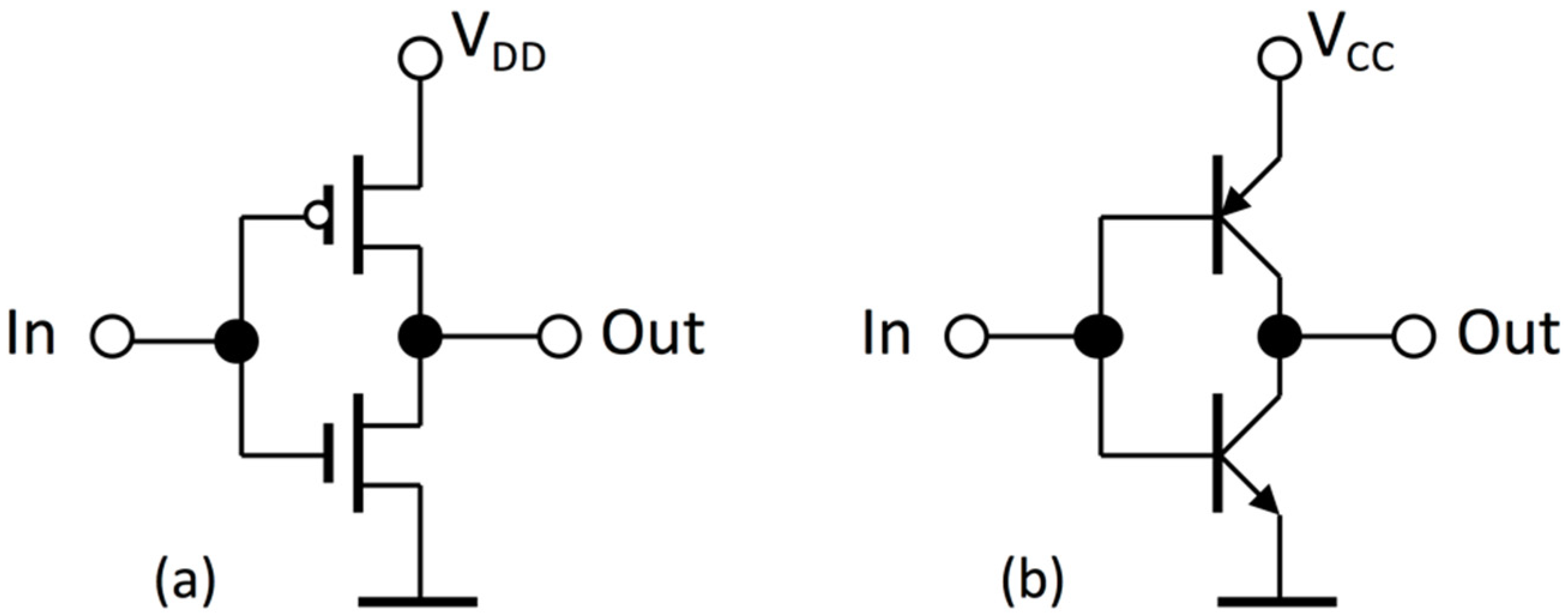
2. Thermal Stability of CBip Gates
3. CBip Gates and Circuits
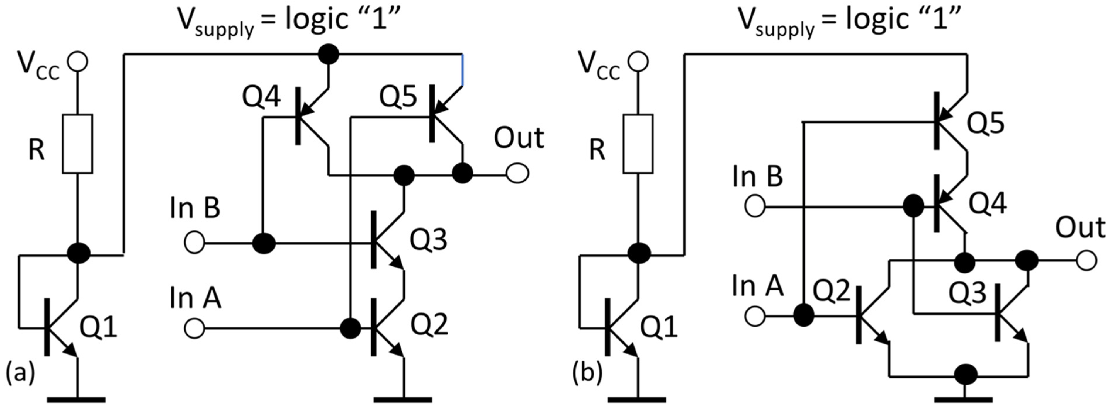
3.1. NAND and NOR Gates
3.2. AND and OR Gates
3.3. The Effects of Load
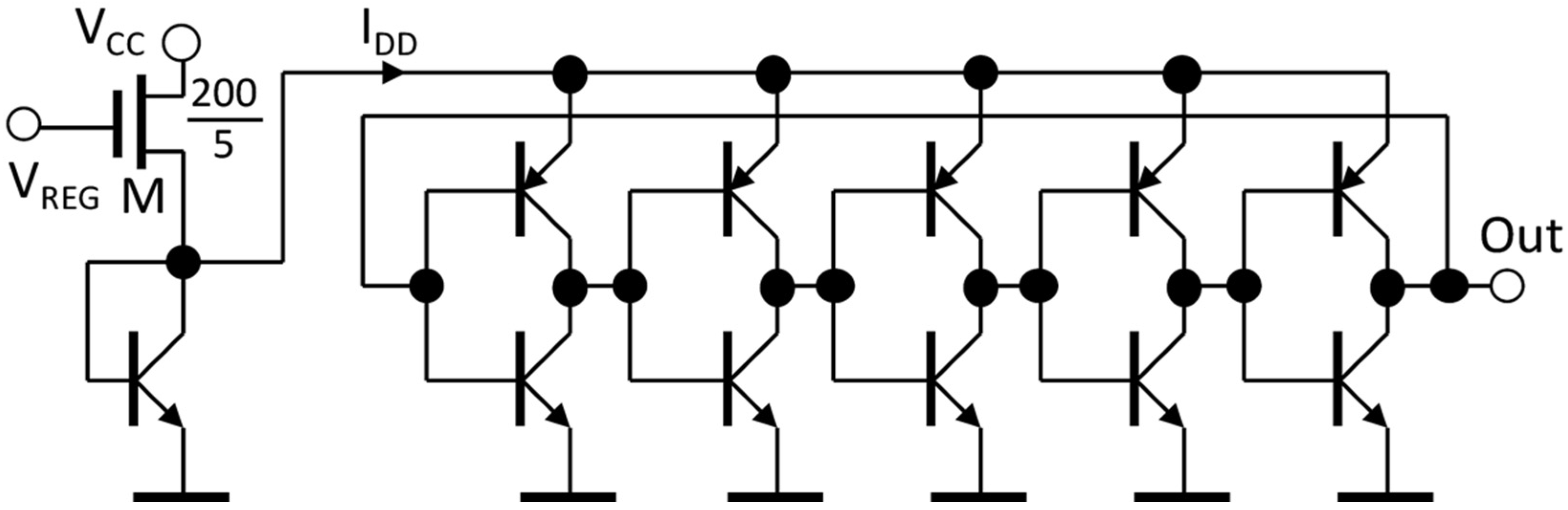
3.4. Two Examples
4. Discussion and Conclusions
Funding
Conflicts of Interest
Acronyms
| NPN | denotes bipolar transistor with emitter and collector made of n-type semiconductor and base of p-type semiconductor. |
| PNP | denotes bipolar transistor with emitter and collector made of p-type semiconductor and base of n-type semiconductor. |
| CMOS | Complementary Metal-Oxide-Semiconductor—logic gates that use complementary pairs of p-type and n-type MOS transistors. |
| TTL | Transistor–Transistor Logic—logic gates that use NPN bipolar transistors. |
| TTL-S | Transistor—Transistor Logic with Schottky diodes—logic gates that use NPN bipolar transistors with Schottky diodes in order to reduce the switching time of bipolar transistors. |
| ECL | Emitter-Coupled Logic: another kind of logic gates that uses bipolar transistors. |
| VLSI | Very Large-Scale Integration—technology enabling fabrication of complex integrated circuits, which combine millions of MOS transistors in a single semiconductor chip. |
| SOI | Silicon on Insulator—silicon layer located on top of silicon dioxide insulating layer. |
| SRAM | Static Random-Access Memory—semiconductor memory that preserves the content of memory cells as long as they are powered, no refreshing of the content necessary. |
| PD-SOI | Partially Depleted Silicon on Insulator—CMOS technology in which MOS devices are made in a relatively thick silicon layer located on top of silicon dioxide insulating layer. |
| FD-SOI | Fully Depleted Silicon on Insulator—CMOS technology in which MOS devices are made in a very thin silicon layer located on top of silicon dioxide insulating layer. |
| CBip | Logic gates discussed in this paper that use complementary pairs of bipolar NPN and PNP transistors, different from TTL, TTL-S or ECL gates. |
| NAND, NOR, AND, OR | Names of logic gates performing the respective logic functions. |
| RF | Radio Frequency—name often used for electronic circuits working in the microwave range of frequencies. |
Appendix A. Analysis of Thermal Stability of a CBip Inverter
Appendix B. Device Models
- Bipolar transistor models identical for NPN and PNP devices:MODEL QMODN NPN(is = 2e-19 bf = 10 br = 10 re = 20 rb = 20 var = 25 vaf = 25 ikf = 5.15e-4
- +ikr = 5.15e-4 cje = 6e-17 cjc = 6e-17 vjc = 1 vje = 1 tf = 4.2e-12 tr = 4.2e-12)
MODEL QMODP PNP(is = 2e-19 bf = 10 br = 10 re = 20 rb = 20 var = 25 vaf = 25 ikf = 5.15e-4- +ikr = 5.15e-4 cje = 6e-17 cjc = 6e-17 vjc = 1 vje = 1 tf = 4.2e-12 tr = 4.2e-12)
- Bipolar transistor models—NPN device with higher hFE than PNP device, used in simulations shown in Figure 9, Figure 10, Figure 19 and Figure 21:MODEL QMODN NPN(is = 5e-19 bf = 100 br = 100 re = 20 rb = 20 var = 25 vaf = 25 ikf = 5.15e-4
- +ikr = 5.15e-4 cje = 2e-18 cjc = 2e-18 vjc = 1 vje = 1 tf = 4.2e-12 tr = 4.2e-12)
MODEL QMODP PNP(is = 2e-19 bf = 10 br = 10 re = 20 rb = 20 var = 25 vaf = 25 ikf = 5.15e-4- +ikr = 5.15e-4 cje = 2e-18 cjc = 2e-18 vjc = 1 vje = 1 tf = 4.2e-12 tr = 4.2e-12)
- +version = 4.6.5 binunit = 1 paramchk = 1 mobmod = 0
- +capmod = 2 igcmod = 1 igbmod = 1 geomod = 1
- +diomod = 1 rdsmod = 0 rbodymod = 1 rgatemod = 1
- +permod = 1 acnqsmod = 0 trnqsmod = 0
- +tnom = 27 toxe = 1.05e-009 toxp = 8e-010 toxm = 1.05e-009
- +dtox = 2.5e-010 epsrox = 3.9 wint = 5e-009 lint = 2e-009
- +ll = 0 wl = 0 lln = 1 wln = 1
- +lw = 0 ww = 0 lwn = 1 wwn = 1
- +lwl = 0 wwl = 0 xpart = 0 toxref = 1.05e-009
- +xl = -9e-9
- +vth0 = 0.50308 k1 = 0.4 k2 = 0 k3 = 0
- +k3b = 0 w0 = 2.5e-006 dvt0 = 1 dvt1 = 2
- +dvt2 = 0 dvt0w = 0 dvt1w = 0 dvt2w = 0
- +dsub = 0.1 minv = 0.05 voffl = 0 dvtp0 = 1e-011
- +dvtp1 = 0.1 lpe0 = 0 lpeb = 0 xj = 7.2e-009
- +ngate = 1e+023 ndep = 5.5e+018 nsd = 2e+020 phin = 0
- +cdsc = 0 cdscb = 0 cdscd = 0 cit = 0
- +voff = −0.13 nfactor = 2.3 eta0 = 0.004 etab = 0
- +vfb = -0.55 u0 = 0.04 ua = 6e-010 ub = 1.2e-018
- +uc = 0 vsat = 250000 a0 = 1 ags = 0
- +a1 = 0 a2 = 1 b0 = 0 b1 = 0
- +keta = 0.04 dwg = 0 dwb = 0 pclm = 0.02
- +pdiblc1 = 0.001 pdiblc2 = 0.001 pdiblcb = −0.005 drout = 0.5
- +pvag = 1e-020 delta = 0.01 pscbe1 = 8.14e+008 pscbe2 = 1e-007
- +fprout = 0.2 pdits = 0.01 pditsd = 0.23 pditsl = 2,300,000
- +rsh = 5 rdsw = 145 rsw = 75 rdw = 75
- +rdswmin = 0 rdwmin = 0 rswmin = 0 prwg = 0
- +prwb = 0 wr = 1 alpha0 = 0.074 alpha1 = 0.005
- +beta0 = 30 agidl = 0.0002 bgidl = 2.1e+009 cgidl = 0.0002
- +egidl = 0.8 aigbacc = 0.012 bigbacc = 0.0028 cigbacc = 0.002
- +nigbacc = 1 aigbinv = 0.014 bigbinv = 0.004 cigbinv = 0.004
- +eigbinv = 1.1 nigbinv = 3 aigc = 0.0213 bigc = 0.0025889
- +cigc = 0.002 aigsd = 0.0213 bigsd = 0.0025889 cigsd = 0.002
- +nigc = 1 poxedge = 1 pigcd = 1 ntox = 1
- +xrcrg1 = 12 xrcrg2 = 5
- +cgso = 6.5e-011 cgdo = 6.5e-011 cgbo = 2.56e-011 cgdl = 2.653e-010
- +cgsl = 2.653e-010 ckappas = 0.03 ckappad = 0.03 acde = 1
- +moin = 15 noff = 0.9 voffcv = 0.02
- +kt1 = -0.11 kt1l = 0 kt2 = 0.022 ute = −1.5
- +ua1 = 4.31e-009 ub1 = 7.61e-018 uc1 = −5.6e−011 prt = 0
- +at = 33,000
- +fnoimod = 1 tnoimod = 0
- +jss = 0.0001 jsws = 1e-011 jswgs = 1e-010 njs = 1
- +ijthsfwd = 0.01 ijthsrev = 0.001 bvs = 10 xjbvs = 1
- +jsd = 0.0001 jswd = 1e-011 jswgd = 1e-010 njd = 1
- +ijthdfwd = 0.01 ijthdrev = 0.001 bvd = 10 xjbvd = 1
- +pbs = 1 cjs = 0.0005 mjs = 0.5 pbsws = 1
- +cjsws = 5e-010 mjsws = 0.33 pbswgs = 1 cjswgs = 3e-010
- +mjswgs = 0.33 pbd = 1 cjd = 0.0005 mjd = 0.5
- +pbswd = 1 cjswd = 5e-010 mjswd = 0.33 pbswgd = 1
- +cjswgd = 5e-010 mjswgd = 0.33 tpb = 0.005 tcj = 0.001
- +tpbsw = 0.005 tcjsw = 0.001 tpbswg = 0.005 tcjswg = 0.001
- +xtis = 3 xtid = 3
- +dmcg = 0 dmci = 0 dmdg = 0 dmcgt = 0
- +dwj = 0 xgw = 0 xgl = 0
- +rshg = 0.4 gbmin = 1e-010 rbpb = 5 rbpd = 15
- +rbps = 15 rbdb = 15 rbsb = 15 ngcon = 1
References
- Berger, H.H.; Wiedmann, S.K. Complementary Transistor Circuit for Carrying out Boolean Functions. U.S. Patent 3,956,641, 11 May 1976. [Google Scholar]
- Cai, J.; Ning, T.H.; D’Emic, C.; Chan, K.K.; Haensch, W.E.; Yau, J.-B.; Park, D.-G. Complementary thin-base symmetric lateral bipolar transistor on SOI. In Proceedings of the International Electron Device Meeting, Washington, DC, USA, 5–7 December 2011; pp. 386–389. [Google Scholar] [CrossRef]
- Ning, T.H.; Cai, J. On the performance and scaling of symmetric lateral bipolar transistors on SOI. IEEE J. Electron Device Soc. 2013, 1, 21–27. [Google Scholar] [CrossRef] [Green Version]
- Cai, J.; Ning, T.H.; D’Emic, C.; Yau, J.-B.; Chan, K.K.; Yoon, J.; Jenkins, K.A.; Muralidhar, R.; Park, D.-G. SOI lateral bipolar transistor with drive current > 3 mA/µm. In Proceedings of the 2013 IEEE SOI-3D-Subthreshold Microelectronics Technology Unified Conference, Monterey, CA, USA, 7–10 October 2013; pp. 386–389. [Google Scholar] [CrossRef]
- Cai, J.; Ning, T.H.; D’Emic, C.; Yau, J.-B.; Chan, K.K.; Yoon, J.; Muralidhar, R.; Park, D.-G. On the device design and drive-current capability of SOI lateral bipolar transistors. IEEE J. Electron Device Soc. 2014, 2, 105–113. [Google Scholar] [CrossRef]
- Ning, T.H. A perspective on SOI symmetric lateral bipolar transistors for ultra-low-power systems. IEEE J. Electron Device Soc. 2016, 5, 227–235. [Google Scholar] [CrossRef]
- Ning, T.H.; Cai, J. A perspective on symmetric lateral bipolar transistors on SOI as a complementary bipolar logic technology. IEEE J. Electron Devices Soc. 2015, 1, 24–36. [Google Scholar] [CrossRef]
- Maly, W.; Singh, N.; Chen, Z.; Li, X.; Pfitzner, A.; Kasprowicz, D.; Kuzmicz, W.; Lin, Y.-W.; Marek-Sadowska, M. Twin gate, vertical slit FET (VeSFET) for highly periodic layout and 3D integration. In Proceedings of the 18th International Conference MIXDES, Gliwice, Poland, 16–18 June 2011; pp. 145–150. [Google Scholar]
- Kuzmicz, W.; Mierzwinski, P. A compact model of VES-BJT device. In Proceedings of the 20th International Conference MIXDES, Gdynia, Poland, 20–22 June 2013; pp. 96–100. [Google Scholar]
- Mierzwiński, P.; Kuzmicz, W.; Domański, K.; Tomaszewski, D.; Głuszko, G. Bipolar transistor in VESTIC technology: Prototype. Proc. SPIE 2016, 10175, 101750E-1–101750E-9. [Google Scholar] [CrossRef]
- Sahu, A.; Bramhane, L.K.; Singh, J. Symmetric lateral doping-free BJT: A novel design for mixed signal applications. IEEE Trans. Electron Dev. 2016, 7, 2684–2690. [Google Scholar] [CrossRef]
- Sahu, A.; Kumar, A.; Tiwari, S.P. Performance investigation of universal gates and ring oscillator using doping- free bipolar junction transistor. In Proceedings of the 2020 IEEE Silicon Nanoelectronics Workshop, Honolulu, HI, USA, 13–14 June 2020; pp. 125–126. [Google Scholar] [CrossRef]
- Beloni Devi, L.; Singh, K.; Srivastava, A. Study of substrate bias effect in symmetric lateral bipolar nano scale transistor on SOI for mixed signal applications. In Proceedings of the 12th IEEE International Conference on Nano/Micro Engineered and Molecular Systems, Los Angeles, CA, USA, 9–12 April 2017; pp. 673–676. [Google Scholar] [CrossRef]
- Ebers, J.; Moll, J. Large-signal behavior of junction transistors. Proc. IRE 1954, 12, 1761–1772. [Google Scholar] [CrossRef]
- Predictive Technology Models. Available online: http://ptm.asu.edu/ (accessed on 23 November 2021).


Publisher’s Note: MDPI stays neutral with regard to jurisdictional claims in published maps and institutional affiliations. |
© 2021 by the author. Licensee MDPI, Basel, Switzerland. This article is an open access article distributed under the terms and conditions of the Creative Commons Attribution (CC BY) license (https://creativecommons.org/licenses/by/4.0/).
Share and Cite
Kuzmicz, W. A Thermally Stable Quasi-CMOS Bipolar Logic. Electronics 2022, 11, 6. https://doi.org/10.3390/electronics11010006
Kuzmicz W. A Thermally Stable Quasi-CMOS Bipolar Logic. Electronics. 2022; 11(1):6. https://doi.org/10.3390/electronics11010006
Chicago/Turabian StyleKuzmicz, Wieslaw. 2022. "A Thermally Stable Quasi-CMOS Bipolar Logic" Electronics 11, no. 1: 6. https://doi.org/10.3390/electronics11010006
APA StyleKuzmicz, W. (2022). A Thermally Stable Quasi-CMOS Bipolar Logic. Electronics, 11(1), 6. https://doi.org/10.3390/electronics11010006