Abstract
Current small satellite platforms such as CubeSats require robust and versatile communication subsystems that allow the reconfiguration of the critical operating parameters such as carrier frequency, transmission power, bandwidth, or filter roll-off factor. A reconfigurable Analog Back-End for the space segment of a satellite communication subsystem is presented in this work. This prototype is implemented on a 9.5 cm2 6-layer PCB, and it operates from 0.070 to 6 GHz and complies with CubeSat and IPC-2221 standards. The processing, control, and synchronizing stages are carried out on a Software-Defined Radio approach executed on a baseband processor. Results showed that the signal power at the output of the proposed Analog Back-End is suitable for feeding the following antenna subsystem. Furthermore, the emitted radiation levels by the transmission lines do not generate electromagnetic interference.
1. Introduction
Applying the new electronic communication technologies to spatial missions either for remote observation or surface exploration of the earth or other astronomical bodies promises the improvement of sustainability, robustness, and truthfulness of the current missions when sharing spatial resources [1]. This new paradigm requires diverse technologies to achieve a flexible reconfiguration capability between heterogeneous satellites.
The trend in electronic design is governed by Moore’s Law, which establishes capacities of the General Purpose Processors (GPPs), Digital Signal Processors (DSPs), and Field Programmable Gate Arrays (FPGAs ) [2]. As a result, the processing flow of radio signals—traditionally made with specialized hardware blocks—can be defined and controlled by software known as Software-Defined Radio (SDR). The embedded SDR technique used on a System on a Chip (SoC) turns out to be suitable to implement flexible, adaptable, and reconfigurable satellite communication systems and eliminates the need to implement hardware for each application. Furthermore, this technique allows reducing development time, costs, and system mass.
Several examples of embedded SDR on an SoC for satellite applications are found in the literature. In [3], to integrate a launchable network based on Commercial-Off-The-Shelf (COTS) components and for emulating a network of federated satellites, a system based on a commercial BladeRFx115® is presented. It works with an LMS6002D Integrated Circuit (IC) from 0.30 to 3.8 GHz with a programmable bandwidth from 1.5 to 28 MHz. Moreover, this one is controlled with a Raspberry Pi 2® integrated in an embedded GNU-Radio way.
This challenging implementation interconnects several external subsystems that use an SoC for improving performance, costs, and volume. In [4], an SDR architecture is proposed. In that work, to solve the reconfiguration challenges of the transmitter and the receiver, the SoC device is combined with a programmable radio frequency (RF) transceiver from Analog Devices®. It involves using and implementing COTS such as the FMCOMMS3 (the AD9361 IC for the RF stage) and a ZYNQ 7020 from Xilinx®, among other devices. Tian et al. in [5] designed and implemented an AD9361-based platform for software radio exclusively for the receiver stage and a ZC706 applied to the digital baseband processing module of SoC.
A COST-based SDR architecture applied to the ground segment is presented in [6]. It develops the Digital Down Converter (DDC) stage using the hardware descriptive language VHDL and other baseband processes such as channel coding and data interleaving. The disadvantage of that proposal is that the IP-Cores involved are Xilinx® intellectual property and the transmission rates achieved are relatively low: 1.2 to 19.2 Kbps.
The authors in [7] concluded that hardware reuse is a novel approach in implementing SDR systems to better the performance of communications schemes. In [8], for both the reception and transmission stages, a design of an RF front-end for a nanosatellite is presented, using low-cost commercial components such as the CC2510 IC. However, this IC works in a narrow bandwidth of 2.400 to 2.483 GHz.
In [9], the stage of the baseband processor (BBP) of the communication system was implemented on a Zynq 7020. Nevertheless, the RF stage was just simulated. In [10], for scenarios of next-generation communications satellites, an FPGA application is described to implement an onboard processor and couple it through reconfiguration.
As pointed out in the literature, several satellite communication subsystem proposals are based on digital implementations using SDR systems and others are offered as COTS components. Regardless, the RF Analog Back-End remains partially unexplored and represents a research opportunity. Finally, it should be mentioned that there are companies in the market that offer satellite communications subsystems based on SDR, such as the one commercialized by [11], which can be reconfigured to use different frequency bands such as L, S, or K. Nevertheless, it has the drawbacks of both being expensive and proprietary architecture.
This work describes the modeling, implementation, and testing of a low-cost reconfigurable satellite communications subsystem prototype called the Reconfigurable Analog Back-End (RABE). This development is intended to be placed in the space segment, complying with the CubeSat standard for future applications. The proposed RABE consists of two stages. The first stage performs baseband processing, control, and reconfiguration for the second stage and is implemented in a commercial SoC architecture. The RF stage (second stage), the central goal of this work, includes digital/analog conversion, mixer, and filters based on COTS, operating from 0.070 to 6 GHz.
The rest of the paper is organized as follows: in Section 2, the RABE system architecture, the modeling and development of the PCB for the RF stage, the testbed design, and the software tools used are described; in Section 3, implementation, testing are shown, and the main results obtained are presented and discussed; and in Section 4, the conclusions are exhibited.
2. Materials and Methods
2.1. System Architecture
The RABE design features two interfaces; the first one is a digital I/O data, control, and communication interface between the prototype and the SoC, which is controlled by an FPGA, and which is part of the BBP; the connection interface with the RF stage is achieved through an FMC connector; the second one is an RF analog output with an SMA connector as the interface to the RF filtering stages, power amplifier, and antenna. The main core of the RABE is powered by an AD9354 IC.
Figure 1 shows the communication model that was implemented, the RF stage (of this work) that was designed, implemented, and tested, and tuning for the RABE in yellow, which was the contribution of the paper.
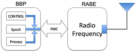
Figure 1.
Communication system model. A block sequence about the communication system model and its architecture.
The BBP stage consisted of the development and coupling of the Serial Communication Protocol (SPI), as well as the programming of the registers to control the flow of data, synchronization, and processing of the data from the BBP to the RABE through the FMC connector, which is responsible for carrying all the bits for the operation of both devices, including the voltage and ground lines.
In the RF stage, the SPI was synchronized to program all the necessary registers in the IC, the DACs, the filtering stage, the preamplifiers, and the local oscillator, which were configured to be tuned at the required frequency. It is noteworthy that each of the configured actions corresponds to the programming of register groups in order to obtain the correct result shown in yellow in Figure 2.
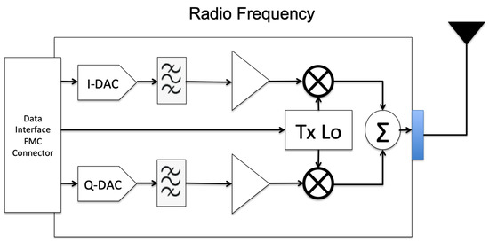
Figure 2.
Radio frequency model. RF PCB scheme and AD9364 architecture.
2.2. RF Stage Design
During the design stage of the RABE subsystem prototype, the necessary requirements for the development of the PCB (Printed Circuit Board) were specified to guarantee correct operation, allowing interoperability between the subsystem devices. The requirements are detailed in Table 1.

Table 1.
General requirements of the RABE.
In general, the design of the RABE features two interfaces; the first one is the digital I/O data, control, and synchronization interfaces between the prototype and the SoC; the second one is the analog RF output with an SMA connector.
The 1U CubeSat standard is restricted to 10 cm2, as can be seen in Figure 3a. Due to this and considering the physical structure of the CubeSat, it is necessary to implement the PCB inside it, leaving the dimensions shown in Figure 3b.
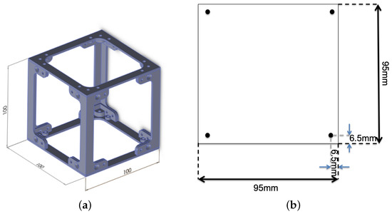
Figure 3.
Structure and PCB measurements in mm. (a) CubeSat structure. (b) PCB size.
The RABE has a read/write register interface carried out via the Serial SPI. Therefore, one of the preliminary tasks was to implement the SPI port in the BBP since it is not a native protocol in the FPGA.
The data lines for the PCB of the RF stage are divided into two sets: the differential and single-ended lines, as shown in Figure 4. The maximum data transfer frequency achieved is 245.76 and 61.44 MHz for the differential bus and single-ended, respectively. However, it depends on the IP-Core processing speed of the SoC and FPGA used by the implementation. The RF output feeds the next stage (it is not the scope of the work) comprised of power amplifiers, filters, and antennas, in order to achieve a high signal-to-noise ratio (SNR) and considering a link range of 2000 km in the free-space Low Earth Orbit (LEO) satellite.
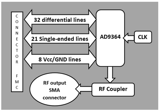
Figure 4.
Schematic design of the RABE. This figure shows how AD9364 is connected to the FMC connector, as well as the FPGA and RF Output to the power amplifier stage (not shown at this work).
The RF stage of the RABE prototype uses the AD9364 transceiver, internally composed of ADC converters, DACs, filters, GPOs, PLLs, and an SPI communication control ports [12], as illustrated in Figure 5.
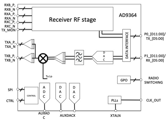
Figure 5.
Block diagram of the IC AD9364. In this figure, the AD9364 manufacturer describes how it connects internally.
In this work, the transmission, data entry, DAC, filters, and SPI serial communication stages are used. The radio transmitter is implemented with the ability to operate in various frequency bands, mainly S-band. In addition to this, the configuration to modify in the application of the IC data such as the transmission power, the filtering, and, most importantly, that the prototype design must comply with the size proposed for the CubeSat standard. The IC AD9364 from Analog Devices® [12] is configured as an RF transceiver, operating in the 0.070 to 6.000 GHz frequency range with the ability to tune the bandwidths (BW) from 0.2 to 56.0 MHz and allowing applications proposed by the manufacturer such as point-to-point communication systems, base stations (BS) for femto/pico/microcells and general-purpose radio systems.
Further, the AD9364 IC is set by reading/writing into the registers set described in [13]. According to the manufacturer, the IC has a list of almost 1014 (0x3F6) 8-bit registers with configuration capabilities intended for diverse applications. These IC-specific application steps are initialization, configuration, transmission, reception, and analog records in reception (see Table 2). Record data flow modes can be: read, write, or both. The SPI port of the AD9364 operates at a recommended maximum speed of 50 MHz, according to the manufacturer’s specifications [12]. However, a frequency of 8 MHz was used for testing purposes in this work to ensure a safe transfer of information to registers.
Table 2.
Functions of the AD9364 registers.
Regarding the operating and configuration modes of the registers, there is a relatively large number of reserved and/or empty positions; thus, in order not to cause improper operation of the system, it is advisable not to refer to them.
To reduce transients while changing the transmission frequency setting on the device, the power to the matching stage on the transmission lines is directly connected to a 1.3 V voltage source. The capacitors, shown in Figure 6, are intended for removing noise and transients at the transmitter output.
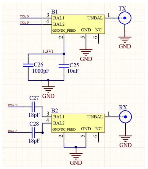
Figure 6.
The RF matching stage, designed to avoid interference for 2–3 GHz.
It is worth mentioning that all the designs, measurements, and tests for the resulting devices were carried out in a test laboratory with a controlled environment (temperature, voltage levels, electromagnetic noise, and electric shocks, etc.) in such a way that the results obtained are completely similar to those obtained by simulations tools.
Design rules concerning the CubeSat standard [14] and PCB design [15] were applied to the electronic design process. The final result was a 6-layer PCB of 10 × 10 cm (see Figure 7); on the other hand, the manufacturer suggests a fixing or soldering area on the PCB with the intention of achieving high performance and achieving adequate operation of the IC [13]. In Table 3, the thickness of the 6 PCB layers is shown.
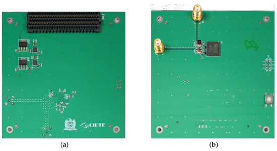
Figure 7.
RABE-printed circuit board. A 3D model of the RABE ((a) top layer and (b) bottom layer).
Table 3.
RABE PCB layers.
Within the PCB, it is intended to integrate devices with the ability that they can be selected (RF switch) and digitally tuned [16] to take advantage of the available space in it and to be able to use different devices such as antennas, amplifiers, and filters in frequency bands that are too far apart from the main one.
The PCB for the radio transmitter was designed using Altium®, a high-end PCB design software package. The simulation of signal behavior on the PCB was carried out using Keysigth® EMPro® and Genesys® tools. The purpose of the simulation was both to validate low levels of electromagnetic interference (EMI) between interconnecting tracks and to avoid radiation to other components included in the board before PCB fabrication.
2.3. Testbed Design
The testbed shown in Figure 8 was integrated to measure the transmission power and frequency values and also to check the operation of the RABE prototype. The hardware devices and software used for the testbed implementation are: Keysigth® N9030A Signal Analyzer, personal desktop computer, Digilent/Xilinx® brand Zedboard test card, RF cables with SMA connector, ethernet cable, RABE prototype, control and programming software for AD9364 IIO Oscilloscope, and IP address monitoring software.
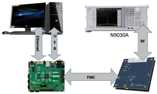
Figure 8.
Testbed block diagram. Configuration for the connection of the test bed for the prototype.
The steps for running the testbed are as follows:
- Download and install the IIO Oscilloscope software on your PC.
- Insert the RABE to the Zedboard through the FMC connector.
- Connect the RF cable from the RABE SMA connector to the N9030A.
- Connect the ethernet and USB cable between the PC and the Zedboard.
- Run the IIO Oscilloscope software on your PC.
- Use the IIO Oscilloscope to configure the transmission frequency, bandwidth, attenuation, and other parameters.
- Configure the N9030A to perform a scan on parameter values close to those set in the previous step.
- Save the data to the N9030A.
3. Results and Discussion
Using the configuration described in Section 2.3, the testbed was implemented to test the RABE prototype, obtaining similar results to those from the IC manufacturer’s test card AD9364 [12].
Two types of experimental measurements were carried out in order to verify the proper operation of the implemented prototype. In both scenarios, the same settings were used for output power, transmission frequency, and bandwidth parameters. As a result, it was noted that RABE output power (Figure 9a) was reduced by 2 dB compared to FMCOMMS4 (Figure 9b), which was 7 dB. It is important to mention that according to the AD9364 datasheet, it is able to transmit with a maximum power of 7.5 dBm when matched to 50 ohms load at 2.4 GHz.
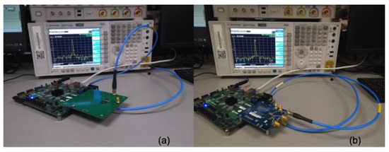
Figure 9.
Implementation of the test bed for the RABE prototype. (a) tests of the manufactured prototype. (b) tests of the FMCOMMS4 card.
Based on the Nyquist noiseless channel, the theoretical maximum bit rate is defined as equal to twice the bandwidth symbol (BW) per second. If each symbol can carry M different distinguishable levels, then each pulse carries log M bits of information, which is described by
Since the bandwidth of the AD9364 ranges from 200 KHz to 56 MHz, the data rate capacity for quaternary modulation, M = 4, will be between 0.800 and 224 Mbps.
In Figure 10, the graph of the data collected in the test bench shows the spectrum transmitted by a signal with a carrier frequency of 2.6095 GHz to verify the correct operation of the design in different frequencies. The spikes shown at 2591 and 2599, are unidentified carriers external to the prototype system. The output power available at the carrier frequency in Figure 10 was −20 dBm, as shown. A Gaussian 3 dB resolution bandwidth (RBW) filter was applied into the signal analyzer followed by a Fast Fourier Transform (FFT) with a BW of 411.9 kHz.
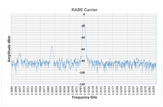
Figure 10.
Spectrum of signal transmitted at 2.6095 GHz. Further processing of the data shows the spectrum of the carrier signal transmitted at 2.6095 GHz.
The BBP was set in a QAM modulation scheme at the testbed (as shown in Figure 11). The resulting modulation process was controlled and synchronized by the BBP to the RABE stage via the FMC connector.
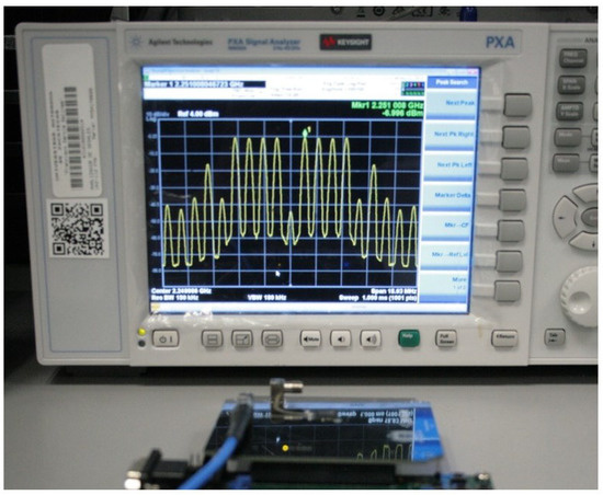
Figure 11.
Signal analyzer, RABE and Zedboard on QPSK. The RABE prototype transmitting with 4-tone QPSK modulation, with 1 MHz frequency separations.
The Total Harmonic Distortion (THD) percentage was measured as described in [17] and is given by
where is the output power of the n-th harmonic in watts, and is the output power of the fundamental frequency in watts.
According to measurements made in the Lab using the N9030A Signal Analyzer, for harmonics, as shown in Table 4, it was found that
Table 4.
Harmonics generated by the RABE at 2.30 GHz.
The distortion values due to the harmonics generated by the transmitter stage could reach values of up to 3.8%, reducing the output power of the RF signal, as shown in Table 4.
Communication systems with a low THD produce less interference between electronic devices connected to or close to the PCB.
In Figure 12, the spectrum generated by the RABE is shown, which was taken directly from the RF output by the N9030A analyzer, all this at a frequency centered at 2.300 GHz, in which it is allowed by the Mexican government for experimental satellite links according to the frequency allocation table [18].
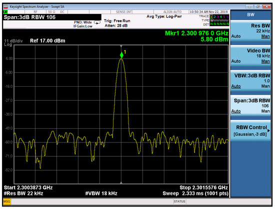
Figure 12.
Spectrum radiated by RABE at 2.300 GHz. Image obtained from the signal analyzer with the prototype transmitting a single tone with a frequency of 2.300 GHz.
On the other hand, it is worth mentioning that the development of the PCB was taking into account the CubeSat standard, with the idea of possible inclusion as a payload in a satellite platform and carrying out transmission tests from space. To ensure that the designed device has a correct performance in space, it is necessary to carry out different types of tests so that the prototype can withstand the working conditions (electromagnetic radiation, thermal gradient) in space and being put into orbit (vibration). Among the tests that the prototype will undergo, we can mention those of electromagnetic compatibility and susceptibility, Total Ionizing Dose (TID), vibration and thermo-vacuum.
Some simulations were carried out, and they were obtained according to the PCB of the manufactured prototype, with the aim of comparing and knowing the radiation generated by inducing an electric current in the transmission lines. These simulations were carried out using the Keysigth® EMPro® software based on the Finite Difference Time Domain Method (FDTD) because it is one of the numerical analysis techniques best used to simulate electrodynamics, as manifested in [19,20,21,22,23,24,25,26,27,28,29,30,31,32,33,34,35].
The simulation was carried out taking into account the Transmission Lines (TL) designed on the RABE prototype PCB towards the RF output. The near field for the present prototype is defined as maximum (wavelength). To perform the simulations, the frequency was defined at 2.3 GHz; therefore, the radiation levels emitted by the TL for the field can be seen in Figure 13a and for the field in Figure 13b.
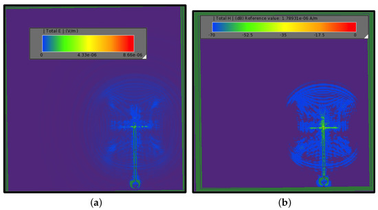
Figure 13.
and field simulations on the RABE transmission line. (a) Electric () field. (b) Magnetic () field.
It can be seen graphically that the radiation levels emitted by the TL of the RABE transmitter do not act as an antenna towards the outside of the PCB with the and fields.
However, when obtaining the Poynting vector with (3), the case is different, because here it can be seen that the radiation pattern exceeds the limits of the PCB.
With the simulations of the and fields, the Poynting vector can be obtained, as can be seen in Figure 14, where gives the measure of rate of energy flow per unit surface area at a point in a uniform plane wave.
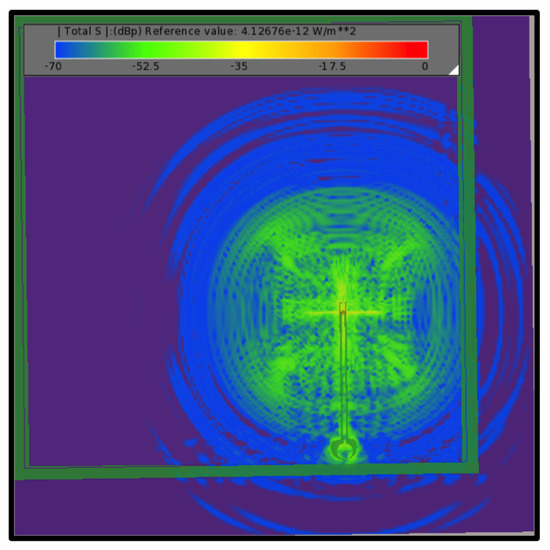
Figure 14.
Poynting Vector.
4. Conclusions
In this paper, the design, construction, verification, and test of a prototype for a reconfigurable radio-transmitter called RABE was presented. The proposed prototype can be used as the communication subsystem in a nanosatellite based on the CubeSat standard. Construction and testing were performed under quality standards in a controlled environment. Results show the correct operation of our card similar to that one commercialized by the IC manufacturer.
The resulting implementation of RABE guarantees the reconfiguration of a nanosatellite communication subsystem. Because of this reconfiguration capacity, it is possible to either have a communication with the terrestrial segment or with other devices orbiting in space, as in the BBP stage, different processing stages can be selected (e.g., modulation scheme). Similarly, the RF stage parameters can be modified (e.g., carrier frequency or transmitter power).
In short, this design allows reducing the number of unnecessary components, optimizing the dimensions of the PCB, and having a weight and size adequate to the specifications of the CubeSat standard.
It is necessary to implement reconfigurable devices and systems externally to a satellite communications subsystem, as shown in the present work and in [10,16], in order to obtain and complement what is stated in these proposals.
It should be noted that power values achieved in the RF output stage of the RABE are sufficient for the subsequent stages of the nanosatellite communications subsystem, which include filters, power amplifiers, and antennas, among others.
However, in the future, it will be necessary to carry out measurements of electromagnetic compatibility and susceptibility to the RABE prototype in order to identify anomalies such as interferences with other devices that make up the satellite. In addition to this, it is recommended to carry out Total Ionizing Dose (TID), Single-Event Effects (SEEs), and vibration and thermal vacuum tests to verify the robustness of the design when it comes to being placed in orbit. Furthermore, as future work, it is recommended that both the baseband processing, control, and reconfiguration stage and the RF stage could be integrated on a single PCB trying to minimize the size of the communication system and at the same time optimizing the operating speed.
Author Contributions
J.L.A.-F. has completed the design and manufacture of the prototype, with the accompaniment of J.A.C. and V.I.R.-A. and under the supervision of J.F.-T., J.S. and L.S.-E.; J.L.A.-F., J.F.-T., L.S.-E., R.P.-M., V.I.R.-A. and J.S. made the translation for the present work; J.L.A.-F., J.F.-T. and J.S. participated in the design of this paper. All authors have read and agreed to the published version of the manuscript.
Funding
The authors would like to thank the Mexican National Council for Science and Technology (CONACYT) and the Mexican Space Agency (AEM) for supporting project 292793 through the AEM-CONACYT Sectorial Fund for Research and Development in Space Activities, from which this article emerged as a result.
Data Availability Statement
The data presented in this study are available on request from the corresponding author.
Acknowledgments
The authors would like to thank the Center for Research, Innovation and Development in Telecommunications (CIDTE) of the Autonomous University of Zacatecas (UAZ) for the support provided for the use of the necessary infrastructure for the development of this project. J.L.A.-F. thanks PRODEP for the support provided to carry out doctoral studies at the Autonomous University of Zacatecas.
Conflicts of Interest
The authors declare that they have no competing interests.
Abbreviations
The following abbreviations are used in this manuscript:
| CAD | Computer-Aided Design |
| PCB | Printed Circuit Board |
| GPP | General Purpose Processor |
| DSP | Digital Signal Processor |
| FPGA | Field Programmable Gate Array |
| SDR | Software-Defined Radio |
| SoC | System on a Chip |
| IC | Integrated Circuit |
| GHz | Gigahertz |
| MHz | Megahertz |
| COTS | Commercial-Off-The-Shelf |
| RF | Radio Frequency |
| DDC | Digital Down Converter |
| VHDL | Vhsic Hardware Description Language |
| BBP | BaseBand Processor |
| RABE | Reconfigurable Analog Back-End |
| SMA | SubMiniature version A |
| FMC | FPGA Mezzanine Card |
| SPI | Serial Communication Protocol |
| DAC | Digital–Analog Converter |
| I/O | Input/Output |
| SNR | Signal-to-Noise Ratio |
| LEO | Low Earth Orbit |
| km | Kilometer |
| GPO | General-Purpose Output |
| PLL | Phase-Locked Loop |
| BS | Base Stations |
| EMI | ElectroMagnetic Interference |
| BW | BandWidth |
| KHz | Kilohertz |
| RBW | Resolution BandWidth |
| FFT | Fast Fourier Transform |
| THD | Total Harmonic Distortion |
References
- Golkar, A.; Lluch, I. The federated satellite systems paradigm: Concept and business case evaluation. Acta Astronaut. 2015, 111, 230–248. [Google Scholar] [CrossRef]
- Bard, J.; Kovarick, V.J. Software Defined Radio. In The Software Communications Architecture; Wiley: Hoboken, NJ, USA, 2007; p. 439. [Google Scholar]
- Akhtyamov, R.; Lluch, A.; Matevosyan, H.; Knoll, D.; Pica, U.; Lisi, M.; Golkar, A. An implementation of software defined radios for federated aerospace networks: Informing satellite implementations using an inter-balloon communications experiment. Acta Astronaut. 2016, 123, 470–478. [Google Scholar] [CrossRef]
- Maheshwarappa, M.R.; Bowyer, M.; Bridges, C. Software defined radio (SDR) architecture to support multi-satellite communications. In Proceedings of the IEEE Aerospace Conference, Big Sky, MT, USA, 7–14 March 2015; pp. 1–10. [Google Scholar]
- Tian, F.; Li, H.; Yuan, L. Design and implementation of AD9361-based software radio receiver. J. Wirel. Commun. Netw. 2019, 2019, 95. [Google Scholar] [CrossRef] [Green Version]
- Maheshwarappa, M.R.; Bowyer, M.; Bridges, C. Software defined radio (SDR) for parallel satellite reception in mobile/deployable ground segments. In Proceedings of the 29th Annual AIAA/USU Conference on Small Satellites, Santa Clara, CA, USA, 8–13 August 2015; pp. 1–12. [Google Scholar]
- Kamaleldin, A.; Hosny, S.; Mohamed, K.; Gamal, M.; Hussien, A.; Elnader, E.; Shalash, A.; Obeid, A.; Ismail, Y.; Mostafa, H. A Reconfigurable Hardware Platform Implementation for Software Defined Radio Using Dynamic Partial Reconfiguration on Xilinx Zynq FPGA. In Proceedings of the IEEE 60th International Midwest Symposium on Circuits and Systems (MWSCAS), Boston, MA, USA, 6–9 August 2017; pp. 1540–1543. [Google Scholar] [CrossRef]
- Haider, A.; Anwar, A.; Rizwan Mughal, M.; Reyneri, L.; Sansoe, C.; Praks, J. Modular Design of RF Front End for a Nanosatellite Communication Subsystem Tile Using Low-Cost Commercial Components. Int. J. Aerosp. Eng. IJAE 2019, 2019, 8174158. [Google Scholar]
- Flores-Troncoso, J.; Ibarra-Delgado, S.; Sandoval-Arechiga, R.; Rodriguez-Abdala, V.; Garcia-Luciano, L. Desarrollo de IP-Cores para un prototipo de sistema de radiocomunicación satelital en banda base definido por software. In Hacia el Desarrollo Espacial en México; CONCYTEQ: Queretaro, Mexico, 2017; pp. 49–60. [Google Scholar]
- Hofmann, A.; Glein, R.; Frank, L.; Wansch, R.; Heuberger, A. Reconfigurable on-board processing for flexible satellite communication systems using FPGAs. In Proceedings of the 2017 Topical Workshop on Internet of Space (TWIOS), Phoenix, AZ, USA, 15–18 January 2017; pp. 1–4. [Google Scholar] [CrossRef]
- GOMS. Space Qualified Software Defined Radio (SDR) Platform for Sensing and Communication Applications Using Powerful and Advanced FPGA Technology. Available online: https://gomspace.com/Shop/payloads/software-defined-radio.aspx (accessed on 15 June 2018).
- Analog, D. RF Agile Transceiver. Available online: https://www.analog.com/media/en/technical-documentation/data-sheets/AD9364.pdf (accessed on 20 August 2019).
- Analog, D. AD9364 Register Map Reference Manual. Available online: https://www.analog.com/media/cn/technical-documentation/user-guides/AD9364_Register_Map_Reference_Manual_UG-672.pdf (accessed on 20 August 2019).
- CubeSat. Origin of the New Space Revolution. Available online: http://www.cubesat.org/ (accessed on 18 January 2018).
- IPC. Generic Standard on Printed Board Design. Available online: http://www.ipc.org/TOC/IPC-2221.pdf/ (accessed on 18 January 2018).
- Jaschke, A.; Tessema, M.; Schühler, M.; Wansch, R. Digitally tunable bandpass filter for cognitive radio applications. In Proceedings of the 2012 IEEE 17th International Workshop on Computer Aided Modeling and Design of Communication Links and Networks (CAMAD), Barcelona, Spain, 17–19 September 2012; pp. 338–342. [Google Scholar] [CrossRef]
- Briceño Marquez, J.E. Principios de las Comunicaciónes; Facultad de Ingenieria, Publicaciones: Merida, Venezuela, 2012. [Google Scholar]
- Cuadro Nacional de Atribucion de Frecuencias; Secretaria de Comunicaciones y Transportes. Atribución del Espectro Radioeléctrico Para los Servicios de Radiocomunicación: Mexico. 1999. Available online: https://www.itu.int/ITU-D/study_groups/SGP_1998-2002/JGRES09/pdf/mexico1.pdf (accessed on 18 January 2018).
- Yee, K. Numerical solution of initial boundary value problems involving maxwell’s equations in isotropic media. IEEE Trans. Antennas Propag. 1966, 14, 302–307. [Google Scholar] [CrossRef] [Green Version]
- Taflove, A.; Brodwin, M.E. Numerical Solution of Steady-State Electromagnetic Scattering Problems Using the Time-Dependent Maxwell’s Equations. IEEE Trans. Microw. Theory Tech. 1975, 23, 623–630. [Google Scholar] [CrossRef]
- Nagra, A.S.; York, R.A. FDTD analysis of wave propagation in nonlinear absorbing and gain media. IEEE Trans. Antennas Propag. 1998, 46, 334–340. [Google Scholar] [CrossRef]
- Taflove, A. Application of the Finite-Difference Time-Domain Method to Sinusoidal Steady-State Electromagnetic-Penetration Problems. IEEE Trans. Electromagn. Compat. 1980, EMC-22, 191–202. [Google Scholar] [CrossRef]
- Umashankar, K.; Taflove, A. A novel method to analyze electromagnetic scattering of complex objects. IEEE Trans. Electromagn. Compat. 1982, EMC-24, 397–405. [Google Scholar] [CrossRef]
- Kriegsmann, G.A.; Taflove, A.; Umashankar, K.R. New formulation of electromagnetic wave scattering using an on-surface radiation boundary condition approach. IEEE Trans. Antennas Propag. 1987, AP-35, 153–161. [Google Scholar] [CrossRef]
- Kunz, K.S.; Lee, K.M. A three-dimensional finite-difference solution of the external response of an aircraft to a complex transient EM environment: Part II-Comparison of predictions and measurements. IEEE Trans. Electromagn. Compat. 1978, EMC-20, 333–341. [Google Scholar] [CrossRef]
- Jurgens, T.G.; Taflove, A.; Umashankar, K.; Moore, T.G. Finite-Difference Time-Domain Modeling of Curved Surfaces. IEEE Trans. Antennas Propag. 1992, 40, 357–366. [Google Scholar] [CrossRef]
- Ramahi, O.M. The complementary operators method in FDTD simulations. IEEE Antennas Propag. Mag. 1997, 39, 33–45. [Google Scholar] [CrossRef]
- Moore, T.G.; Blaschak, J.G.; Taflove, A.; Kriegsmann, G.A. Theory and Application of Radiation Boundary Operators. IEEE Trans. Antennas Propag. 1988, 36, 1797–1812. [Google Scholar] [CrossRef]
- Toland, B.; Houshmand, B.; Itoh, T. Modeling of Nonlinear Active Regions with the FDTD Method. IEEE Microw. Guid. Wave Lett. 1993, 3, 333–335. [Google Scholar] [CrossRef]
- Umashankar, K.R.; Piket-May, M.J.; Taflove, A. FDTD Analysis of Electromagnetic Wave Radiation from Systems Containing Horn Antennas. IEEE Trans. Antennas Propag. 1991, 39, 1203–1212. [Google Scholar] [CrossRef]
- Joseph, R.M.; Hagness, S.C.; Taflove, A. Direct time integration of Maxwell’s equations in linear dispersive media with absorption for scattering and propagation of femtosecond electromagnetic pulses. Opt. Lett. 1991, 16, 1412. [Google Scholar] [CrossRef]
- Lee, J.F.; Mittra, R. A Hybrid Yee Algorithm/Scalar-Wave Equation Approach. IEEE Trans. Microw. Theory Tech. 1993, 41, 1593–1600. [Google Scholar] [CrossRef]
- Luebbers, R.; Hunsberger, F.R.; Kunz, K.S.; Standler, R.B.; Schneider, M. A Frequency-Dependent Finite-Difference Time-Domain Formulation for Dispersive Materials. IEEE Trans. Electromagn. Compat. 1990, 32, 222–227. [Google Scholar] [CrossRef]
- Taflove, A.; Umashankar, K.R.; Beker, B.; Harfoush, F.; Yee, K.S. Detailed FD-TD Analysis of Electromagnetic Fields Penetrating Narrow Slots and Lapped Joints in Thick Conducting Screens. IEEE Trans. Antennas Propag. 1988, 36, 247–257. [Google Scholar] [CrossRef]
- Mur, G. Absorbing Boundary Conditions for the Finite-Difference Approximation of the Time-Domain Electromagnetic-Field Equations. IEEE Trans. Electromagn. Compat. 1981, EMC-23, 377–382. [Google Scholar] [CrossRef]
Publisher’s Note: MDPI stays neutral with regard to jurisdictional claims in published maps and institutional affiliations. |
© 2022 by the authors. Licensee MDPI, Basel, Switzerland. This article is an open access article distributed under the terms and conditions of the Creative Commons Attribution (CC BY) license (https://creativecommons.org/licenses/by/4.0/).