Abstract
As a promising candidate in space radiation hardened applications, silicon-on-insulator (SOI) devices face the severe problem of total ionizing dose (TID) radiation because of the thick buried oxide (BOX) layer. The direct-current current–voltage (DCIV) method was applied for studying TID radiation of SOI metal–oxide–semiconductor field–effect transistors (MOSFETs) with different manufacture processes. It is found that the peak of high-voltage well (PX) devices shows a larger left-shift and a slower multitude increase along with radiation dose, compared with that of low-voltage well (PV) devices. It is illustrated that the high P-type impurity concentration near back interface makes it more difficult to break up silicon hydrogen bonds, which gives the PX devices superiority in resisting the build-up of interface traps. The study results indicate that increasing doping concentration of the body region near the back-gate interface might be an alternative radiation hardening technique of SOI MOSFET devices to avoid the parasitic back transistors’ leakage.
1. Introduction
Due to the dielectrically isolated, reduced collection volume, and the reduced p–n junction area, silicon on insulator (SOI) transistors have significantly excellent single event effect (SEE) immunity and dose rate radiation response [1,2,3]. Silicon on insulator (SOI) technology has been a promising candidate in space and military radiation hardened applications. Unfortunately, the SOI devices have been faced with the severe problem of total ionizing dose (TID) radiation because of the thick buried oxide (BOX) layer [2,4]. The full dielectric isolation could introduce an additional source for radiation-induced trapped charge. Excessive charge trapping of buried oxide can invert the back-channel interface, forming a parasitic conductive path from source to drain. This could lessen the advantages of space and military applications of the SOI technology [3,5]. Therefore, it is essential to study the TID response of SOI technologies.
Many efforts have been made to explore the origin of the degradation of SOI devices under TID radiation [4,6,7]. The two primary types of TID radiation-induced charges are oxide-trapped charge and interface-trap charge, which can cause the threshold voltage to shift and the leakage current to increase [2,3,7]. In order to further study the mechanisms of TID-induced degradation, the separation of the interface trap charge from the trap charge effectively is essential. Several techniques [8,9,10,11,12] have been proposed for the determination of interface trap concentration. As the feature size of transistors have scaled to deep sub-half-micron, conventional methods such as the capacitor-voltage (C-V) and mid-gap voltage methods have been found to be not suitable [13]. The large thickness of BOX renders some alternating current (AC) methods, such as charge pumping and dynamic transconductance, insensitive and unavailable [14]. The direct-current current–voltage (DCIV) technique was proposed as a sensitive and powerful technology for the determination of interface trap concentration in SOI devices [15,16]. The superiority of the DCIV method over conventional methods is that this method can be utilized for detecting the energy distribution of the interface trap density near the mid-gap and it is suitable for the characterization of back interface traps in SOI devices with a thick buried oxide layer. The DCIV method has been successfully applied in the extraction of interface-trap energy distribution after the radiation effect and hot carrier degradation in our previous works [17,18]. Hence, the DCIV method may be a good choice for studying the TID radiation of SOI MOSFET devices.
The DCIV technique is used to characterize the interface trap density by detecting the recombination current associated with the interface traps based on Shockley–Read–Hall steady-state recombination kinetics [9,19,20]. When an appropriate voltage is applied to the back gate, the back channel will be depleted totally and the electrons and holes near the interface traps at the back interface will be adequate. The recombination rate of interface traps will reach the maximum and the density of interface traps will be calculated according to the SRH recombination theory [19,20,21]. In this paper, based on the DCIV method, the radiation characteristics of SOI NMOSFETs with different process conditions are investigated. The results can be used to provide a comprehensive basic overview on DCIV experimental measurements and analysis of interface traps in SOI MOSFETs. The experimental details and results are given in Section 2. The discussion and analysis are implemented with the aid of a technology computer aided design (TCAD) simulator in Section 3, in detail.
2. Experimental Results
The devices under test in this work were fabricated in 0.18 μm H-gate SOI technology with a top silicon film thickness of about 280 nm and a buried oxide thickness of 350 nm, as shown in Figure 1. The gate oxide layer with the thickness of 3 nm was formed by the thermal oxidation process. The poly silicon/thermal oxide was used for the gate stack. The channel width and length of NMOSFET are W = 100 μm and L = 10 μm respectively. There are two kinds of devices under test; one is the PV device with a low-voltage well (PV) process, and the other is the PX device with a high-voltage well (PX) process. The dopant profile of boron in the whole silicon layer is special by the means of multiple ion implantations. The high energy boron ions were implanted to form the p-well. Middle energy ions and low energy ions were used for the definition of the doping profile of top silicon. For PX devices and PV devices, the dopant profile of boron in the whole silicon layer is special. Finally, the doping concentration near the back interface is on the order of 1 × 1017 cm−3 in PX devices and on the order of 1 × 1018 cm−3 in PV devices. Transistors were irradiated at room temperature using a 60Co gamma-ray irradiation source, at a typical dose rate of 50 rad (Si)/s. The bias configurations during irradiation were set at the on state with the gate at an operating voltage and the source and drain grounded. DCIV measurements of fresh and irradiated SOI NMOSFETs were performed using a Keithley 4200 semiconductor parameter analyzer; the DCIV measurement setup is shown in Figure 1. The details and principles of the DCIV measurement have been presented in our previous work [17]. Here, we describe the DCIV testing process briefly. The body-to-drain junction and body-to-source junction of the MOS transistors are forward biased at the appropriate values to increase the injected minority carrier concentration greatly and to ensure the adequate recombination at the back-gate interface traps. The source and drain terminals were biased at 0.48 V in this work. The DCIV current is monitored when the back-gate voltage is scanned from a negative to positive voltage and it reaches the maximum value when the back-gate channel is depleted totally. The front gate voltage VFG is 1.8 V. The front gate voltage is held at an inversion, thus making sure that the source/body and drain/body junctions “extend” under the entire front gate, forming the same and uniform inversion layer and junction.
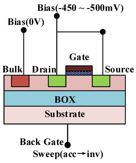
Figure 1.
A two-dimensional (2-D) structure and the DCIV measurement setup of the SOI NMOSFETs.
Figure 2 shows the pre- and post-irradiation transfer characteristics of the SOI NMOSFETs as a function of the radiation dose. The Id-Vgs curves in Figure 2 are plotted in linear (right) and logarithmic (left) scale. As shown in Figure 2, a slight decrease in Vth occurs after TID radiation. This occurs in the irradiated devices because of the trapped charges in the gate stack. The presented small Vth degradation might be due to thin gate oxide. On the other hand, the total dose irradiation brings a slight increase in the drive current as shown in Figure 2, which might directly be impacted by Vth degradation. It is clear that the irradiation-induced leakage current increases significantly along with the radiation dose, which is regularly observed in SOI devices [4]. The large leakage current is not only related to the interface traps at the gate-oxide/silicon interface, but also to the oxide traps in the buried oxide and the interface trap charge at the buried-oxide/silicon interface. The thick buried oxide layer accumulates a large amount of fixed charge, which leads to a parasitic back channel. The interface traps at the buried-oxide/silicon interface are more likely to cause more current leakage. Therefore, it is necessary to study the trap charge near the back channel. The direct-current current–voltage (DCIV) method was applied for studying TID radiation of SOI MOSFETs with different manufacture processes.
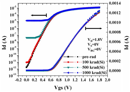
Figure 2.
The pre- and post-irradiation transfer characteristics in the linear (right) and logarithmic (left) scale of the SOI NMOSFETs as a function of radiation dose.
Figure 3 depicts the experimental bulk current versus the back-gate voltage (IB-VBG) characteristics under varying radiation doses in the PX and PV devices. As shown in Figure 3, the DCIV current versus the sweeping of the back-gate bias voltage exhibits a bell-shape curve. The bulk current (IB) reaches the maximum when a voltage depleting fully back channel is applied to the back-gate terminal of SOI NMOSFETs. It is shown that the DCIV peak current (IB-peak) is elevating and the back-gate voltage at the peak current (VBG-peak) shifts left as the radiation dose increases, which is also observed in Ref. [22]. After the irradiation of 1 Mrad(Si), IB-peak increased nearly one order of magnitude and VBG-peak shifted by tens of volts. Specifically, IB-peak increased from 1.99 × 10⁻⁸ A to 1.36 × 10⁻⁷ A and VBG-peak shifted from +20 V to −12 V for PV devices. IB-peak increased from 2.67 × 10⁻⁷ A to 1.27 × 10⁻⁷ A and VBG-peak shifted from +26 V to −10 V for PX devices. It is considered that the increase in IB-peak along with the dose is related to radiation-induced interface traps and the shift of the peak along with the dose might be the result of the oxide trap charge.
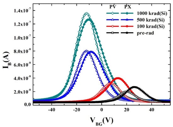
Figure 3.
The experimental bulk current versus the back-gate voltage (IB-VBG) characteristics under varying radiation doses: pre-rad (0 krad(Si)), 100 krad(Si), 500 krad(Si), 1000 krad(Si) in the devices with high-voltage well (PX) process (solid symbol) and low-voltage well (PV) technology (open symbol). VD, and VS were biased at 0.48 V; VFG was biased at 1.8 V.
The IB-peak of the PX devices is significantly larger than that of the PV devices before TID radiation and at the radiation dose of 100 krad(Si). However, with the increase in radiation dose, the DCIV peak current (IB-peak) of PV devices is almost equal to the current value of PX devices at 500 krad(Si), and the IB-peak of PV devices is even more than that of PX devices at 1000 krad(Si). The increase in the DCIV peak current (IB-peak) along with the radiation dose in PV devices is faster than that of PX devices. It is also observed that the VBG-peak of PX devices is always larger than that of PV devices. The peak voltage (VBG-peak) of PX devices is significantly higher than that of PV devices before irradiation. Along with the radiation dose increasing, the peak voltage (VBG-peak) of PX devices is closer to the peak voltage of PV devices. In the case of 1000 krad(Si) irradiation, the peak voltage (VBG-peak) of PX devices is only slightly higher than that of PV devices. The different manufacturing process could induce a different interface quality and defect states. This might be related to the change of IB-peak and VBG-peak.
3. Discussion
As is well known, the radiation response of SOI MOSFETs could induce the oxide traps (Not) in buried-oxide and interface traps (Nit) at the Si/SiO2 interface [2,3]. The variations of DCIV curves might be related to the two kinds of traps. To further analyze the effect of TID radiation on DCIV curves, the Sentaurus TCAD simulations were carried out. Figure 4a shows the simulated three-dimensional (3-D) structure and the partial enlargement is shown in the lower left corner of the image. Figure 4b shows a two-dimensional (2-D) cross-sectional view cut along the A-A’ direction. The specific doping concentration distribution and geometric parameters of generated SOI NMOSFETs are summarized in Table 1. The Sdevice simulator is used to simulate the DCIV performance of transistors. On the basis of the physical mechanism, the physical models used for the Sdevice simulator are: (1) the band gap model, (2) the Shockley–Read–Hall (SRH) generation–recombination model, (3) the mobility degradation model: doping-dependent model, high field saturation model and enormal model, and (4) the band-to-band tunneling model. In this simulation, the electron and hole capture cross section is set as 3.0 × 10⁻¹⁵ cm−2. Similar parameters can be found in previous literatures and their reasonability has been verified [22,23,24]. In this simulation, the oxide trap density (Not) is varied from 1 × 1016 cm−3 to 1 × 1017 cm−3 and the interface trap density (Nit) is changed from 1 × 1010 cm−2 to 8 × 1010 cm−2; these are set according to the previous literature [8]. These values are also consistent with our theoretical calculations [17]. In our previous work [17], the values of electron and hole capture cross sections have been used and verified. The interface trap densities at different doses were calculated by fitting our experimental data and SRH recombination theory. The calculated Nit was 1.28 × 1010 cm−2 at pre-radiation and 7.86 × 1010 cm−2 at a 1Mrad(Si) radiation dose. The value of Nit raised linearly along with the radiation dose at an approximate rate of 6.58 × 109 cm−2 per 100 krad(Si). The devices used in the previous work and the devices used in this work are manufactured by the same process, so it is considered that the previous calculated Nit is very suitable for the simulation work of this paper.
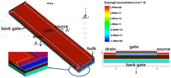
Figure 4.
180 nm H-gate silicon on insulator (SOI) N-type MOSFET simulation model. (a) 3-D structure (b) 2-D cross-section view cut along the A-A’ direction.

Table 1.
Structure and process parameters in the simulation devices.
Figure 5 depicts the simulated DCIV curves after the oxide and interface traps were introduced to the TCAD simulator. As shown in Figure 5a, the shifts of the DCIV curves and the rising of the IB-peak occurred along with the elevating of the introduced oxide traps and interface traps, which is in good agreement with the change trend of the experimental data in Figure 3. In detail, the value of IB-peak increases from 1 × 10⁻⁷ A to 4.5 × 10⁻⁷ A and peak voltage VBG-peak shifts from +20 V to −15 V when the interface trap density and the oxide trap density (Not) increase from 1 × 1010 cm−2 to 8 × 1010 cm−2 and from 1 × 1016 cm−3 to 1 × 1017 cm−3 respectively. Furthermore, the DCIV curve, after only the interface traps are introduced, is also simulated, and the simulated result is shown in Figure 5b. It is observed that only the DCIV current increases without a shift of the DCIV peak. As reported in the previous work [22], bulk current is mainly attributed to the recombination of minority electrons from the n+ source and n+ drain and majority holes in the p-type body when the back gate is swept from accumulation to inversion. The interface traps at the back-gate interface of Si/SiO2 play the roles of recombination centers. The recombination current (IB) generates due to the recombination of electrons injected from source and drain regions and holes from the body region. The recombination current flows from the body region to the source region and drain region. In the process of recombination, the recombination current is dominated in the DCIV current and could be characterized by the bulk current (IB). The DCIV peak current IB-peak could be an indirect characterization of the density of interface traps [25]. The simulation results in Figure 5 are indicative of the increasing of the DCIV peak current, as the dose is related to the interface trap charge induced by the total dose radiation. The shift of peak voltage VBG-peak in Figure 5 could sufficiently indicate the role of radiation-induced traps.
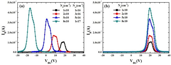
Figure 5.
Simulated IB-VBG characteristics (a) with varying interface trap densities from 1 × 1010 cm−2 to 8 × 1010 cm−2 and oxide trap densities from 1 × 1010 cm−3 to 1 × 1010 cm−3 (b) with varying interface trap densities from 1 × 1010 cm−2 to 8 × 1010 cm−2.
After TID radiation, many electrons and holes are generated in the oxide layer. Because the mobility of electrons in the oxide layer is much greater than that of holes, electrons will be swept out of the oxide layer quickly. The hole will move towards the interface of Si-SiO2. In the moving process, the holes could combine with the oxygen vacancy in the oxide layer. The strained silicon–silicon bonds break down and the positive oxide trapped charge is produced [26]. The holes also react with the hydrogen containing oxide defects or dopant-H complexes during the holes’ transporting, and then lots of protons are released. The protons, moving to the Si/SiO2 interface, can remove hydrogen atoms from H-passivated dangling bonds, forming a large number of interface traps [27,28].
Figure 6 gives the peak current IB-peak and the peak voltage VBG-peak as functions of the irradiation dose in PX devices and PV devices, which are extracted from the DCIV curves shown in Figure 3. This is a clear comparison of DCIV curves between PV devices and PX devices under irradiation. In PX devices, a large dose of P-well ion implantation induces a high impurity concentration near the back interface. When the back-gate voltage is biased at VBG-peak, the surface channel would be depleted fully and the electrons and holes near interface traps would be adequate. The recombination rate of electrons and holes would reach the maximum. Compared with PV devices, the higher P-type impurity concentration in PX devices makes it harder to deplete the surface channel. The VBG-peak of fresh PX devices would be higher than that of fresh PV devices, which is observed in Figure 6. As mentioned above, the bulk current is mainly dependent on the interface traps. The process-induced Si dangling bonds at the Si/BOX interface can perform an effective role in the recombination of electrons and holes when the surface channel is just depleted fully, contributing to the DCIV peak current of fresh samples. It is inferred from the higher IB-peak of fresh PX devices, shown in Figure 6, that instinct interface traps at the Si-film/BOX interface induced by the PX process are more evident than those induced by the PV process, which might be due to the manufacture process of P-type well.
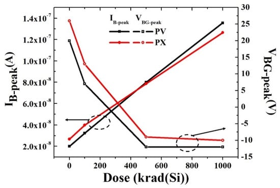
Figure 6.
The experimental peak current IB-peak and peak voltage VBG-peak as functions of radiation dose in the devices with a high-voltage well (PX) process (red line) and a low-voltage well (PV) technology (black line).
We performed a process simulation according to the actual process parameters in PX devices and PV devices by the Sprocess simulator. Figure 7 shows the simulated net carrier concentration profile in the whole silicon from the gate oxide/silicon (Gox/Si) front interface to the buried oxide/silicon (Box/Si) back interface. It is shown that the electron concentration at the Box/Si interface of PX devices is significantly lower than that of PV devices. The consensus of interface-trap creation during radiation is that it is a two-stage process [29,30]. Radiation-generated holes transport through oxide and interact with defect sites containing hydrogen in the oxide layer, releasing the hydrogen as protons H+. Protons then are transported to the interface where they can depassivate Si-H bonds with the aid of electrons, creating interface traps via the following reaction: . In PX devices, a special high P-type doping concentration at the back interface results in few electrons at the back interface. The reaction between protons and silicon hydrogen bonds in the second stage would be limited due to a smaller number of electrons. Thus, the build-up of interface traps during radiation could be suppressed by insufficient electrons due to heavy impurity doping near the back interface. As illustrated in Figure 6, despite the large initial current, the increase in the DCIV peak current (IB-peak) along with the radiation dose in PX devices is slower than that of PV devices. The peak current value is almost equal at 500 krad(Si), and IB-peak of PV devices is even more than that of PX devices at 1000 krad(Si).
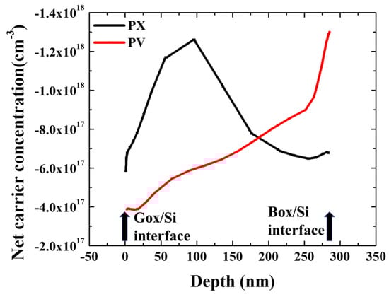
Figure 7.
The simulated net carrier concentration profile in the whole silicon from the gate oxide/silicon (Gox/Si) front interface to the buried oxide/silicon (Box/Si) back interface in PX devices and PV devices.
With the same SOI manufacturing process, the formation of oxide traps in PV devices and PX devices may be assumed to be identical. As mentioned above, interface traps could be built up during radiation, which is related to the impurity concentration of P-type well. Both positive oxide traps and negative interface traps induce the depletion of the back channel, shifting the peaks of DCIV curves. The radiation-induced negative interface traps could compromise the shift of the peak voltage caused by the radiation-induced positive oxide traps in the buried oxide. Compared with PV devices, the higher impurity doping concentration of PX devices results in fewer interface traps. In PX devices, the shift of VBG-peak is mainly attributed to positive oxide traps and is slightly compromised by negative interface traps. The shift of VBG-peak would be relatively larger than PV devices, along with the radiation dose increasing. It is shown in Figure 6 that the change of VBG-peak in PX devices is relatively larger than PV devices along with the radiation dose, although PX devices reveal a larger VBG-peak than that of PV devices, both before and after radiation. Before irradiation, the peak voltage (VBG-peak) of PX devices is significantly higher than that of PV devices. At 1000 krad(Si) irradiation, the peak voltage (VBG-peak) of PX devices is slightly higher than that of PV devices. Specifically, VBG-peak of PX device declined from 26 V to −10 V while VBG-peak of PV device decreased from 20 V to −12 V after suffering from 1000 krad(Si) radiation. The difference in VBG-peak variation as a dose between PX devices and PV devices also indicates that increasing the impurity concentration could resist the build-up of interface traps during radiation.
4. Conclusions
In this work, we investigated DCIV curves of irradiated SOI NMOSFETs with the PV and PX process. DCIV curves at high radiation doses exhibit significant shifts in peak voltage, which is related to the evolution of the oxide trap charge. Meanwhile, the magnitude of DCIV curves also exhibits a rise with the TID dose, indicating the increase in interface traps under irradiation. Furthermore, the increase in the peak current as the TID radiation dose in PX devices is slower than that of PV devices. The diversity of DCIV curves for the devices with PX and PV processes is mainly introduced by the variation of impurity concentration at the back-channel surface. Increasing impurity concentration at the back-channel surface can decline the electrons at the surface of the back channel, resulting in the build-up of interface traps being suppressed. It is inferred that increasing the impurity concentration at the back-channel surface might be a technique to improve radiation hardness in SOI MOS devices.
Author Contributions
Conceptualization, Y.L., X.L. and C.Z.; Data curation, Y.L. and L.G.; Funding acquisition, X.L.; Methodology, Y.L., X.L., C.Z., W.Y., Y.Z. and D.L.; Project administration, Z.H., C.Z. and J.L.; Supervision, X.L. and C.Z.; Writing—original draft, Y.L.; Writing—review & editing, Y.L., X.L. and C.Z. All authors have read and agreed to the published version of the manuscript.
Funding
This work was supported by the National Natural Science Foundation of China (Grant No. 61804168).
Conflicts of Interest
The authors declare no conflict of interest.
References
- Schwank, J.R.; Ferlet-Cavrois, V.; Shaneyfelt, M.R.; Paillet, P.; Dodd, P.E. Radiation Effects in SOI Technologies. IEEE Trans. Nucl. Sci. 2003, 50, 522–538. [Google Scholar] [CrossRef]
- Ferlet-Cavrois, V.; Colladant, T.; Paillet, P.; Leray, J.L.; Musseau, O.; Schwank, J.R. Worst-case bias during total dose irradiation of SOI transistors. IEEE Trans. Nucl. Sci. 2000, 47, 2183–2188. [Google Scholar] [CrossRef]
- Barnaby, H.J. Total-Ionizing-Dose Effects in Modern CMOS Technologies. IEEE Trans. Nucl. Sci. 2006, 53, 3103–3121. [Google Scholar] [CrossRef]
- Ning, B.; Bi, D.; Huang, H.; Zhang, Z.; Hu, Z.; Chen, M.; Zou, S. Bias dependence of TID radiation responses of 0.13 μm partially depleted SOI NMOSFETs. Microelectron. Reliab. 2013, 53, 259–264. [Google Scholar] [CrossRef]
- Alles, M.L.; Schrimpf, R.D.; Reed, R.A.; Massengill, L.W.; Weller, R.A.; Mendenhall, M.H.; Ball, D.R.; Warren, K.M.; Loveless, T.D.; Kauppila, J.S.; et al. Radiation hardness of FDSOI and FinFET Technologies. In Proceedings of the 2011 IEEE International Soi Conference, Tempe, AZ, USA, 3–6 October 2011. [Google Scholar] [CrossRef]
- Yue, J.; Sinha, S. Enhanced hole and interface trap generation in plasma damaged Bulk and SOI MOSFETs under total dose irradiation. In Proceedings of the 3rd International Symposium on Plasma Process-Induced Damage, Honolulu, HI, USA, 4–5 June 1998; pp. 22–25. [Google Scholar] [CrossRef]
- Alles, M.L.; Hughes, H.L.; Ball, D.R.; Mcmarr, P.J.; Schrimpf, R.D. Total-Ionizing-Dose Response of Narrow, Long Channel 45 nm PDSOI Transistors. IEEE Trans. Nucl. Sci. 2014, 61, 2945–2950. [Google Scholar] [CrossRef]
- Zhang, E.X.; Fleetwood, D.M.; Duan, G.X.; Zhang, C.X.; Francis, S.A.; Schrimpf, R.D. Charge Pumping Measurements of Radiation-Induced Interface-Trap Density in Floating-Body SOI FinFETs. IEEE Trans. Nucl. Sci. 2012, 59, 3062–3068. [Google Scholar] [CrossRef]
- Neugroschel, A.; Sah, C.T.; Han, K.M.; Carroll, M.S.; Nishida, T.; Kavalieros, J.T.; Lu, Y. Direct-Current Measurements of Oxide and Interface Traps on Oxidized Silicon. IEEE Trans. Electron Devices 1995, 42, 1657–1662. [Google Scholar] [CrossRef]
- Groeseneken, G.; Maes, H.E.; Beltran, N.; Dekeersmaecker, R.F. A Reliable Approach to Charge-Pumping Measurements in Mos-Transistors. IEEE Trans. Electron Devices 1984, 31, 42–53. [Google Scholar] [CrossRef]
- Jun, B.; Fleetwood, D.; Schrimpf, R.; Zhou, X.; Montes, E.; Cristoloveanu, S. Charge Separation Techniques for Irradiated Pseudo-MOS SOI Transistors. IEEE Trans. Nucl. Sci. 2003, 50, 1891–1895. [Google Scholar] [CrossRef]
- Mukhopadhyay, S.; Goel, N.; Mahapatra, S. A Comparative Study of NBTI and PBTI Using Different Experimental Techniques. IEEE Trans. Electron Devices 2016, 63, 4038–4045. [Google Scholar] [CrossRef]
- He, Y.; Zhang, G.; Han, L.; Zhang, X. Multiregion DCIV: A Sensitive Tool for Characterizing the Si/SiO2 Interfaces in LDMOSFETs. IEEE Electron Device Lett. 2012, 33, 1435–1437. [Google Scholar] [CrossRef]
- Wang, Y.; Sah, C.T. Lateral profiling of impurity surface concentration in submicron metal-oxide-silicon transistors. J. Appl. Phys. 2001, 90, 3539–3550. [Google Scholar] [CrossRef]
- Kavalieros, J.; Sah, C.-T. Separation of Interface and Nonuniform Oxide Traps by the DC Current-Voltage Method. IEEE Trans. Electron Devices 1996, 43, 137–141. [Google Scholar] [CrossRef]
- Guan, H.; Zhang, Y.; Jie, B.; He, Y.; Li, M.-F.; Dong, Z.; Xie, J.; Wang, J.; Yen, A.; Sheng, G.; et al. Nondestructive DCIV Method to Evaluate Plasma Charging Damage in Ultrathin Gate Oxides. IEEE Electron Device Lett. 1999, 20, 238–240. [Google Scholar] [CrossRef]
- Li, Y.; Li, X.; Li, B.; Gao, L.; Yan, W.; Wang, F.; Li, D.; Zeng, C.; Luo, J.; Han, Z. Effect of Radiation on Interface traps of SOI NMOSFETs by the Direct-Current Current-Voltage Technique. IEEE Access 2019, 7, 115989–115996. [Google Scholar] [CrossRef]
- Li, X.; Zeng, C.; Wang, R.; Gao, L.; Yan, W.; Luo, J.; Han, Z. Investigation of interface traps at Si/SiO2 interface of SOI pMOSFETs induced by Fowler–Nordheim tunneling stress using the DCIV method. Appl. Phys. A 2018, 124, 599. [Google Scholar] [CrossRef]
- Sah, C.T.; Jie, B.B. Generation-Recombination-Trapping at Interface Traps in Compact MOS Transistor Modeling. In Proceedings of the 8th International Conference on Solid-State and Integrated Circuit Technology, Shanghai, China, 23–26 October 2006; pp. 1206–1213. [Google Scholar] [CrossRef]
- Sah, C.T. DCIV diagnosis for submicron MOS transistor design, process, reliability and manufacturing. In Proceedings of the 6th International Conference on Solid-State and Integrated Circuit Technology, Shanghai, China, 22–25 October 2001; pp. 1–15. [Google Scholar] [CrossRef]
- Chen, Z.H.; Jie, B.B.; Sah, C.T. High concentration effects of neutral-potential-well interface traps on recombination dc current-voltage lineshape in metal-oxide-silicon transistors. J. Appl. Phys. 2008, 104, 094512. [Google Scholar] [CrossRef]
- Lawrence, R.K.; Ioannou, D.E.; Jenkins, W.C.; Liu, S.T. Gated-diode characterization of the back-channel interface on irradiated SOI wafers. IEEE Trans. Nucl. Sci. 2001, 48, 2140–2145. [Google Scholar] [CrossRef]
- Cai, J.; Sah, C.T. Monitoring interface traps by DCIV method. IEEE Electron Device Lett. 1999, 20, 60–63. [Google Scholar] [CrossRef]
- Zhao, X.J.; Ioannou, D.E. Gated-diode in SOI MOSFETs: A sensitive tool for characterizing the buried Si/SiO2 interface. IEEE Trans. Electron Devices 2001, 48, 685–687. [Google Scholar] [CrossRef]
- Jie, B.B.; Li, M.F.; Lo, K.F. Energy dependence of interface trap density investigated by the DCIV method. In Proceedings of the 7th International Symposium on the Physical and Failure Analysis of Integrated Circuits, Singapore, 9 July 1999; pp. 206–209. [Google Scholar] [CrossRef]
- Nicklaw, C.; Lu, Z.-Y.; Fleetwood, D.; Schrimpf, R.; Pantelides, S. The structure, properties, and dynamics of oxygen vacancies in amorphous SiO2. IEEE Trans. Nucl. Sci. 2002, 49, 2667–2673. [Google Scholar] [CrossRef]
- Lenahan, P.; Bohna, N.; Campbell, J. Radiation-induced interface traps in MOS devices: Capture cross section and density of states of P/sub b1/ silicon dangling bond centers. IEEE Trans Nucl. Sci. 2002, 49, 2708–2712. [Google Scholar] [CrossRef]
- Schulz, M. Interface States at the SiO2-Si Interface. Surf. Sci. 1983, 132, 422–455. [Google Scholar] [CrossRef]
- Winokur, P.S.; Boesch, H.E.; McGarrity, J.M.; McLean, F.B. Two-stage process for buildup of radiation-induced interface states. J. Appl. Phys. 1979, 50, 3492–3494. [Google Scholar] [CrossRef]
- Mclean, F.B. A Framework for Understanding Radiation-Induced Interface States in SiO2 Mos Structures. IEEE Trans. Nucl. Sci. 1980, 27, 1651–1657. [Google Scholar] [CrossRef]
Publisher’s Note: MDPI stays neutral with regard to jurisdictional claims in published maps and institutional affiliations. |
© 2021 by the authors. Licensee MDPI, Basel, Switzerland. This article is an open access article distributed under the terms and conditions of the Creative Commons Attribution (CC BY) license (https://creativecommons.org/licenses/by/4.0/).