Article

A System-Level Exploration of Binary Neural Network Accelerators with Monolithic 3D Based Compute-in-Memory SRAM

1
SK Hynix, Gyeonggi-do 13558, Korea
2
School of Computer and Information Engineering, Kwangwoon University, Seoul 01897, Korea
3
Department of Computer Science and Engineering, Korea University, Seoul 02841, Korea
*
Authors to whom correspondence should be addressed.
This work is done when Jeong Hwan Choi worked at Korea University.
Electronics 2021, 10(5), 623; https://doi.org/10.3390/electronics10050623
Submission received: 16 February 2021 / Revised: 4 March 2021 / Accepted: 5 March 2021 / Published: 8 March 2021
(This article belongs to the Special Issue Computing-in-Memory Devices and Systems)

Abstract

:
Binary neural networks (BNNs) are adequate for energy-constrained embedded systems thanks to binarized parameters. Several researchers have proposed the compute-in-memory (CiM) SRAMs for XNOR-and-accumulation computations (XACs) in BNNs by adding additional transistors to the conventional 6T SRAM, which reduce the latency and energy of the data movements. However, due to the additional transistors, the CiM SRAMs suffer from larger area and longer wires than the conventional 6T SRAMs. Meanwhile, monolithic 3D (M3D) integration enables fine-grained 3D integration, reducing the 2D wire length in small functional units. In this paper, we propose a BNN accelerator (BNN_Accel), composed of a 9T CiM SRAM (CiM_SRAM), input buffer, and global periphery logic, to execute the computations in the binarized convolution layers of BNNs. We also propose CiM_SRAM with the subarray-level M3D integration (as well as the transistor-level M3D integration), which reduces the wire latency and energy compared to the 2D planar CiM_SRAM. Across the binarized convolution layers, our simulation results show that BNN_Accel with the 4-layer CiM_SRAM reduces the average execution time and energy by 39.9% and 23.2%, respectively, compared to BNN_Accel with the 2D planar CiM_SRAM.

1. Introduction

For the deployment of neural networks, the embedded systems (e.g., mobile device) generally focus on the inference (e.g., face recognition) rather than the training, due to the limited resources and energy budgets of the systems. Nevertheless, even for the inference, convolution neural networks (CNNs) still require a huge volume of high precision (e.g., 32-bit or 64-bit) parameters and time consuming multiply-and-accumulate computations (MACs). Thus, it poses substantial challenges for the deployment of CNNs in the embedded systems. In contrast, binary neural networks (BNNs) [1] reduce the precision of the parameters to a single-bit. In addition, BNNs replace expensive MACs with bitwise XNOR followed by population count (popcount) computations; XNOR followed by popcount computation is called as XNOR-and-accumulation (XAC). Thus, BNNs are known to be suitable for resource- and energy-constrained embedded systems compared to CNNs, by reducing the computational complexity as well as the memory footprint with minimal degradation in accuracy (less than 10% [2]).
Due to the simple computational complexity of XAC, the data movements dominate the latency and energy consumption [3]. When designing BNN hardware with the conventional von Neumann architecture (i.e., processing units and memory subsystems), the BNN hardware suffers from substantial latency and energy costs due to the data movements (e.g., the data movement between CPU and off-chip memory consumes ~100× higher energy than a floating-point operation itself [4]). On the other hand, the compute-in-memory (CiM) technology significantly reduces the latency and energy of the data movements compared to the von Neumann architecture, by enabling computations in the memory array. Recently, several researchers implemented XAC on CiM SRAMs by adding additional transistors to the conventional 6T SRAM for BNN [3,5,6,7]. However, though such CiM SRAMs reduce the latency and energy of the data movements, the CiM SRAMs with the 2D planar structure suffer from the large cell area overhead (e.g., a 12T CiM SRAM has 2.7× larger cell area than the 6 T SRAM [3]), due to the additional transistors. Furthermore, such CiM SRAM architecture composes many subarrays together to enable parallel computations [7], which results in longer wire overhead between subarrays.
Meanwhile, through-silicon-via (TSV) based 3D (TSV-3D) integration has gained huge attention by reducing overall wire length, which results in latency and energy reductions compared to 2D integration. However, TSV-3D integration is not feasible for fine-grained 3D integration of small functional units (e.g., L1 caches), since the microscale TSVs incur non-negligible area overhead [8]. To overcome this drawback, monolithic 3D (M3D) integration is considered as a promising technology for fine-grained 3D integration, thanks to extremely small (nanoscale) monolithic inter-tier vias (MIVs) [8]. Thus, several studies adopted M3D integration to devise 3D integrated small functional units [8,9,10]. For example, a 9T CiM SRAM was implemented with the transistor-level M3D integration, where additional transistors are vertically integrated with MIVs, resulting in the same footprint as the conventional 6T SRAM [9]. Furthermore, Gong et al. applied the subarray-level M3D integration (i.e., bitline partitioning (BLP) or wordline partitioning (WLP)) to L1 caches, which reduces the length of routing wires between subarrays by replacing 2D wires with extremely small MIVs [8].
In this paper, to accelerate the computations in the binarized convolution layers of BNNs, we propose an energy-efficient BNN accelerator (denoted as BNN_Accel) composed of a 9T CiM SRAM, input buffer, and global periphery logic (the global periphery logic obtains the binarized result by accumulating the partial popcounts and comparing the total popcount with a threshold). We propose the 9T CiM SRAM, which performs XACs, with the subarray-level M3D integration to reduce the length of routing wires between subarrays; we also adopt the transistor-level M3D integration for each cell of the 9T CiM SRAM to reduce the cell area [9]. Furthermore, we reveal the potential benefits of our proposed BNN_Accel with a commonly exploited BNN (i.e., binarized VGG-16), in terms of the execution time and energy consumption, compared to BNN_Accel with the 2D 9T CiM SRAM. To our best knowledge, this is the first study to investigate the system-level impacts of subarray-level M3D integration in the CiM SRAM on a BNN accelerator.

2. Related Work

Several studies proposed the CiM SRAMs which perform XAC or XNOR computations [5,6,7,9,10]. Liu et al. and Yin et al. proposed the CiM SRAMs for XAC based on analog computing, which exploit a multilevel sense amplifier (MLSA) [6] and flash ADC [7], respectively, to compute the popcount. Though the analog-based CiM SRAMs achieved high throughput, they degraded the network accuracy due to the nonlinear quantization of the MLSA and ADC. In contrast, Agrawal et al. exploited a digital bit-tree adder in their 10T CiM SRAM for the popcount computation, achieving the ideal network accuracy [5]. However, the 10T CiM SRAM still incurred the cell area overhead due to the additional transistors. To reduce the cell area overhead, several studies proposed the M3D CiM SRAMs for the XNOR computation, which placed additional transistors on the upper layer [9,10]. The M3D 9T CiM SRAM had the same footprint as the conventional 6T SRAM [9]. However, the M3D 10T CiM SRAM required additional AND gates and global wires in the bottom layer, causing the subarray area overhead [10]. In addition, the previous studies on the M3D CiM SRAMs did not provide the system-level analysis but focused on the cell characteristics (e.g., current-voltage characteristic). In this paper, we propose a subarray-level M3D integration based 9T CiM SRAM with the digital popcount unit by adopting the cell design from [9] and provide the system-level analysis of BNN_Accel, which is based on the M3D 9T CiM SRAM.

3. CiM_SRAM-Based BNN_Accel

3.1. CiM_SRAM Subarray

Figure 1 shows the design and operation procedure of a CiM_SRAM subarray; in this paper, CiM_SRAM denotes the 9T CiM SRAM which is able to compute XAC operations in memory. The CiM_SRAM subarray consists of a decoder, row-wise wire (wordline (WL) and signal B) driver, column-wise wire (bitline (BL), bitline-bar (BLB) and signal L/R) driver, 512-by-128 cell array, and Popcount unit. Note we adopt the cell design of CiM_SRAM from [9]; three transistors (NL, NR, and NB) and three wires (signal L, R, and B) are added to the conventional 6T SRAM cell. The operation procedure of the CiM_SRAM subarray is as follows:
  • Based on an input row address, the signal B turns on all the NB transistors in the selected row.
  • Based on inputs from the outside of the subarray, each signal L/R turns on/off the transistor NL/NR.
  • As the stored value (Q/QB) in each cell is passed to Cout, the XNOR computation is performed.
  • The XNOR results of all the cells in the selected row are passed to the Popcount unit through BLs.
  • XAC is completed as the Popcount unit computes the popcount.
Figure 2 presents three different CiM_SRAM designs in this paper. Figure 2a shows the 2D planar CiM_SRAM, which is denoted as CiM_SRAM (2D) [9]. CiM_SRAM (2D) causes 1.5× cell area overhead compared to the conventional 6T SRAM, due to three additional transistors. As shown in Figure 2b, CiM_SRAM (M3D_2L) [9] is the 2-layer CiM_SRAM, adopting the transistor-level M3D integration to CiM_SRAM (2D). Since we vertically interconnect the additional transistors and the conventional 6T SRAM with three MIVs for each cell, CiM_SRAM (M3D_2L) achieves the same cell area as the 6T SRAM. Furthermore, by adopting the subarray-level M3D integration (the M3D BLP) to CiM_SRAM (M3D_2L), we propose the 4-layer CiM_SRAM, which is denoted as CiM_SRAM (M3D_4L). To design CiM_SRAM (M3D_4L) with the M3D BLP, we divide each subarray of CiM_SRAM (M3D_2L) to four layers by partitioning the column-wise wires. Thus, CiM_SRAM (M3D_4L) has shorter routing wires between subarrays as well as column-wise wires than CiM_SRAM (M3D_2L). Note we exploit the BLP, since CiM_SRAM has more column-wise wires than row-wise wires. When the row-wise wires consume more latency and energy than column-wise wires, the M3D WLP could be a better design option than the M3D BLP.

3.2. Overall Structure of BNN_Accel

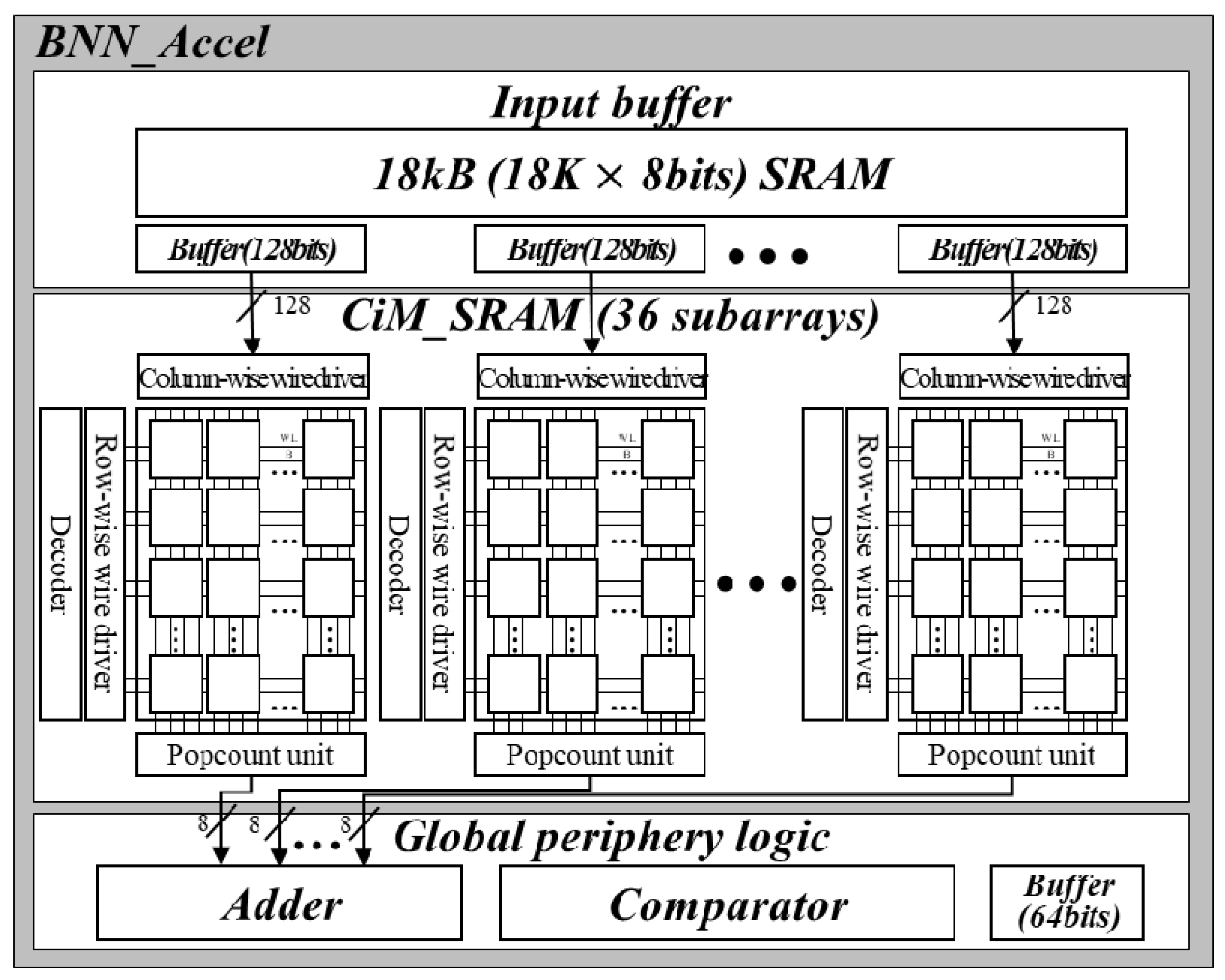
Figure 3 depicts the overall structure of BNN_Accel, which consists of three blocks: an input buffer, CiM_SRAM, and global periphery logic. The input buffer stores the input feature maps (the input data of convolution layers) in 18 kB SRAM and provides the data to CiM_SRAM for the computation. Note 18 kB SRAM is large enough to store the input feature maps of each binarized convolution layer in commonly exploited BNNs (e.g., binarized VGG-16 [5,6,7]). CiM_SRAM is composed of 36 subarrays which store the kernel weights. With the input data provided from the input buffer and kernel weights stored in CiM_SRAM, all the CiM_SRAM subarrays perform XACs in parallel as explained in Section 3.1. Note, before the computations, the input feature maps and kernel weights are prepared in the input buffer and CiM_SRAM, respectively, based on the data mapping scheme which will be explained in Section 3.3. Then, the global periphery logic obtains the final output of the computations in the binarized convolution layer. The adder in the global periphery logic accumulates the partial popcount results from the CiM_SRAM subarrays to obtain the total popcount. The comparator then compares the total popcount with a predefined threshold and stores the final output to the buffer (i.e., when the total popount is less than the threshold, the final output is zero, otherwise, the final output is one). Lastly, the final output in the buffer is sent to the main memory.

3.3. Data Mapping for Parallel Computations in BNN_Accel

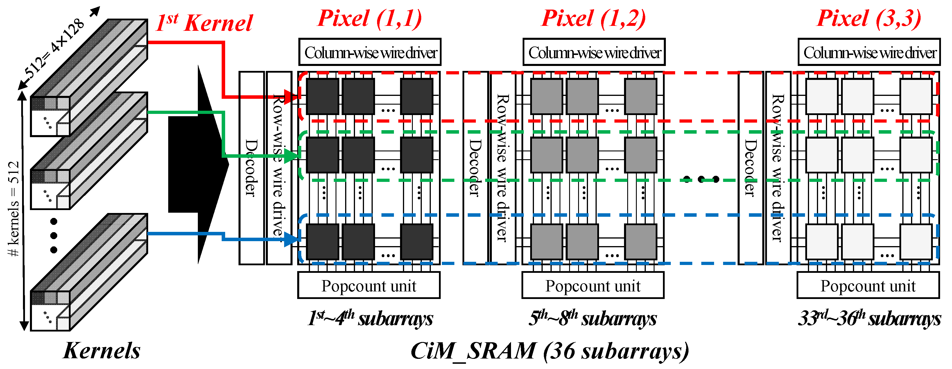
To efficiently perform parallel computations in BNN_Accel, we exploit a data mapping scheme for the input buffer and CiM_SRAM to store the input feature maps and kernel weights, respectively. We map the data for the parallel computation to a single row of a subarray. When the data size is too large to be stored in the single row, we map the rest of the data to a single row of another subarray. In other words, we do not map the data for the parallel computation to multirows of the same subarray. Figure 4 shows the data mapping example for the kernel weights in the 6th convolution layer of binarized VGG-16; there are 512 kernels with the size of 3 × 3 × 512. Note, for each kernel, we simultaneously perform XACs. We map the data on each pixel (512 bits) of the nth kernel to the nth row (128 bits) of four subarrays. For example, we map the data on the pixel (1,1) of the first kernel to the first row of the 1st~4th subarrays, while we map the data on the pixel (1,2) of the first kernel to the first row of the 5th~8th subarrays. In this way, we map all the data on the same kernel to a single row of all the subarrays. Consequently, when all the CiM_SRAM subarrays operate in parallel, XACs for one kernel are performed at the same time.

4. Evaluation

4.1. Evaluation Methodology

We modeled three different CiM_SRAMs with CACTI [11] to evaluate the latency and energy consumption. The size of each CiM_SRAM was 288 kB, since each CiM_SRAM was composed of 36 subarrays with 512-by-128 cell array as explained in Section 3. Note, the latency and energy of the cell were not shown in [9]. We modify CACTI to reflect the additional transistors and wires in CiM_SRAM as follows:
  • We modeled the impact of additional transistors and wires on latency and energy in our modified CACTI, based on the Horowitz equation [11].
  • We modeled the latency and energy of MIVs by adopting the MIV specification from [8].
  • We modeled the area of CiM_SRAMs reflecting the cell structures; CiM_SRAM (M3D_2L) and CiM_SRAM (M3D_4L) had the same cell area as the conventional 6T SRAM, while CiM_SRAM (2D) had 1.5× larger cell area than the 6T SRAM.
In addition, we implemented the Popcount unit with Verilog HDL. Then, we synthesized and placed-and-routed the Popcount unit with the Synopsys Design Compiler [12] and IC Compiler [13]. We exploited the Samsung System LSI 28 nm ASIC library. Meanwhile, since the 28 nm technology node does not exist in CACTI, we modeled CiM_SRAM based on the 22 nm technology node, which is the only sub-30 nm technology node in CACTI.
Table 1 shows the obtained latency and energy of the Popcount unit. Finally, we obtained the latency and energy of CiM_SRAM by adding the results of the Popcount unit to CACTI.
Based on the three CiM_SRAM designs, we evaluated three different BNN_Accels: BNN_Accel (2D), BNN_Accel (M3D_2L), and BNN_Accel (M3D_4L), which were BNN_Accels with CiM_SRAM (2D), CiM_SRAM (M3D_2L), and CiM_SRAM (M3D_4L), respectively. We analyzed the execution time and energy consumption of each BNN_Accel, which executed the computations of each binarized convolution layer in binarized VGG-16 with Cifar-10 dataset [5]; in BNNs, the first convolution layer was not binarized to achieve high network accuracy [1]. We obtained the latency and energy of the input buffer and global periphery logic with the same process as the Popcount unit, as shown in Table 1. Then, we applied the number of cycles and energy taken by each block to gem5-aladdin [14]; BNN_Accel operated at 2.0 GHz.
In M3D integration, there was a concern about the thermal problem induced by high power density and low heat dissipation capability. Thus, we evaluated the peak temperature of each BNN_Accel with HotSpot 6.0 [15]. For a conservative thermal evaluation, each BNN_Accel was placed beside the big CPU core cluster consuming 4.0 W, which was the thermal design power (TDP) of the cluster [16]. Note the big CPU core cluster is the thermal hotspot in mobile SoCs [17]. To reflect the layer material property of M3D integration, we also set the thickness and thermal conductivity of the interlayer dielectric (ILD) to 100.0 nm and 1.4 W/m∙K, respectively [8].

4.2. Evaluation Results

4.2.1. Latency and Energy of CiM_SRAM

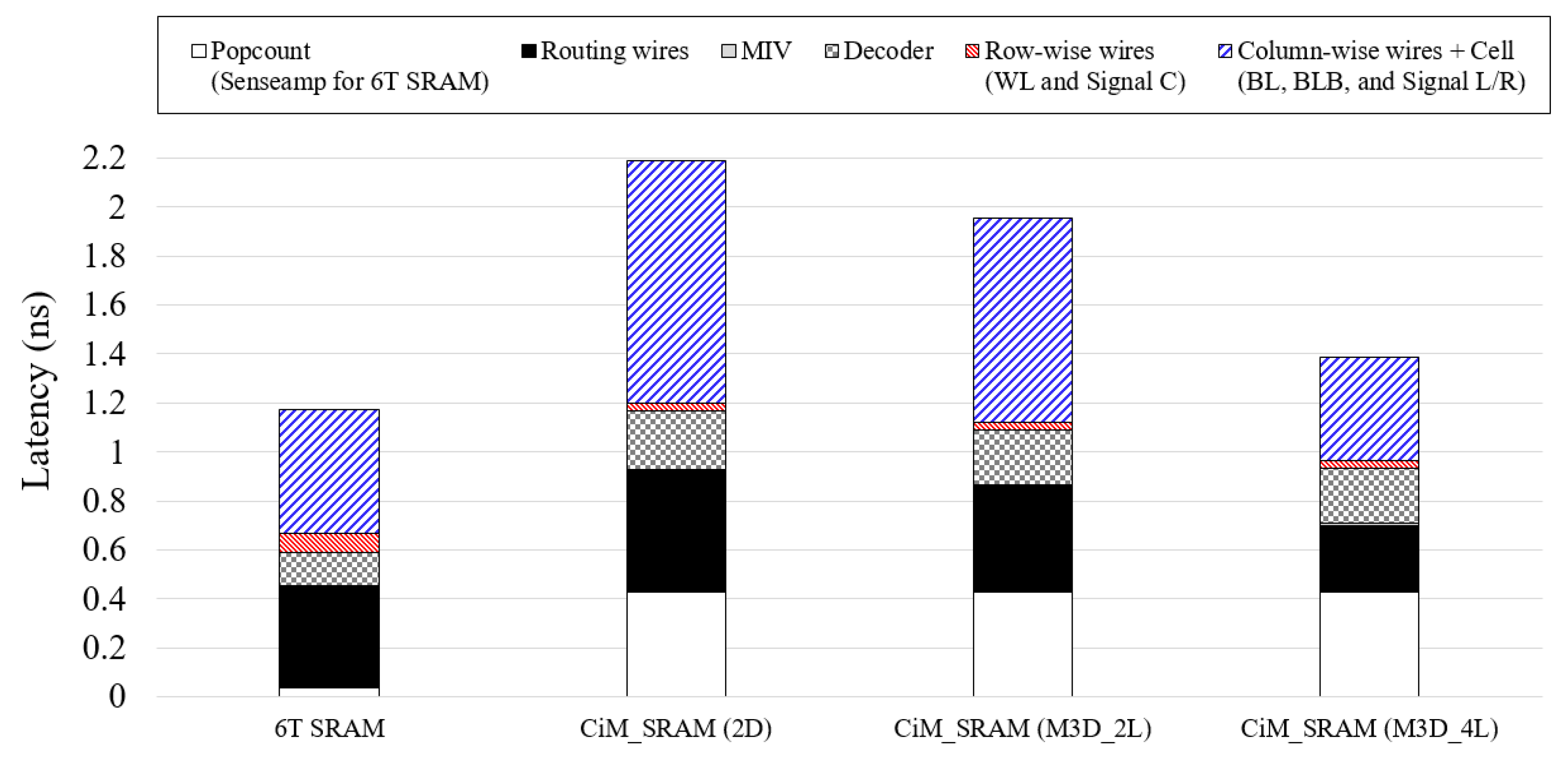
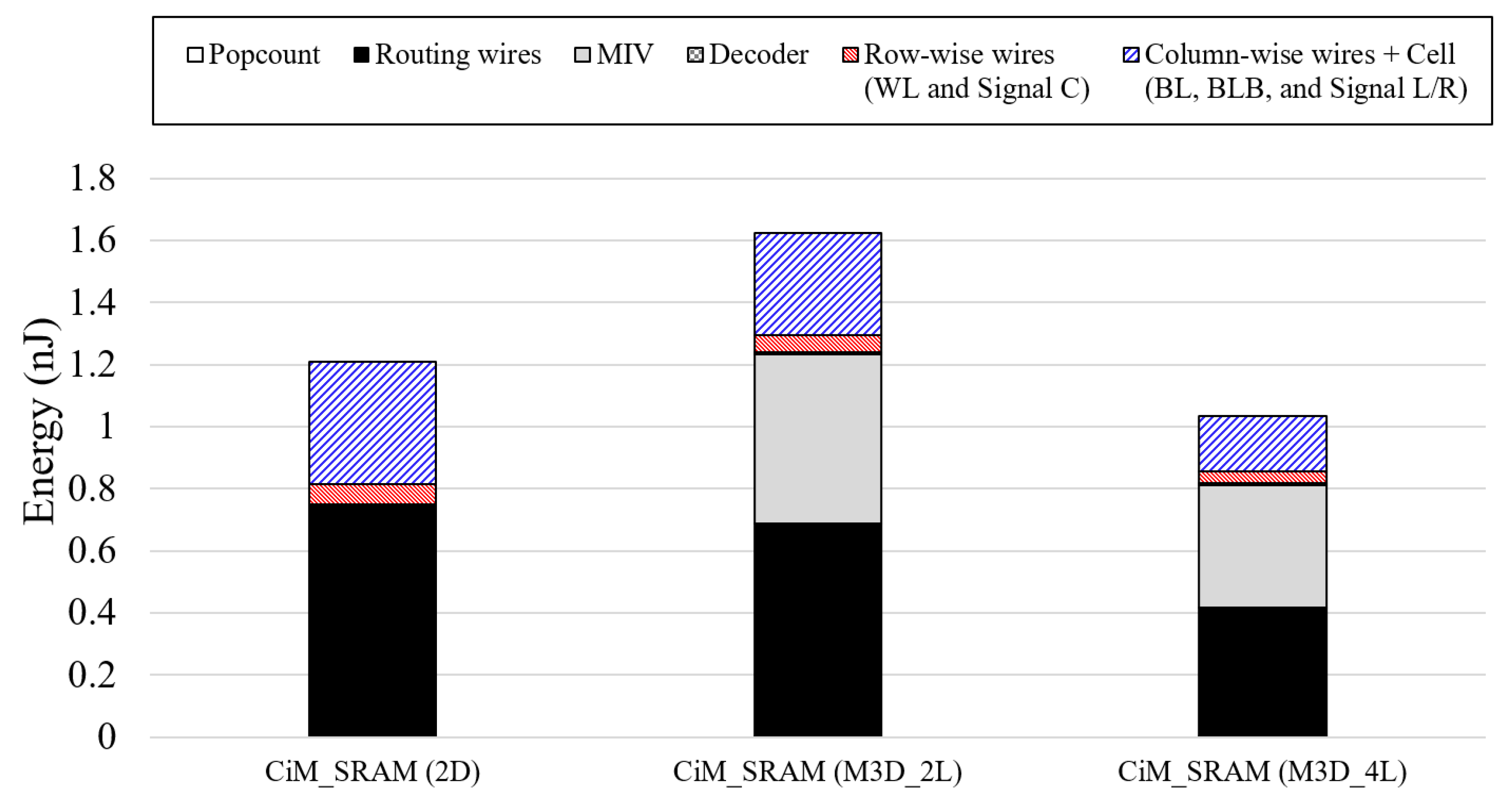
Figure 5 and Figure 6 show the latency and energy consumption of each CiM_SRAM, when it performs XAC; note we present the access (read) latency of the conventional 6T SRAM in Figure 5 for comparison with the XAC latency of CiM_SRAMs. The 6T SRAM has shorter latency than CiM_SRAM (2D), for the following reasons:
  • A read operation in the 6T SRAM uses a smaller number of transistors than an XAC operation in CiM_SRAM (2D), which leads to shorter latency.
  • The 6T SRAM is composed of a smaller number of transistors/wires than CiM_SRAM (2D), which leads to lower parasitic capacitance.
Though CiM_SRAM (2D) required much longer latency for an XAC operation than the read operation in the 6T SRAM, the latency could be reduced significantly by applying M3D BLP design to the CiM_SRAM. As shown in Figure 5, CiM_SRAM (M3D_4L) had 36.6% shorter latency than CiM_SRAM (2D) [9]. CiM_SRAM (M3D_4L) had shorter 2D wires (which included the column-wise wires, row-wise wires, and routing wires between subarrays) than CiM_SRAM (2D), resulting in shorter latency. The reduction of the 2D wire length was due to the following reasons:
  • Thanks to the transistor-level M3D integration, CiM_SRAM (M3D_4L) had 33.8% smaller cell area than CiM_SRAM (2D).
  • CiM_SRAM (M3D_4L) had shorter column-wise wires by adopting the M3D BLP.
  • Thanks to both (1) and (2), CiM_SRAM (M3D_4L) had smaller subarrays, which eventually reduced the length of the routing wires between subarrays.
In addition, CiM_SRAM (M3D_4L) reduced the latency by 10.7% compared to CiM_SRAM (M3D_2L) [9]. Though CiM_SRAM (M3D_4L) had the same cell area as CiM_SRAM (M3D_2L), it led to shorter latencies of the routing wires between subarrays and column-wise wires, due to the M3D BLP; the latencies of CiM_SRAM (2D), CiM_SRAM (M3D_2L), and CiM_SRAM (M3D_4L) were 5 cycles, 4 cycles, and 3 cycles, respectively, at 2.0 GHz (the operating clock frequency of BNN_Accels).
As shown in Figure 6, CiM_SRAM (M3D_4L) consumed 14.0% less energy than CiM_SRAM (2D). The energy reduction also came from shorter 2D wires, thanks to the transistor-level M3D integration and M3D BLP. Though the energy of MIVs (i.e., 3 × 512 × 128 MIVs in the cell array of each subarray) was non-negligible, the amount of energy reduction in 2D wires was higher than the additional MIV energy, attributed to shorter 2D wires. Additionally, CiM_SRAM (M3D_4L) reduced the energy by 36.4% compared to CiM_SRAM (M3D_2L), since it reduced the 2D wire energy thanks to the M3D BLP. Note, though CiM_SRAM (M3D_2L) reduced the 2D wire energy compared to CiM_SRAM (2D), CiM_SRAM (M3D_2L) consumed 34.3% more energy due to the MIV energy.
In Table 2, we summarize the results of CiM_SRAMs in terms of latency, energy, and area, which are normalized to those of CiM_SRAM (2D); note the area indicated 288KB CiM_SRAM area. As described in Table 2, CiM_SRAM (M3D_4L) showed much better latency and energy than CiM_SRAM (2D), with much smaller area, while CiM_SRAM (M3D_2L) showed worse energy efficiency due to its additional MIV energy.

4.2.2. Execution Time and Energy of BNN_Accel

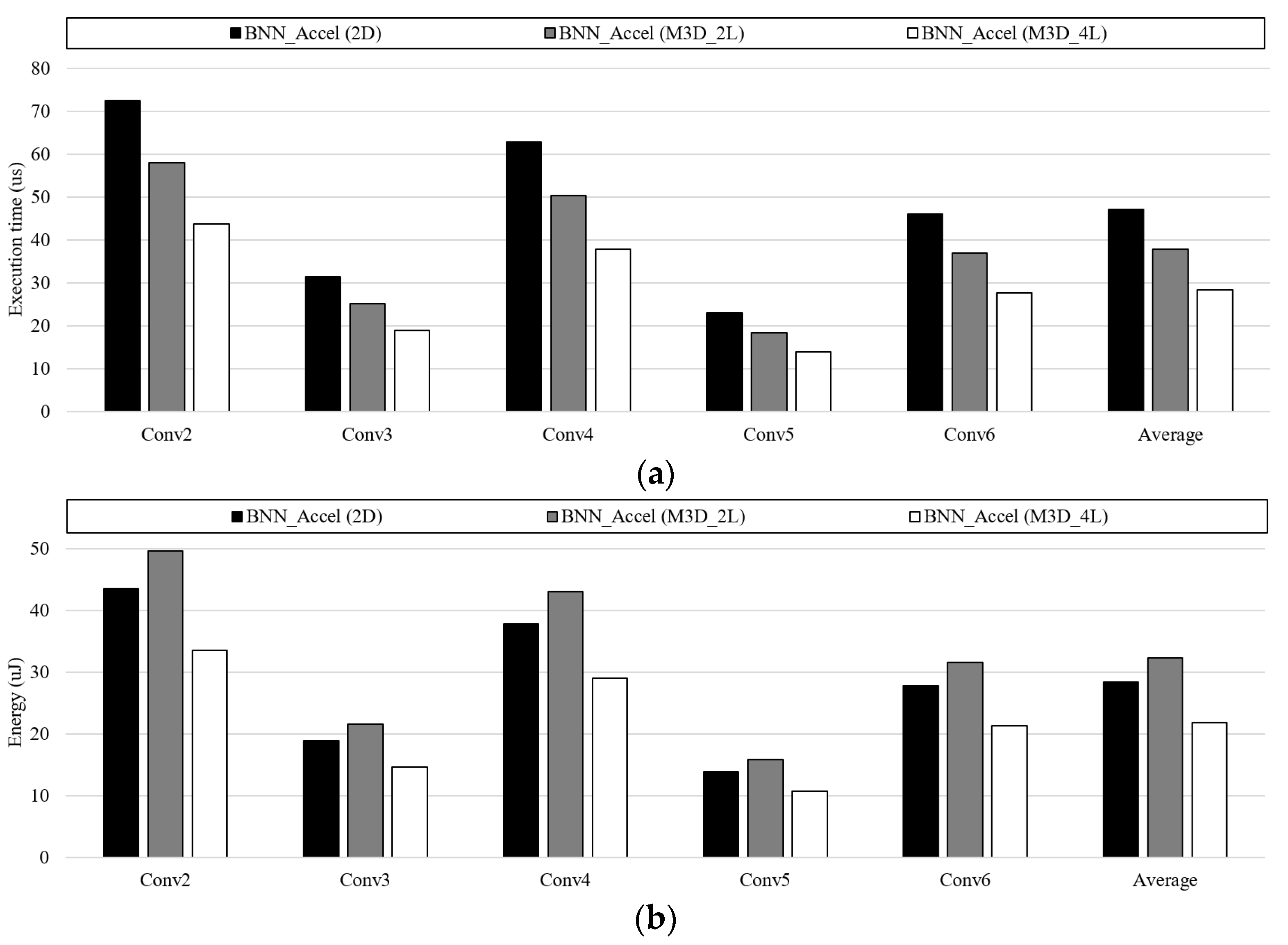
Figure 7 shows the execution time and energy consumption of BNN_Accels, across the binarized convolution layers; note BNN_Accel (2D) is an BNN accelerator based not on 6T SRAM, but on CiM_SRAM (2D). As shown in Figure 7a, BNN_Accel (M3D_4L) had a 39.9% shorter execution time than BNN_Accel (2D), on average. BNN_Accel (M3D_4L) reduced the computation cycles for XAC by 40.0% (2 cycles), compared to BNN_Accel (2D), resulting in shorter execution time. Additionally, BNN_Accel (M3D_4L) reduced the average execution time by 36.4%, compared to BNN_Accel (M3D_2L). The reduction of the execution time also came from the reduced computation cycles for XAC. Note the computations of the binarized convolution layer consisted of many XACs.
As shown in Figure 7b, BNN_Accel (M3D_4L) consumed 23.2% less energy than BNN_Accel (2D), on average. Since BNN_Accel (M3D_4L) reduced the energy for XAC as well as the execution time itself, it reduced the energy compared to BNN_Accel (2D). Thanks to the same reasons, BNN_Accel (M3D_4L) reduced the average energy by 32.5%, compared to BNN_Accel (M3D_2L).
In Table 3, we summarize the results of BNN_Accels in terms of execution time, energy and area, which are normalized to those of BNN_Accel (2D); note the area includes popcount unit, input buffer, and global periphery logic. As described in Table 3, BNN_Accel (M3D_4L) outperformed BNN_Accel (2D), in the perspective of execution time, energy, and area. Since BNN_Accel (M3D_2L) consumed more energy in CiM_SRAM (M3D_2L) (as shown in Figure 6), it resulted in slightly higher energy consumption then BNN_Accel (2D). Consequently, combining transistor-level and subarray-level M3D integration improved performance and energy efficiency, with significant area reduction.

4.2.3. Peak Temperature of BNN_Accel

We analyzed the peak temperature of each BNN_Accel, which was placed beside the thermal hotspot of the mobile SoC. The peak temperatures of BNN_Accel (2D), BNN_Accel (M3D_2L), and BNN_Accel (M3D_4L) were 71.8 ℃, 76.9 ℃, and 79.2 ℃, respectively. Due to the high power density and low heat dissipation capability of M3D integration, the peak temperature of BNN_Accel (M3D_2L) and BNN_Accel (M3D_4L) was higher than that of BNN_Accel (2D). However, the peak temperature was still under the thermal threshold (80.0 ℃ in [18]), which does not invoke the thermal throttling.

4.3. Discussion on Monolithic 3D Fabrication Cost

According to our analysis, M3D_4L is expected to provide much better performance, higher energy efficiency, and even significant area reduction, compared to the conventional 2D design. However, M3D integration is not a mature technology, we need to consider additional fabrication costs compared to the conventional 2D fabrication; for example, some additional design steps are required for stacking multiple layers such as increasing the number of masks. In addition, to prevent damage to the bottom layer, M3D requires low temperature fabrication for each stacked layer, which requires additional equipment for low temperature fabrication (e.g., laser annealing, etc.). To reduce the design costs of M3D fabrication, many researchers have studied M3D across various levels. For example, Or-Bach et al proposed an M3D fabrication method that could be compatible with the conventional 2D process [19]. Additionally, Jiang et al. presented the use of 2D materials for M3D integration [20], which would lead to significant cost reduction in M3D integration, even comparable to 2D ICs. Based on such studies, M3D is already considered to be more cost-effective than the conventional TSV-3D for logic fabrication. Consequently, various studies will enable M3D to be applied to commercial products in the near future.

5. Conclusions

In this paper, we proposed the BNN_Accel for the binarized convolution layers of BNNs, which consisted of CiM_SRAM, input buffer, and global periphery logic. We adopted the subarray-level M3D integration (the M3D BLP) to CiM_SRAM (M3D_4L) for the wire length reduction, which reduced the latency and energy, compared to the CiM_SRAM (2D). Across the binarized convolution layers in a BNN, our system-level evaluation shows that the BNN_Accel (M3D_4L) reduces the average execution time and energy by 39.9% and 23.2%, respectively, compared to BNN_Accel (2D). Though we only showed the results using the binarized VGG-16, our proposed BNN_Accel could provide energy efficiency for more complex networks, by adjusting the size of input buffers and CiM_SRAMs, considering the size of inputs, size of kernels, etc.

Author Contributions

J.H.C.; methodology, data analysis, writing—original draft preparation, Y.-H.G.; data analysis, validation, writing—review and editing, S.W.C.; data analysis, validation, writing—review and editing, supervision. All authors have read and agreed to the published version of the manuscript.

Funding

This work was supported by the National Research Foundation of Korea (NRF) grant funded by the Korea government (MSIT) (No. 2020R1A2C2003500) and funded by the Ministry of Science and ICT for Original Technology Program (No. 2020M3F3A2A01082329). This work also has been conducted by the Research Grant of Kwangwoon University in 2020.

Data Availability Statement

The data presented in this study are available on request from the corresponding author.

Conflicts of Interest

The authors declare no conflict of interest.

References

  1. Gong, Y.-H.; Kong, J.; Chung, S.W. Quantifying the Impact of Monolithic 3D (M3D) Integration on L1 Caches. IEEE Trans. Emerg. Top. Comput. 2019, 1. [Google Scholar] [CrossRef]
  2. Agrawal, A.; Jaiswal, A.; Roy, D.; Han, B.; Srinivasan, G.; Ankit, A.; Roy, K. Xcel-RAM: Accelerating Binary Neural Networks in High-Throughput SRAM Compute Arrays. IEEE Trans. Circuits Syst. I Regul. Pap. 2019, 66, 3064–3076. [Google Scholar] [CrossRef] [Green Version]
  3. Synopsys Design Compiler. Available online: https://www.synopsys.com/implementation-and-signoff/rtl-synthesis-test/design-compiler-graphical.html (accessed on 15 February 2021).
  4. Courbariaux, M.; Hubara, I.; Soudry, D.; El-Yaniv, R.; Bengio, Y. Binarized Neural Networks: Training Deep Neural Networks with Weights and Activations Constrained to +1 or −1. Available online: https://arxiv.org/pdf/1602.02830.pdf (accessed on 17 March 2016).
  5. Jiang, J.; Parto, K.; Cao, W.; Banerjee, K. Monolithic-3D Integration with 2D Materials: Toward Ultimate Vertically-Scaled 3D-ICs. In Proceedings of the 2018 IEEE SOI-3D-Subthreshold Microelectronics Technology Unified Conference (S3S), Burlingame, CA, USA, 15–18 October 2018; pp. 1–3. [Google Scholar]
  6. Jiang, L.; Zhao, B.; Yang, J.; Zhang, Y. Constructing Large and Fast On-Chip Cache for Mobile Processors with Multilevel Cell STT-MRAM Technology. ACM Trans. Des. Autom. Electron. Syst. 2015, 20, 1–24. [Google Scholar] [CrossRef]
  7. Jiang, Z.; Yin, S.; Seo, J.-S.; Seok, M. XNOR-SRAM: In-Bitcell Computing SRAM Macro based on Resistive Computing Mechanism. In Proceedings of the 2019 on Great Lakes Symposium on VLSI, Tysons Corner, VA, USA, 9–11 May 2019; pp. 417–422. [Google Scholar]
  8. Zhang, R.; Stan, M.R.; Skadron, K. Hotspot 6.0: Validation, Acceleration and Extension. Available online: https://www.cs.virginia.edu/~skadron/Papers/HotSpot60_TR.pdf (accessed on 26 August 2015).
  9. Shao, Y.S.; Xi, S.L.; Srinivasan, V.; Wei, G.-Y.; Brooks, D. Co-designing accelerators and SoC interfaces using gem5-Aladdin. In Proceedings of the 49th Annual IEEE/ACM International Symposium on Microarchitecture (MICRO), Taipei, Taiwan, 15–19 October 2016; pp. 1–12. [Google Scholar]
  10. Dey, S.; Guajardo, E.Z.; Basireddy, K.R.; Wang, X.; Singh, A.K.; McDonald-Maier, K. EdgeCoolingMode: An Agent Based Thermal Management Mechanism for DVFS Enabled Heterogeneous MPSoCs. In Proceedings of the 2019 32nd International Conference on VLSI Design and 2019 18th International Conference on Embedded Systems (VLSID), Delhi, India, 5–9 January 2019; pp. 19–24. [Google Scholar]
  11. Synopsys IC Compiler. Available online: https://www.synopsys.com/implementation-and-signoff/physical-implementation/ic-compiler.html (accessed on 15 February 2021).
  12. Kim, Y.G.; Kim, M.; Kong, J.; Chung, S.W. An Adaptive Thermal Management Framework for Heterogeneous Multi-Core Processors. IEEE Trans. Comput. 2020, 69, 894–906. [Google Scholar] [CrossRef]
  13. Hsueh, F.-K.; Chiu, H.-Y.; Shen, C.-H.; Shieh, J.-M.; Tang, Y.-T.; Yang, C.-C.; Chen, H.-C.; Huang, W.-H.; Chen, B.-Y.; Chen, K.-M.; et al. TSV-free FinFET-based Monolithic 3D+-IC with computing-in-memory SRAM cell for intelligent IoT devices. In Proceedings of the 2017 IEEE International Electron Devices Meeting (IEDM), San Francisco, CA, USA, 2–6 December 2017; pp. 12.6.1–12.6.4. [Google Scholar] [CrossRef]
  14. Giacomin, E.; Greenberg-Toledo, T.; Kvatinsky, S.; Gaillardon, P.-E. A Robust Digital RRAM-Based Convolutional Block for Low-Power Image Processing and Learning Applications. IEEE Trans. Circuits Syst. I Regul. Pap. 2018, 66, 643–654. [Google Scholar] [CrossRef]
  15. Yin, S.; Jiang, Z.; Kim, M.; Gupta, T.; Seok, M.; Seo, J.-S. Vesti: Energy-Efficient In-Memory Computing Accelerator for Deep Neural Networks. IEEE Trans. Very Large Scale Integr. (VLSI) Syst. 2019, 28, 48–61. [Google Scholar] [CrossRef]
  16. Mittal, S. A Survey of ReRAM-Based Architectures for Processing-In-Memory and Neural Networks. Mach. Learn. Knowl. Extr. 2019, 1, 75–114. [Google Scholar] [CrossRef] [Green Version]
  17. Li, S.; Chen, K.; Ahn, J.H.; Brockman, J.B.; Jouppi, N.P. CACTI-P: Architecture-level modeling for SRAM-based structures with advanced leakage reduction techniques. In Proceedings of the 2011 IEEE/ACM International Conference on Computer-Aided Design (ICCAD), San Jose, CA, USA, 7–10 November 2011; pp. 694–701. [Google Scholar]
  18. Liu, R.; Peng, X.; Sun, X.; Khwa, W.-S.; Si, X.; Chen, J.-J.; Li, J.-F.; Chang, M.-F.; Yu, S. Parallelizing SRAM Arrays with Customized Bit-Cell for Binary Neural Networks. In Proceedings of the 2018 55th ACM/ESDA/IEEE Design Automation Conference (DAC), San Francisco, CA, USA, 24–28 June 2018; pp. 1–6. [Google Scholar]
  19. Hsueh, F.-K.; Lee, C.-Y.; Xue, C.-X.; Shen, C.-H.; Shieh, J.-M.; Chen, B.-Y.; Chiu, Y.-C.; Chen, H.-C.; Kao, M.-H.; Huang, W.-H.; et al. Monolithic 3D SRAM-CIM Macro Fabricated with BEOL Gate-All-Around MOSFETs. In Proceedings of the 2019 IEEE International Electron Devices Meeting (IEDM), San Francisco, CA, USA, 7–11 December 2019; pp. 3.3.1–3.3.4. [Google Scholar]
  20. Or-Bach, Z.; Cronquist, B.; Wurman, Z.; Beinglass, I.; Henning, A.K. Modified ELTRAN® A game changer for Monolithic 3D. In Proceedings of the 2015 IEEE SOI-3D-Subthreshold Microelectronics Technology Unified Conference (S3S), Rohnert Park, CA, USA, 5–8 October 2015; pp. 1–3. [Google Scholar]
Figure 1. Design and operation procedure of a CiM_SRAM subarray. Note the design of CiM_SRAM subarray is reproduced from [9] and we demonstrate the truth table of XNOR operation in the CiM_SRAM design.
Electronics 10 00623 g001
Figure 2. Three different CiM_SRAM designs. (a) CiM_SRAM (2D); (b) CiM_SRAM (M3D_2L); (c) CiM_SRAM (M3D_4L).
Electronics 10 00623 g002
Figure 3. Overall structure of BNN_Accel.
Electronics 10 00623 g003
Figure 4. An example of data mapping scheme for parallel computations.
Electronics 10 00623 g004
Figure 5. Latency of different SRAM designs (Note the latency value for 6T SRAM represents read latency and those for three different CiM_SRAMs are XAC operation latencies).
Electronics 10 00623 g005
Figure 6. Energy consumption for different CiM_SRAM designs.
Electronics 10 00623 g006
Figure 7. Execution time and energy consumption of three different BNN_Accels across the binarized convolution layers (i.e., Conv) (a) execution time results; (b) energy results.
Electronics 10 00623 g007
Table 1. Implementation Results.
Popcount UnitInput BufferGlobal Periphery Logic
Latency0.43 ns0.28 ns0.64 ns
Dynamic power2.77 mW35.88 mW3.07 mW
Leakage power2.21 µW29.32 µW2.63 µW
Table 2. Normalized results of CiM_SRAMs in terms of latency, energy, and area.
CiM_SRAM (2D)CiM_SRAM (M3D_2L)CiM_SRAM (M3D_4L)
Latency1.0000.893 (10.7% lower)0.634 (36.6% lower)
Energy1.0001.344 (34.4% higher)0.855 (14.5% lower)
Area1.0000.711 (28.9% smaller)0.375 (62.5% smaller)
Table 3. Normalized results of BNN_Accels in terms of execution time, energy and area.
BNN_Accel (2D)BNN_Accel (M3D_2L)BNN_Accel (M3D_4L)
Exec. time1.0000.801 (19.9% faster)0.601 (39.9% faster)
Energy1.0001.133 (13.3% higher)0.768 (23.2% lower)
Area1.0000.759 (24.1% smaller)0.479 (53.1% smaller)
Publisher’s Note: MDPI stays neutral with regard to jurisdictional claims in published maps and institutional affiliations.