1. Introduction
To cater for the demand of high-speed data transfer, various wireless communication technologies have been proposed by researchers. Among those techniques, Long Term Evolution-Advanced (LTE-A) and IEEE 802.11ac are the most widely accepted standards for high volume data exchange. LTE-A can support both downlink and uplink peak data rate over gigabit per second through carrier aggregation (CA), and IEEE 802.11ac can provide approximately 7 Gbps data rate with multi-input-multi-output (MIMO) technology in the unlicensed sub −6 GHz frequency bands. However, millimeter-wave (mm-wave) communication is one of the most promising technologies because of the large available spectrum resource. The mm-wave V-band is allocated at the unlicensed 60 GHz bands ranging from 57 GHz to 71 GHz. The V-band communication is supported by IEEE 802.11ad, which can provide 7 Gbps data transfer without employing CA or MIMO technologies. IEEE 802.11ad supports advanced applications such as instant file transfers, wireless docking, high definition media streaming, coreless computing, and internet access. Furthermore, a recent study on mm-wave communication as part of the fifth generation (5G) communication system has been proven practical [
1].
Transmitter is a key building block of the mm-wave transceiver. The conventional mm-wave transmitter consists of power amplifier, up-converter, and other auxiliary circuits. The power amplifier is the most power-consuming block in the transmitter. Design and implementation of the mm-wave power amplifier in the advanced CMOS technology suffer from various challenges. Traditional power amplifier design using waveform engineering seems to be less effective at mm-wave frequencies due to its low output at the harmonic frequency. Moreover, the output power from an up-converter is normally low in the CMOS process. Therefore, extra drive stage is required to improve the gain of the power amplifier. The drive power required by the up-converter should also be accounted for the efficiency. Therefore, the overall efficiency is quite low for a CMOS mm-wave transmitter. To deal with poor performance of the transmitter in the advanced CMOS technology at mm-wave bands, various techniques such as transistor stacking, distributed power combining, and transmission line matching have been widely used [
2,
3,
4,
5]. However, all of these techniques are area consuming. The injection locking technique has been widely utilized in frequency synthesis circuits, and it can be used for amplification purpose, which alleviates power consumption problem in transmitter design and reduce the production cost.
As for the spectral efficiency and signal noise ratio (SNR), phase-shift keying (PSK) modulation schemes are favored over amplitude shift keying (ASK) and frequency shift keying (FSK) schemes. Moreover, the ON–OFF keying (OOK) modulation often suffers from low output power [
2,
3]. In [
6], a zero-IF 60 GHz transceiver with direct binary phase-shift keying (BPSK) modulation is presented. However, it consumes 374 mW from 1.2 V and 232 mW for a 1.0 V supply. A dual band BPSK transmitter implemented at 60 and 80 GHz is presented in [
7]. The data rates of up to 10 and 8.5 Gbps can be obtained at the low and high bands, respectively. However, the power consumption is 300 mW and the chip is 0.639 mm
2. In this paper, a low power binary phase-shift keying (BPSK) transmitter with small chip area is proposed with injection-locked power amplifier PA.
2. Transmitter Design Considerations
As shown in
Figure 1, the transmitter consists of an up-conversion circuit, gate biased negative trans-conductance core, and output buffer. The up-conversion circuit is made up of a transformer (TF1) and four switching transistors (M1, M2, M3, and M4). The input local oscillator (LO) signal is transformed into differential inputs by transformer TF1. In the conventional Gilbert mixer, an overdrive voltage on the bottom transistor degrades the linearity performance under low supply voltage applications. Therefore, the non-linearity of the bottom transistors may result in LO leakage. Since the injection-locked power amplifier has the highest gain at its resonant frequency, the LO leakage from the up-converter can be minimized. Therefore, the transformer-coupled input is employed in this design.
The geometry of the proposed transformer is shown in
Figure 2. The signal lines of the transformer are located at the top metal layer (Metal 6) and Metal 5, respectively. The bottom metal layer (Metal 1) is used to generate the ground guard ring to minimize the coupling effect.
The gate biased negative conductance (negative-gm) core consists of M5, M6, C1, and C2. In steady-state, the negative conductance generated by the active devices M5 and M6 should equal the loss conductance in the circuit. The gate bias voltage VG are connected to the gates of M5 and M6, which can be used to generate the desired negative-gm. The transformer load TF2, capacitors C1 and C2, and parasitic capacitance of the tank can be used to generate oscillation at the desired frequency. Since the oscillation frequency is susceptible to the output circuits, a buffer stage is employed in this design. Since the most important issues for the millimeter-wave power amplifier is the poor reverse isolation performance, the capacitive cross-coupling neutralization technique is presented in output buffer. The cross-coupled capacitors C3 and C4 are connected between the gate and drain of the opposite-side transistors M7 and M8, respectively. C3 and C4 can cancel the parasitic gate-to-drain capacitance and improve the reverse isolation. The capacitor neutralization technique can improve both reverse isolation performance and gain.
The key parameters of these sub-circuits are listed in
Table 1. The length of all transistors is 65 nm.
The injection-locking behavior can be understood as the synchronization process between a high output power oscillator and its input signal. The synchronization is dependent on the design parameters of the oscillator, and the frequency difference between the injected controlling signal and the free running frequency of the oscillator.
The proposed injection-locking transmitter (ILTX) in this paper is expected to translate at a data rate of 2.25 Gbps with an output power of around 10 dBm, and the power consumption is larger than 70 mW.
3. Results and Discussion
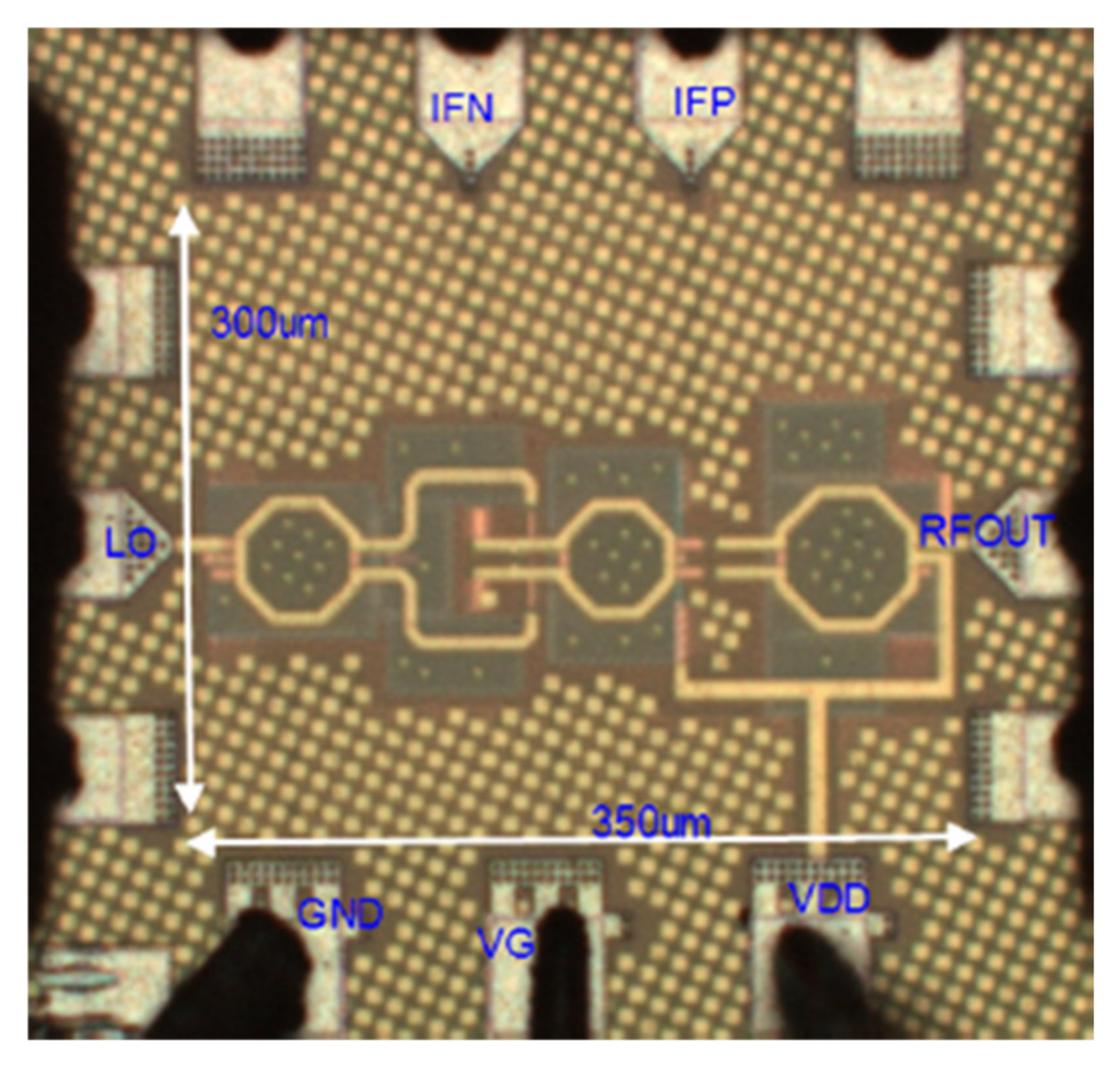
A BPSK ILTX was fabricated in Global Foundries 65 nm CMOS low power technology with a core area of 300 × 350 μm. A circuit photograph is shown in
Figure 3. The LO and RF signal are connected to ground-signal-ground (GSG) pads, and the IF signal from an external waveform generator is provided through ground-signal-signal-ground (GSSG) pads. Since the best performance of ILTX occurs when the injection frequency is equal to the self-running frequency, a large signal measurement was employed to evaluate the output power and efficiency. The large signal test is initially conducted when the IF signal is DC biased to measure its free-running frequency.
The measurement results are depicted in
Figure 4. An output power range from −1.5 dBm to 10.2 dBm was achieved when the bias voltage is tuned from 0.6 V to 1 V. Therefore, the ILTX is able to support various power modes without changing its supply voltage, which typically requires extra power management circuit. The corresponding efficiency varies from 1.5% to 10.1%. The simulated results show a maximum output power over 12.4 dBm, while the highest efficiency is over 18% with the same current. Considering the accuracy of the large signal model, the discrepancies are within our expectation.
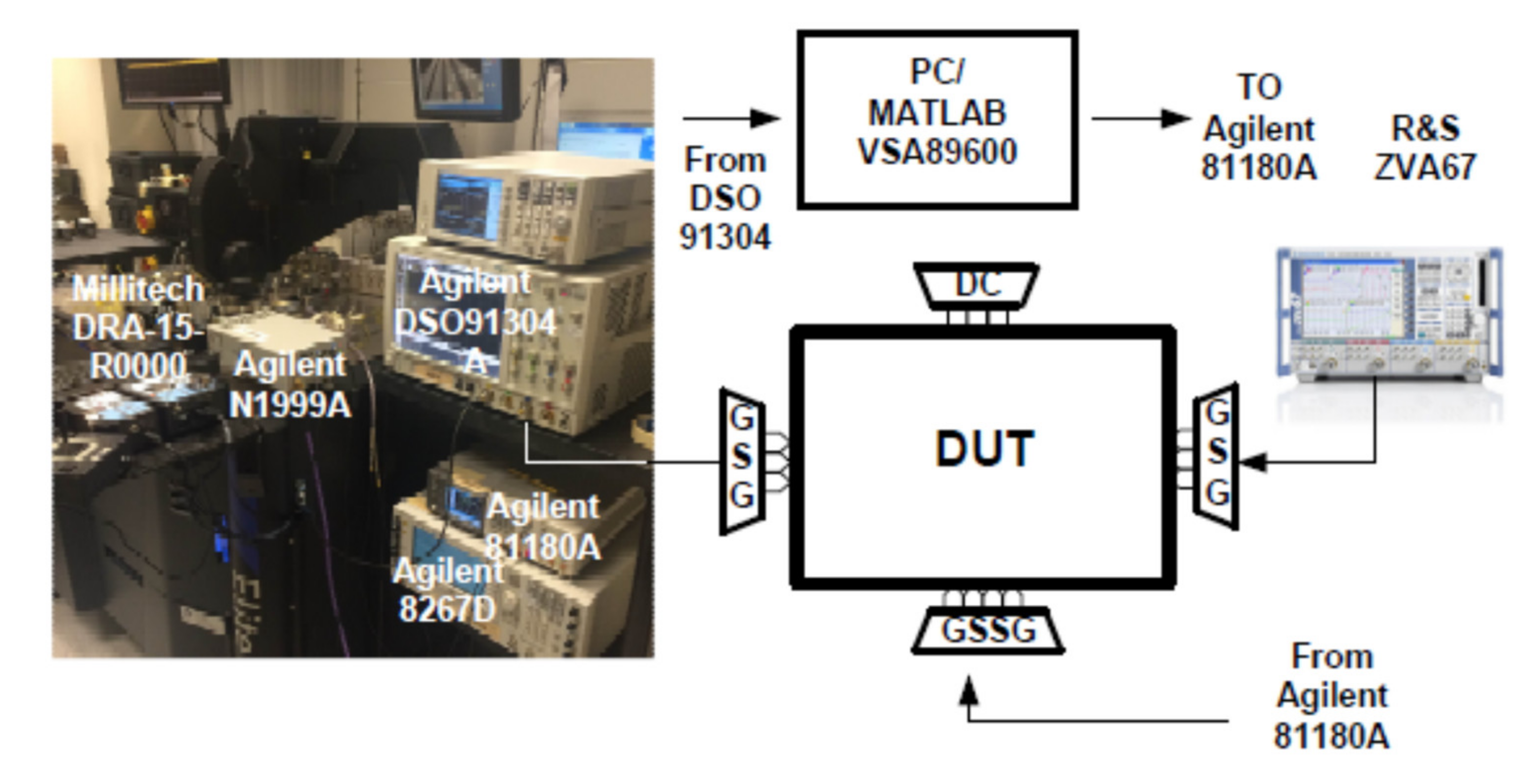
The error vector magnitude (EVM) is a measurement to quantify the performance of the circuit by taking into account all the non-linearities in the transmit and receive chain. As for the injection locking process, the main non-linearity source is the transient phase that lags between its input and output. The EVM measurement setup is shown in
Figure 5. Firstly, the BPSK modulation signal can be generated from MATLAB and downloaded into the Agilent 81180A Arbitrary Waveform Generator (AWG) with a sampling rate of 4 Gbps. A 55 GHz LO signal is generated by R&S ZVA67 (R&S, Munich, Germany). The output of ILTX is initially attenuated by the Millitech DRA −15 attenuator to −20 dBm as required by the Agilent N1999A harmonic mixer. The N1999AX4 harmonic mixer is supplied with 15 GHz signal from ESG8267D for the down-conversion purpose. Therefore, the output of ILTX will be down converted into the 5 GHz frequency band. The Agilent DSO91304A oscillator scope with sampling rate up to 40 Gbps was employed to sample the down converted output. The sampled signals were analyzed by VSA89600 software.
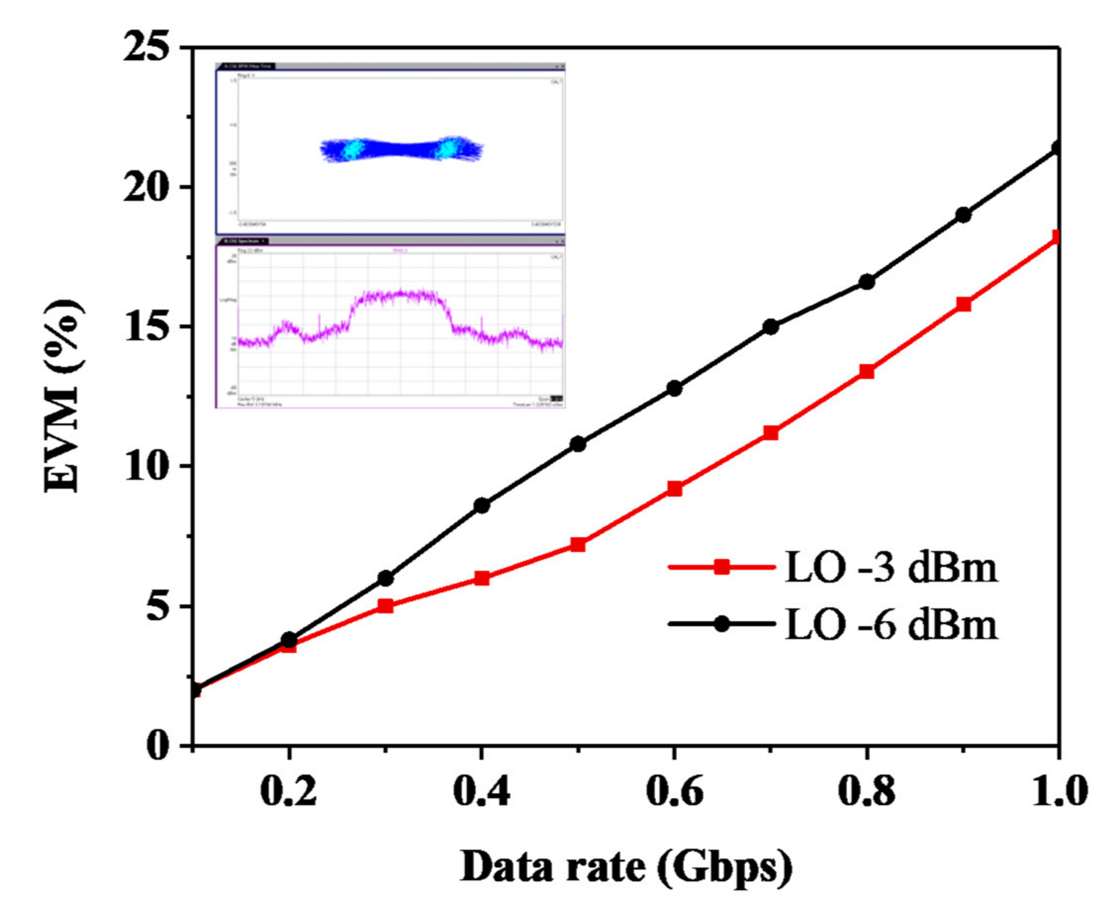
The measured EVM performance is shown in
Figure 6. When the LO input level is −3 dBm, the data rate is 0.2 Gbps and the EVM error is less than 5%. When the LO input level is −6 dBm, the data rate is 1 Gbps and the EVM error is less than 20%. The EVM error slightly reduces at a high data rate range (about 0.2 Gbps) when the LO input level increases from −6 dBm to −3 dBm, which agrees with previous analysis. The BPSK constellation and output spectrum of 1 Gbps are shown at the upper left of
Figure 6.
A comparison table of the mm-wave CMOS transmitter is shown in
Table 2. The injection-locked transmitter has its advantages over the conventional transmitter since it utilized a positive-feedback amplification stage, thus is capable of achieving high gain with low power consumption. However, the drawback is the trade-off between gain and bandwidth. As we can see from the comparison table, [
2,
3,
4,
5,
6,
7,
8,
9] demonstrates much larger bandwidths compared to our work. Although [
6,
7] demonstrates the fastest BPSK transmission, the power consumption is over 300 mw and the output power level is below 10 dBm, and the power consumption of the LO driver is much higher than this work, which operates with a LO level less than −3 dBm. With the increase of the modulation speed, the phase error between input signal and output signal also increases, thus leading to the degradation of EVM. Nevertheless, the injection-locked transmitter demonstrates much better linearity on the spectrum compared to OOK types and much higher efficiency than other linear type transmitters. In summary, the injection-locked BPSK transmitter is suitable for application in uplink transmission where efficiency and output power level are high priority.
4. Conclusions
The proposed injection-locked BPSK transmitter is fabricated in a Global Foundries 65 nm CMOS process occupying a die area of 0.105 mm2. The measurement results show the presented V-band ILTX achieves a data rate over 1 Gbps with EVM less than 20%, and the output power of 10.2 dBm and efficiency over 10% with a minimum required LO power level as low as −6 dBm. The demonstrated ILTX is a compact design, while delivering comparable performance. Therefore, the proposed ILTX is suitable for handset applications.
Author Contributions
Conceptualization, J.L.; methodology, J.L. and G.L.; investigation, H.P.; Formal analysis, Q.Y.; measurement, J.L.; writing—original draft preparation, J.L. and H.P.; writing—review and editing, R.B. and G.L.; supervision and funding acquisition, G.L. All authors have read and agreed to the published version of the manuscript.
Funding
This work was funded in part by the National Natural Science Foundation of China under Grant No. 61671330 and No. 61340049, the Science and Technology Department of Zhejiang Province under Grant No. LGG19F010009, and Wenzhou City Key Science and Technology Innovation Team Program under Grant No. C20170005.
Institutional Review Board Statement
Not applicable.
Informed Consent Statement
Not applicable.
Data Availability Statement
The data supporting this research article are available upon request to the corresponding author.
Conflicts of Interest
The authors declare no conflict of interest.
References
- Sahoo, B.P.S.; Chou, C.; Weng, C.; Wei, H. Enabling millimeter-wave 5G networks for massive IoT applications: A closer look at the issues impacting millimeter-waves in consumer devices under the 5G framework. IEEE Consum. Electron. Mag. 2019, 8, 49–54. [Google Scholar] [CrossRef]
- Byeon, C.W.; Park, C.S. A high-efficiency 60-GHz CMOS transmitter for short-range wireless communications. IEEE Microw. Wireless Compon. Lett. 2017, 27, 751–753. [Google Scholar] [CrossRef]
- Meng, X.; Chi, B.; Wang, Z. A 152-GHz OOK transmitter with 3-dBm output power in 65-nm CMOS. IEEE Microw. Wireless Compon. Lett. 2017, 27, 748–750. [Google Scholar] [CrossRef]
- Lee, C.J.; Kim, S.H.; Son, H.S.; Kang, D.M.; Kim, J.H.; Byeon, C.W.; Park, C.S. A 120 GHz I/Q transmitter front-end in a 40 nm CMOS for wireless chip to chip communication. In Proceedings of the 2018 IEEE Radio Frequency Integrated Circuits Symposium (RFIC), Philadelphia, PA, USA, 10–12 June 2018; pp. 192–195. [Google Scholar]
- Ma, S.; Wu, T.; Zhang, J. A 151-to-173 GHz FMCW transmitter achieving 14 dBm Psat with synchronized injection-locked power amplifiers and five in-phase power combining doublers in 65nm CMOS. In Proceedings of the 2018 IEEE Radio Frequency Integrated Circuits Symposium (RFIC), Philadelphia, PA, USA, 10–12 June 2018; pp. 268–271. [Google Scholar]
- Tomkins, A.; Aroca, R.A.; Yamamoto, T.; Nicolson, S.T.; Doi, Y.; Voinigescu, S.P. A Zero-IF 60 GHz 65 nm CMOS Transceiver With Direct BPSK Modulation Demonstrating up to 6 Gb/s Data Rates Over a 2 m Wireless Link. IEEE J. Solid-State Circuits 2009, 44, 2085–2099. [Google Scholar] [CrossRef]
- Rubin, A.; Socher, E. Dual band 18.5 Gbps transmitter at 60 GHz and 80 GHz in 65nm CMOS. In Proceedings of the 2013 European Microwave Integrated Circuit Conference, Nuremberg, Germany, 6–8 October 2013; pp. 77–80. [Google Scholar]
- Indirayanti, P.; Ayhan, T.; Verhelst, M.; Dehaene, W.; Reynaert, P. A mm-Precise 60 GHz Transmitter in 40 nm CMOS for Discrete-Carrier Indoor Localization. IEEE J. Solid-State Circuits 2015, 50, 1604–1617. [Google Scholar] [CrossRef]
- Kim, C.Y.; Hong, S. A 254 GHz CMOS transmitter with VCO-Q modulation. IEEE Microw. Wireless Compon. Lett. 2016, 26, 458–460. [Google Scholar]
- Kuo, N.; Niknejad, A.M. An E-band QPSK transmitter element in 28-nm CMOS with multistate power amplifier for digitally-modulated phased arrays. In Proceedings of the 2018 IEEE Radio Frequency Integrated Circuits Symposium (RFIC), Philadelphia, PA, USA, 10–12 June 2018; pp. 184–187. [Google Scholar]
- Zhong, Q.; Chen, Z.; Sharma, N.; Kshattry, S.; Choi, W.; Kenneth, K.O. 300-GHz CMOS QPSK transmitter for 30-Gbps dielectric waveguide communication. In Proceedings of the 2018 IEEE Custom Integrated Circuits Conference (CICC), San Diego, CA, USA, 8–11 April 2018; pp. 268–271. [Google Scholar]
| Publisher’s Note: MDPI stays neutral with regard to jurisdictional claims in published maps and institutional affiliations. |
© 2021 by the authors. Licensee MDPI, Basel, Switzerland. This article is an open access article distributed under the terms and conditions of the Creative Commons Attribution (CC BY) license (http://creativecommons.org/licenses/by/4.0/).


