
A 2.53 NEF 8-bit 10 kS/s 0.5 μm CMOS Neural Recording Read-Out Circuit with High Linearity for Neuromodulation Implants


Abstract
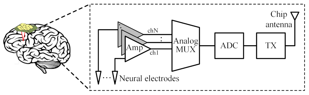
1. Introduction
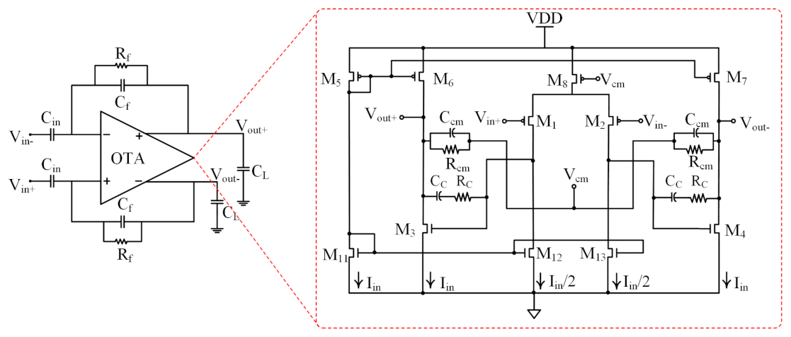
2. Amplifier Architecture
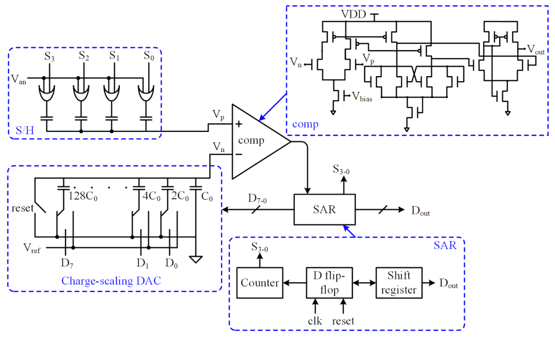
3. ADC Architecture
3.1. Charge-Scaling DAC
3.2. Comparator
4. Measurement Results and Discussion
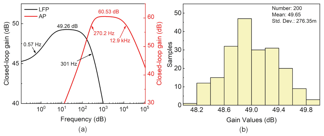
4.1. Amplifier Characterization
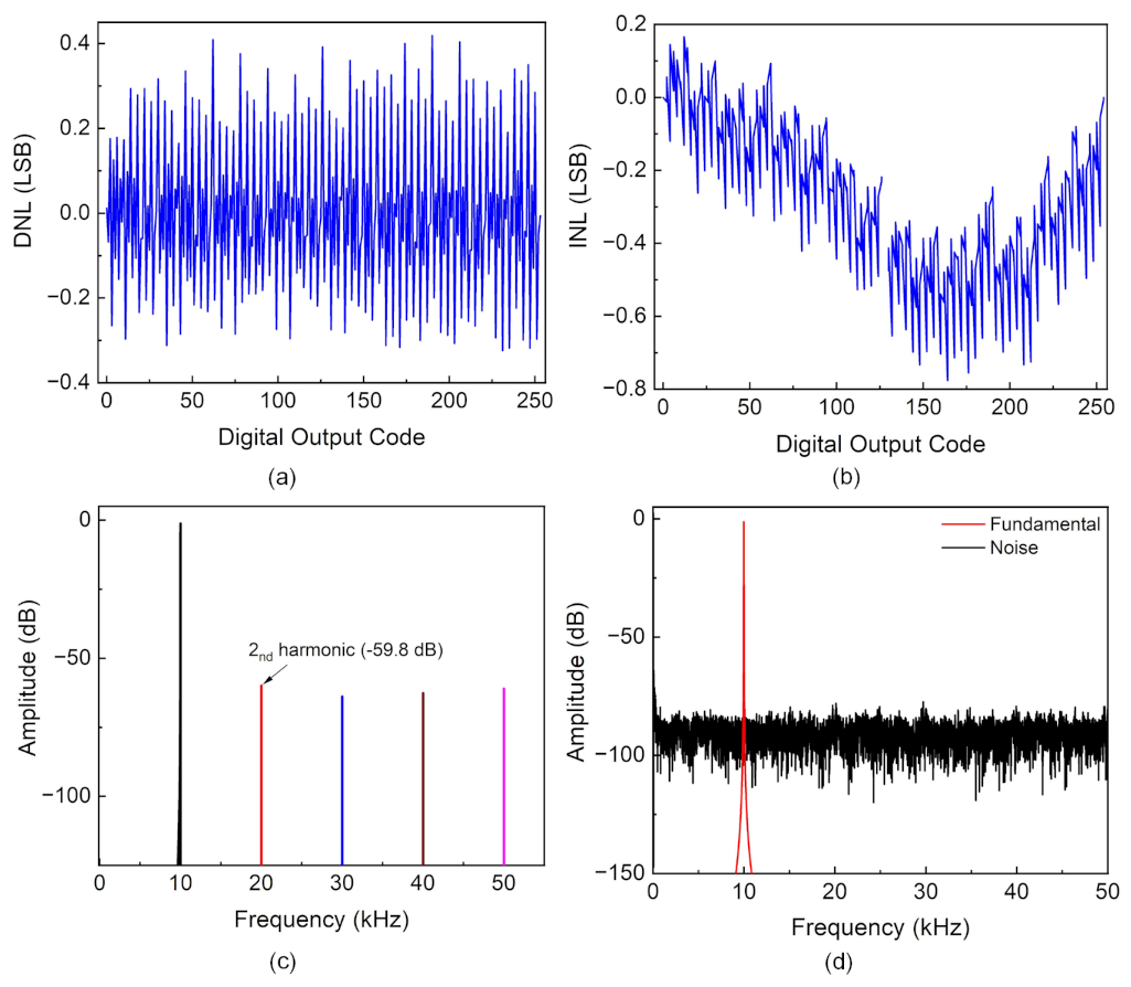
4.2. ADC Characterization
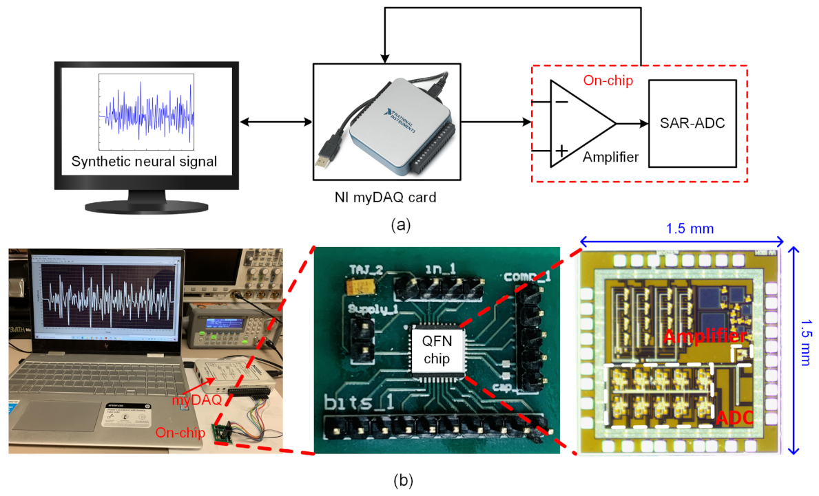
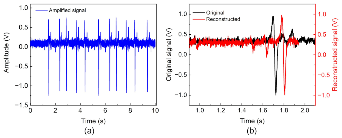
4.3. Neural Signal Amplification and Digitization
5. Conclusions
Author Contributions
Funding
Data Availability Statement
Conflicts of Interest
References
- Zou, X.; Liu, L.; Cheong, J.H.; Yao, L.; Li, P.; Cheng, M.Y.; Goh, W.L.; Rajkumar, R.; Dawe, G.S.; Cheng, K.W.; et al. A 100-channel 1-mW implantable neural recording IC. IEEE Trans. Circuits Syst. I Regul. Pap. 2013, 60, 2584–2596. [Google Scholar] [CrossRef]
- Lee, S.B.; Lee, B.; Kiani, M.; Mahmoudi, B.; Gross, R.; Ghovanloo, M. An inductively-powered wireless neural recording system with a charge sampling analog front-end. IEEE Sens. J. 2015, 16, 475–484. [Google Scholar] [CrossRef]
- Jia, Y.; Guler, U.; Lai, Y.P.; Gong, Y.; Weber, A.; Li, W.; Ghovanloo, M. A trimodal wireless implantable neural interface system-on-chip. IEEE Trans. Biomed. Circuits Syst. 2020. [Google Scholar] [CrossRef]
- Yang, K.W.; Oh, K.; Ha, S. Challenges in scaling down of free-floating implantable neural interfaces to millimeter scale. IEEE Access 2020, 8, 133295–133320. [Google Scholar] [CrossRef]
- Zhou, A.; Santacruz, S.R.; Johnson, B.C.; Alexandrov, G.; Moin, A.; Burghardt, F.L.; Rabaey, J.M.; Carmena, J.M.; Muller, R. A wireless and artefact-free 128-channel neuromodulation device for closed-loop stimulation and recording in non-human primates. Nat. Biomed. Eng. 2019, 3, 15–26. [Google Scholar] [CrossRef] [PubMed]
- Borton, D.A.; Yin, M.; Aceros, J.; Nurmikko, A. An implantable wireless neural interface for recording cortical circuit dynamics in moving primates. J. Neural Eng. 2013, 10, 026010. [Google Scholar] [CrossRef] [PubMed]
- Ando, H.; Takizawa, K.; Yoshida, T.; Matsushita, K.; Hirata, M.; Suzuki, T. Wireless multichannel neural recording with a 128-Mbps UWB transmitter for an implantable brain-machine interfaces. IEEE Trans. Biomed. Circuits Syst. 2016, 10, 1068–1078. [Google Scholar] [CrossRef]
- Tasneem, N.; Mahbub, I. A low-power reconfigurable readout circuit with large DC offset reduction for neural signal recording applications. In Proceedings of the 2020 IEEE 63rd International Midwest Symposium on Circuits and Systems (MWSCAS), Springfield, MA, USA, 9–12 August 2020; pp. 521–524. [Google Scholar]
- Kwak, J.Y.; Park, S.Y. Compact Continuous Time Common-Mode Feedback Circuit for Low-Power, Area-Constrained Neural Recording Amplifiers. Electronics 2021, 10, 145. [Google Scholar] [CrossRef]
- Lee, S.B.; Lee, H.M.; Kiani, M.; Jow, U.M.; Ghovanloo, M. An inductively powered scalable 32-channel wireless neural recording system-on-a-chip for neuroscience applications. IEEE Trans. Biomed. Circuits Syst. 2010, 4, 360–371. [Google Scholar]
- Kim, S.; Na, S.I.; Yang, Y.; Kim, H.; Kim, T.; Cho, J.S.; Kim, J.; Chang, J.W.; Kim, S. A 4× 32-channel neural recording system for deep brain stimulation systems. J. Semicond. Technol. Sci. 2017, 17, 129–140. [Google Scholar] [CrossRef]
- Wattanapanitch, W.; Sarpeshkar, R. A low-power 32-channel digitally programmable neural recording integrated circuit. IEEE Trans. Biomed. Circuits Syst. 2011, 5, 592–602. [Google Scholar] [CrossRef]
- Szuts, T.A.; Fadeyev, V.; Kachiguine, S.; Sher, A.; Grivich, M.V.; Agrochão, M.; Hottowy, P.; Dabrowski, W.; Lubenov, E.V.; Siapas, A.G.; et al. A wireless multi-channel neural amplifier for freely moving animals. Nat. Neurosci. 2011, 14, 263. [Google Scholar] [CrossRef]
- Gosselin, B.; Ayoub, A.E.; Roy, J.F.; Sawan, M.; Lepore, F.; Chaudhuri, A.; Guitton, D. A mixed-signal multichip neural recording interface with bandwidth reduction. IEEE Trans. Biomed. Circuits Syst. 2009, 3, 129–141. [Google Scholar] [CrossRef]
- Bagheri, A.; Salam, M.T.; Velazquez, J.L.P.; Genov, R. Low-frequency noise and offset rejection in DC-coupled neural amplifiers: A review and digitally-assisted design tutorial. IEEE Trans. Biomed. Circuits Syst. 2016, 11, 161–176. [Google Scholar] [CrossRef]
- Hashemi Noshahr, F.; Nabavi, M.; Sawan, M. Multi-channel neural recording implants: A review. Sensors 2020, 20, 904. [Google Scholar] [CrossRef]
- Liu, Z.; Tang, J.; Gao, B.; Li, X.; Yao, P.; Lin, Y.; Liu, D.; Hong, B.; Qian, H.; Wu, H. Multichannel parallel processing of neural signals in memristor arrays. Sci. Adv. 2020, 6, eabc4797. [Google Scholar] [CrossRef]
- Yin, M.; Ghovanloo, M. Using pulse width modulation for wireless transmission of neural signals in multichannel neural recording systems. IEEE Trans. Neural Syst. Rehabil. Eng. 2009, 17, 354–363. [Google Scholar]
- Chowdhury, M.H.; Elyahoodayan, S.; Song, D.; Cheung, R.C. An FPGA-Based Neuron Activity Extraction Unit for a Wireless Neural Interface. Electronics 2020, 9, 1834. [Google Scholar] [CrossRef]
- Shon, A.; Chu, J.U.; Jung, J.; Kim, H.; Youn, I. An implantable wireless neural interface system for simultaneous recording and stimulation of peripheral nerve with a single cuff electrode. Sensors 2018, 18, 1. [Google Scholar] [CrossRef]
- Lee, J.H.; Kim, H.; Kim, J.H.; Lee, S.H. Soft implantable microelectrodes for future medicine: Prosthetics, neural signal recording and neuromodulation. Lab A Chip 2016, 16, 959–976. [Google Scholar] [CrossRef]
- Ng, K.A.; Greenwald, E.; Xu, Y.P.; Thakor, N.V. Implantable neurotechnologies: A review of integrated circuit neural amplifiers. Med. Biol. Eng. Comput. 2016, 54, 45–62. [Google Scholar] [CrossRef]
- Das, R.; Moradi, F.; Heidari, H. Biointegrated and wirelessly powered implantable brain devices: A review. IEEE Trans. Biomed. Circuits Syst. 2020, 14, 343–358. [Google Scholar] [CrossRef]
- Gosselin, B. Recent advances in neural recording microsystems. Sensors 2011, 11, 4572–4597. [Google Scholar] [CrossRef]
- Lin, Q.; Song, S.; Castro, I.D.; Jiang, H.; Konijnenburg, M.; van Wegberg, R.; Biswas, D.; Stanzione, S.; Sijbers, W.; Van Hoof, C.; et al. Wearable Multiple Modality Bio-Signal Recording and Processing on Chip: A Review. IEEE Sens. J. 2020, 21, 1108–1123. [Google Scholar] [CrossRef]
- Liu, Y.; Zhou, Z.; Zhou, Y.; Li, W.; Wang, Z. A Low-Noise Chopper Amplifier with Offset and Low-Frequency Noise Compensation DC Servo Loop. Electronics 2020, 9, 1797. [Google Scholar] [CrossRef]
- Pazhouhandeh, M.R.; Kassiri, H.; Shoukry, A.; Weisspapir, I.; Carlen, P.L.; Genov, R. Opamp-Less Sub-μW/Channel Δ-Modulated Neural-ADC With Super-GΩ Input Impedance. IEEE J. Solid-State Circuits 2020. [Google Scholar] [CrossRef]
- Tran, L.; Cha, H.K. An ultra-low-power neural signal acquisition analog front-end IC. Microelectron. J. 2021, 107, 104950. [Google Scholar] [CrossRef]
- Chandrakumar, H.; Marković, D. A high dynamic-range neural recording chopper amplifier for simultaneous neural recording and stimulation. IEEE J. Solid-State Circuits 2017, 52, 645–656. [Google Scholar] [CrossRef]
- Tasneem, N.T.; Mahbub, I. Design of a 52.5 dB neural amplifier with noise-power trade-off. In Proceedings of the 2019 IEEE 62nd International Midwest Symposium on Circuits and Systems (MWSCAS), Dallas, TX, USA, 4–7 August 2019; pp. 921–924. [Google Scholar]
- Majidzadeh, V.; Schmid, A.; Leblebici, Y. Energy efficient low-noise neural recording amplifier with enhanced noise efficiency factor. IEEE Trans. Biomed. Circuits Syst. 2011, 5, 262–271. [Google Scholar] [CrossRef]
- Kmon, P.; Gryboś, P. Energy efficient low-noise multichannel neural amplifier in submicron CMOS process. IEEE Trans. Circuits Syst. I Regul. Pap. 2013, 60, 1764–1775. [Google Scholar] [CrossRef]
- Valtierra, J.L.; Delgado-Restituto, M.; Fiorelli, R.; Rodríguez-Vázquez, Á. A Sub-μW Reconfigurable Front-End for Invasive Neural Recording That Exploits the Spectral Characteristics of the Wideband Neural Signal. IEEE Trans. Circuits Syst. I Regul. Pap. 2020, 67, 1426–1437. [Google Scholar] [CrossRef]
- Yang, T.; Holleman, J. An ultralow-power low-noise CMOS biopotential amplifier for neural recording. IEEE Trans. Circuits Syst. II Express Briefs 2015, 62, 927–931. [Google Scholar] [CrossRef]
- Maghami, M.H.; Sodagar, A.M. Compact, programmable, two-Stage configuration for implantable biopotential recording amplifiers. J. Circuits Syst. Comput. 2019, 28, 1920009. [Google Scholar] [CrossRef]
- Saidulu, B.; Manoharan, A. Power and area efficient opamp for biomedical applications using 20 nm-TFET. In Microelectronics, Electromagnetics and Telecommunications; Springer: Berlin/Heidelberg, Germany, 2018; pp. 207–215. [Google Scholar]
- Zhang, J.; Zhang, H.; Sun, Q.; Zhang, R. A low-noise, low-power amplifier with current-reused OTA for ECG recordings. IEEE Trans. Biomed. Circuits Syst. 2018, 12, 700–708. [Google Scholar] [CrossRef]
- Rezaei, M.; Maghsoudloo, E.; Bories, C.; De Koninck, Y.; Gosselin, B. A low-power current-reuse analog front-end for high-density neural recording implants. IEEE Trans. Biomed. Circuits Syst. 2018, 12, 271–280. [Google Scholar] [CrossRef] [PubMed]
- Qian, C.; Parramon, J.; Sanchez-Sinencio, E. A micropower low-noise neural recording front-end circuit for epileptic seizure detection. IEEE J. Solid-State Circuits 2011, 46, 1392–1405. [Google Scholar] [CrossRef]
- Shahrokhi, F.; Abdelhalim, K.; Serletis, D.; Carlen, P.L.; Genov, R. The 128-channel fully differential digital integrated neural recording and stimulation interface. IEEE Trans. Biomed. Circuits Syst. 2010, 4, 149–161. [Google Scholar] [CrossRef]
- Wang, J.; Hua, Y.; Zhu, Z. A 10-bit reconfigurable ADC with SAR/SS mode for neural recording. Analog. Integr. Circuits Signal Process 2019, 101, 297–305. [Google Scholar] [CrossRef]
- Lee, J.; Rhew, H.G.; Kipke, D.R.; Flynn, M.P. A 64 channel programmable closed-loop neurostimulator with 8 channel neural amplifier and logarithmic ADC. IEEE J. Solid-State Circuits 2010, 45, 1935–1945. [Google Scholar] [CrossRef]
- Barati, S.; Yavari, M. An adaptive continuous-time incremental ΣΔ ADC for neural recording implants. Int. J. Circuit Theory Appl. 2019, 47, 187–203. [Google Scholar] [CrossRef]
- Qian, C.; Shi, J.; Parramon, J.; Sánchez-Sinencio, E. A low-power configurable neural recording system for epileptic seizure detection. IEEE Trans. Biomed. Circuits Syst. 2013, 7, 499–512. [Google Scholar] [CrossRef]
- Shulyzki, R.; Abdelhalim, K.; Bagheri, A.; Florez, C.M.; Carlen, P.L.; Genov, R. 256-site active neural probe and 64-channel responsive cortical stimulator. In Proceedings of the 2011 IEEE Custom Integrated Circuits Conference (CICC), San Jose, CA, USA, 19–21 September 2011; pp. 1–4. [Google Scholar] [CrossRef]
- Lu, T.C.; Van, L.D.; Lin, C.S.; Huang, C.M. A 0.5 V 1KS/s 2.5 nW 8.52-ENOB 6.8 fJ/conversion-step SAR ADC for biomedical applications. In Proceedings of the 2011 IEEE Custom Integrated Circuits Conference (CICC), San Jose, CA, USA, 19–21 September 2011; pp. 1–4. [Google Scholar]
- Liu, X.; Zhang, M.; Xiong, T.; Richardson, A.G.; Lucas, T.H.; Chin, P.S.; Etienne-Cummings, R.; Tran, T.D.; Van der Spiegel, J. A fully integrated wireless compressed sensing neural signal acquisition system for chronic recording and brain machine interface. IEEE Trans. Biomed. Circuits Syst. 2016, 10, 874–883. [Google Scholar] [CrossRef] [PubMed]
- Hsiao, W.H.; He, Y.T.; Lin, M.P.H.; Chang, R.G.; Lee, S.Y. Automatic common-centroid layout generation for binary-weighted capacitors in charge-scaling DAC. In Proceedings of the 2012 International Conference on Synthesis, Modeling, Analysis and Simulation Methods and Applications to Circuit Design (SMACD), Seville, Spain, 19–21 September 2012; pp. 173–176. [Google Scholar]
- Lin, M.P.H.; Hsiao, V.W.H.; Lin, C.Y.; Chen, N.C. Parasitic-aware common-centroid binary-weighted capacitor layout generation integrating placement, routing, and unit capacitor sizing. IEEE Trans. Comput. Aided Des. Integr. Circuits Syst. 2017, 36, 1274–1286. [Google Scholar] [CrossRef]
- Liu, X.; Zhu, H.; Zhang, M.; Richardson, A.G.; Lucas, T.H.; Van der Spiegel, J. Design of a low-noise, high power efficiency neural recording front-end with an integrated real-time compressed sensing unit. In Proceedings of the 2015 IEEE International Symposium on Circuits and Systems (ISCAS), Lisbon, Portugal, 24–27 May 2015; pp. 2996–2999. [Google Scholar]
- Chandrakumar, H.; Marković, D. A 15.2-ENOB 5-kHz BW 4.5-μW Chopped CT ΔΣ-ADC for Artifact-Tolerant Neural Recording Front Ends. IEEE J. Solid-State Circuits 2018, 53, 3470–3483. [Google Scholar] [CrossRef]
- Uran, A.; Leblebici, Y.; Emami, A.; Cevher, V. An AC-Coupled Wideband Neural Recording Front-End With Sub-1 mm 2× fJ/conv-step Efficiency and 0.97 NEF. IEEE Solid-State Circuits Lett. 2020, 3, 258–261. [Google Scholar] [CrossRef]
- Sharma, K.; Pathania, A.; Pandey, R.; Madan, J.; Sharma, R. MOS based pseudo-resistors exhibiting Tera Ohms of incremental resistance for biomedical applications: Analysis and proof of concept. Integration 2021, 76, 25–39. [Google Scholar] [CrossRef]
- Kassiri, H.; Abdelhalim, K.; Genov, R. Low-distortion super-GOhm subthreshold-MOS resistors for CMOS neural amplifiers. In Proceedings of the 2013 IEEE Biomedical Circuits and Systems Conference (BioCAS), Rotterdam, The Netherlands, 31 October–2 November 2013; pp. 270–273. [Google Scholar]
- Zhang, F.; Holleman, J.; Otis, B.P. Design of ultra-low power biopotential amplifiers for biosignal acquisition applications. IEEE Trans. Biomed. Circuits Syst. 2012, 6, 344–355. [Google Scholar] [CrossRef]
- Harrison, R.R.; Charles, C. A low-power low-noise CMOS amplifier for neural recording applications. IEEE J. Solid-State Circuits 2003, 38, 958–965. [Google Scholar] [CrossRef]
- Lee, C.; Jeon, T.; Jang, M.; Park, S.; Kim, J.; Lim, J.; Ahn, J.H.; Huh, Y.; Chae, Y. A 6.5-μW 10-kHz BW 80.4-dB SNDR Gm-C-Based CT ΔΣ Modulator with a Feedback-Assisted G-m Linearization for Artifact-Tolerant Neural Recording. IEEE J. Solid-State Circuits 2020, 55, 2889–2901. [Google Scholar] [CrossRef]
- Elmezayen, M.R.; Wu, B.; Ay, S.U. Single-Slope Look-Ahead Ramp ADC for CMOS Image Sensors. IEEE Trans. Circuits Syst. I Regul. Pap. 2020, 67, 4484–4493. [Google Scholar] [CrossRef]
- Lee, T.; Hong, S.; Jung, C.; Lee, J.; Je, M. A 1-V 4.6-μW/channel Fully Differential Neural Recording Front-end IC with Current-controlled Pseudoresistor in 0.18-μm CMOS. J. Semicond. Technol. Sci. 2019, 19, 30–41. [Google Scholar] [CrossRef]
- Kim, H.S.; Cha, H.K. A low-noise biopotential CMOS amplifier IC using low-power two-stage OTA for neural recording applications. J. Circuits Syst. Comput. 2018, 27, 1850068. [Google Scholar] [CrossRef]
- Ng, K.A.; Xu, Y.P. A compact, low input capacitance neural recording amplifier. IEEE Trans. Biomed. Circuits Syst. 2013, 7, 610–620. [Google Scholar] [CrossRef]
- Ng, K.A.; Xu, Y.P. 11.6 A multi-channel neural-recording amplifier system with 90 dB CMRR employing CMOS-inverter-based OTAs with CMFB through supply rails in 65 nm CMOS. In Proceedings of the 2015 IEEE International Solid-State Circuits Conference (ISSCC) Digest of Technical Papers, San Francisco, CA, USA, 22–26 February 2015; pp. 1–3. [Google Scholar] [CrossRef]
- Abdelhalim, K.; Jafari, H.M.; Kokarovtseva, L.; Velazquez, J.L.P.; Genov, R. 64-channel UWB wireless neural vector analyzer SOC with a closed-loop phase synchrony-triggered neurostimulator. IEEE J. Solid-State Circuits 2013, 48, 2494–2510. [Google Scholar] [CrossRef]
- Rodovalho, L.H.; Aiello, O.; Rodrigues, C.R. Ultra-Low-Voltage Inverter-Based Operational Transconductance Amplifiers with Voltage Gain Enhancement by Improved Composite Transistors. Electronics 2020, 9, 1410. [Google Scholar] [CrossRef]
- Samiei, A.; Hashemi, H. A chopper stabilized, current feedback, neural recording amplifier. IEEE Solid-State Circuits Lett. 2019, 2, 17–20. [Google Scholar] [CrossRef]
- Jomehei, M.G.; Sheikhaei, S. A low-power low-noise CMOS bio-potential amplifier for multi-channel neural recording with active DC-rejection and current sharing. Microelectron. J. 2019, 83, 197–211. [Google Scholar] [CrossRef]
- Nikas, A.; Jambunathan, S.; Klein, L.; Voelker, M.; Ortmanns, M. A continuous-time delta-sigma modulator using a modified instrumentation amplifier and current reuse DAC for neural recording. IEEE J. Solid-State Circuits 2019, 54, 2879–2891. [Google Scholar] [CrossRef]
- Aiello, O.; Crovetti, P.; Alioto, M. Fully Synthesizable Low-Area Analogue-to-Digital Converters with Minimal Design Effort Based on the Dyadic Digital Pulse Modulation. IEEE Access 2020, 8, 70890–70899. [Google Scholar] [CrossRef]
- Oh, D.R.; Moon, K.J.; Lim, W.M.; Kim, Y.D.; An, E.J.; Ryu, S.T. An 8-Bit 1-GS/s Asynchronous Loop-Unrolled SAR-Flash ADC with Complementary Dynamic Amplifiers in 28-nm CMOS. IEEE J. Solid-State Circuits 2020. [Google Scholar] [CrossRef]
- Xu, D.; Qiu, L.; Zhang, Z.; Liu, T.; Liu, L.; Chen, K.; Xu, S. A linearity-improved 8-bit 320-MS/s SAR ADC with metastability immunity technique. IEEE Trans. Very Large Scale Integr. Syst. 2018, 26, 1545–1553. [Google Scholar] [CrossRef]
- Chaturvedi, V.; Anand, T.; Amrutur, B. An 8-to-1 bit 1-MS/s SAR ADC with VGA and integrated data compression for neural recording. IEEE Trans. Very Large Scale Integr. Syst. 2013, 21, 2034–2044. [Google Scholar] [CrossRef]
- Jiang, W.; Zhu, Y.; Chan, C.H.; Murmann, B.; Martins, R.P. A 7-bit 2 GS/s Time-Interleaved SAR ADC with Timing Skew Calibration Based on Current Integrating Sampler. IEEE Trans. Circuits Syst. I Regul. Pap. 2020. [Google Scholar] [CrossRef]
- Wang, D.; Zhu, X.; Guo, X.; Luan, J.; Zhou, L.; Wu, D.; Liu, H.; Wu, J.; Liu, X. A 2.6 GS/s 8-Bit Time-Interleaved SAR ADC in 55 nm CMOS Technology. Electronics 2019, 8, 305. [Google Scholar] [CrossRef]
- Li, D.; Liu, M.; Zhao, L.; Mao, H.; Ding, R.; Zhu, Z. An 8-Bit 2.1-mW 350-MS/s SAR ADC With 1.5 b/cycle Redundancy in 65-nm CMOS. IEEE Trans. Circuits Syst. II Express Briefs 2020, 67, 2307–2311. [Google Scholar] [CrossRef]
- Reyes, B.T.; Biolato, L.; Galetto, A.C.; Passetti, L.; Solis, F.; Hueda, M.R. An energy-efficient hierarchical architecture for time-interleaved SAR ADC. IEEE Trans. Circuits Syst. I Regul. Pap. 2019, 66, 2064–2076. [Google Scholar] [CrossRef]
- Smith, L.S.; Mtetwa, N. A tool for synthesizing spike trains with realistic interference. J. Neurosci. Methods 2007, 159, 170–180. [Google Scholar] [CrossRef]


| Transistors | W/L (m/m) | |
|---|---|---|
| 28.13 | ||
| 22.7 | ||
| 22.76 | ||
| 23.5 | ||
| 23.82 | ||
| 23.54 | ||
| 23.8 |
| Amp. | Process | Supply | Gain | Power | BW | IRN | NEF | CMRR | PSRR |
|---|---|---|---|---|---|---|---|---|---|
| (m) | (V) | (dB) | (W) | (Hz) | () | (dB) | (dB) | ||
| Lee et al. [2] | 0.035 | 1.8 | 40 | 19.3 | 1–10 k | 2.9 | nr | 56.4 | 65.5 |
| Kim and Cha [60] | 0.18 | 1.2 | 39.2 | 2.4 | 1–10 k | 5.79 | 3.2 | 78 | 85 |
| Ng and Xu [61] | 0.035 | 3.0 | 38.1 | 6 | 1–9 k | 13.3 | 7.87 | 74 | 55 |
| Ng and Xu [62] | 0.065 | 1.0 | 52.1 | 2.8 | 1–8.2 k | 4.13 | 2.93 | 90 | 78 |
| Abdelhalim et al. [63] | 0.13 | 1.2 | 54–60 | 3.5 | 10–5 k | 5.1 | 4.4 | 78 | nr |
| Lee et al. [59] | 0.18 | 1.0 | 40 | 0.95 | nr | 2.88 | 2.38 | nr | nr |
| Rodovalho et al. [64] | 0.18 | 0.3 | 51 | 0.5 | 0.1–10 k | 25.6 | nr | 37 | 41 |
| Samiei and Hashemi [65] | 0.18 | 1.2 | 41–59 | 2.6 | 0.5–5 k | 3.2 | 3.2 | 70 | nr |
| Jomehei and Sheikhaei [66] | 0.18 | ±1.2 | 60 | 7.68 | 102–10 k | 3.87 | 2.65 | >50 | >53 |
| Nikas et al. [67] | 0.18 | 1.8 | 37.5 | 23 | 1–5 k | 7.3 | 14.2 | 90 | 92 |
| This work | 0.5 | 3.3 | 49.26, 60.53 | 4.12 | 0.5–301, 270.2–12.9 k | 3.16 | 2.53 | 97.1 | 84.4 |
| ADC | Process | Supply | Res./ | DNL | INL | SNR | S. Rate | Power | FoM |
|---|---|---|---|---|---|---|---|---|---|
| (m) | (V) | ENOB | (LSB) | (LSB) | (dB) | (S/s) | (W) | (fJ/C-s) | |
| Zou et al. [1] | 0.18 | 1.0 | 9.5/8.3 | 0.55/−0.55 | 1.20/−1.20 | 51.5 | 24.5–245 | 21.66 | nr |
| Shahrokhi et al. [40] | 0.35 | 3.3 | 8/6.2 | nr | nr | nr | 111 k | 15.5 | nr |
| Wang et al. [41] | 0.18 | 1.8 | 10/9.77 | 0.57/−0.47 | 0.40/−0.38 | 61.2 | 25 k | 24.81 | 129 |
| Abdelhalim et al. [63] | 0.13 | 1.2 | 8/7.6 | 0.60/−0.60 | 0.70/−0.70 | 47.5 | 100 k | 10 | nr |
| Jiang et al. [72] | 0.028 | 1.2 | 7/nr | 0.86/−0.98 | 1.50/−1.40 | 36.4 | 2 G | 7.62 m | 70.8 |
| Xu et al. [70] | 0.055 | 1.0 | 8/6.9 | 0.21/−0.22 | 0.42/−0.25 | 43.5 | 320 M | 1.2 m | 30 |
| Wang et al. [73] | 0.055 | 1.2 | 8/6.05 | 0.93/−0.85 | 0.71/−0.91 | 31.8 | 2.6 G | 60 m | 348 |
| Chaturvedi et al. [71] | 0.13 | 1.0 | 8/7.7 | 0.26/−0.67 | 0.60/−0.70 | 48.0 | 1 M | 8.8 | 42.3 |
| Li et al. [74] | 0.065 | 1.2 | 8/nr | 0.90/−0.60 | 0.70/−0.70 | 45.7 | 350 M | 2.1 m | 38.1 |
| Oh et al. [69] | 0.028 | 1.1 | 8/7.36 | 0.59/−0.58 | 0.82/−0.82 | 45.0 | 1.0 G | 2.55 m | 16.6 |
| Reyes et al. [75] | 0.13 | 1.2 | 8/7.12 | 0.76/−0.58 | 0.65/−1.08 | 44.6 | 3.2 G | 3.28 m | 218 |
| Aiello et al. [68] | 0.04 | 1.0 | 8/6.4 | 1.90/−1.90 | 1.50/−1.50 | 40.4 | 2.8 k | 7.3 | 30.9 k |
| This work | 0.5 | 3.3 | 8/7.32 | 0.32/−0.24 | 0.17/−0.28 | 45.8 | 10 k | 21.9 | 31.4 |
Publisher’s Note: MDPI stays neutral with regard to jurisdictional claims in published maps and institutional affiliations. |
© 2021 by the authors. Licensee MDPI, Basel, Switzerland. This article is an open access article distributed under the terms and conditions of the Creative Commons Attribution (CC BY) license (http://creativecommons.org/licenses/by/4.0/).
Share and Cite
Tasneem, N.T.; Mahbub, I. A 2.53 NEF 8-bit 10 kS/s 0.5 μm CMOS Neural Recording Read-Out Circuit with High Linearity for Neuromodulation Implants. Electronics 2021, 10, 590. https://doi.org/10.3390/electronics10050590
Tasneem NT, Mahbub I. A 2.53 NEF 8-bit 10 kS/s 0.5 μm CMOS Neural Recording Read-Out Circuit with High Linearity for Neuromodulation Implants. Electronics. 2021; 10(5):590. https://doi.org/10.3390/electronics10050590
Chicago/Turabian StyleTasneem, Nishat Tarannum, and Ifana Mahbub. 2021. "A 2.53 NEF 8-bit 10 kS/s 0.5 μm CMOS Neural Recording Read-Out Circuit with High Linearity for Neuromodulation Implants" Electronics 10, no. 5: 590. https://doi.org/10.3390/electronics10050590
APA StyleTasneem, N. T., & Mahbub, I. (2021). A 2.53 NEF 8-bit 10 kS/s 0.5 μm CMOS Neural Recording Read-Out Circuit with High Linearity for Neuromodulation Implants. Electronics, 10(5), 590. https://doi.org/10.3390/electronics10050590