Abstract
Using the finite difference time domain (FD-TD) method, this paper studies radiation structures that can have multiple tunable frequency bands between 0.4 GHz and 4 GHz, a fixed band in [3.97, 5.36] GHz and an extremely wideband from 6.14 GHz to 68.27 GHz, where a frequency band is defined by the voltage standing wave ratio (VSWR) less than or equal to two. The base radiation structure has a modified-biconical antenna configuration, called base MBA, and is fed by a square-coaxial line with characteristic impedance close to 50 ohms. A dielectric ring and an outer dielectric cover are used between the two modified cones to enlarge the frequency band and strengthen the structure. An equal number of metallic-rings can be stacked at both circular-ends of cones in the base MBA to tune the positions of the frequency bands that are lower than 4 GHz and to alter their vertical polarization (V-pol) patterns. However, compared with those of the base MBA, these stacked metallic rings do not make significant changes to the VSWR in the [3.97, 5.36] GHz and [6.14, 28.27] GHz bands and the radiation patterns in the [6.14, 28.27] GHz band. The simulation results show that the base MBA and its metallic-ring-loaded versions all have V-pol radiation characteristics at all frequency bands and have donut-shaped omnidirectional patterns only when the wavelength is bigger than the length of the structure. When the wavelength is less than the size of the radiation structure, the donut shape is modified with ripples on the V-pol radiation pattern. Sometimes deep notches could be observed when MBAs operated at the higher end of the extremely wideband. A 0.2 mm cube was used to construct the antenna structures with the consideration of using the 3D metal/dielectric printer technology to build the antennas in the future.
1. Introduction
Ultra-wideband (UWB) antennas play an important role in modern wireless communication. Ref. [1] gives a good review of current UWB antennas for wireless communication in terms of the designs, materials and numerical analysis. Since the purpose of those antenna designs is for wireless communication applications, antennas basically have 2D-printed structures, and the designs focus more on ultra-wide communication bands. Ref. [2] also gives the general guidance of printed UWB antenna design for wireless communications. In addition to UWB wireless communications, the modern electronic support measures (ESM) systems used in electronic radar warfare also need UWB antennas in order to monitor the electromagnetic (EM) environment on the battlefield. Moreover, the concept of UWB in ESM is quite different from that of wireless communication since the frequency band in interest for ESM is normally from higher UHF to Ka-band, and often it needs to be extended to the V-band. It is important to design small (with respect to low-frequency) and compact radiation structures that can be used in such a wide frequency range with a radiation pattern close to omnidirectional as much as possible, especially for small air platforms or platforms that have very tight space to install antennas, such as the top of a submarine periscope.
There are many antenna structures that can produce an omnidirectional or close to omnidirectional radiation pattern, for instance, batwing antenna, biconical antenna, choke-ring antenna, coaxial antenna, crossed field antenna, dielectric resonator antenna, dipole and discone antenna, and so forth. Among them, the biconical antenna is one of the favorable candidates for ESM applications, which was first introduced by Lodge [3], and since then has been widely discussed and designed by many articles. Refs. [4,5,6] are some of the examples. The biconical antenna designed in [6] has a frequency range from 1.5 GHz to 41 GHz with voltage standing wave ratio (VSWR) less than or equal to two (VSWR ≤ 2).
As the modern computational EM advancements, many frequency- and time-domain EM methods have been developed to create antenna designs with measurement-comparable results and have been used to publish antenna studies/designs in open literature without the necessity of developing prototypes. The following are some examples. Recently, the method of the moment was used to design patch antennas in the package for 5G communications [7], for which the Keysight software, Advanced Design System (ADS), was used. A finite element method-based solver, high-frequency structure solver (HFSS), was used to design a MIMO antenna in [8]. In addition to using frequency-domain methods, the finite integration technique was used in the computer simulation technology (CST) Microwave Studio to design a compact rectangular slot patch antenna as published in [9]. Together with CST, the coral reefs optimization with substrate layer (CRO-SL) method was used to optimize the antenna parameters and improve its performance in the frequency bands of interest [10]. Since the early 1990s, the finite-difference time-domain (FD-TD) method [11,12,13,14,15] has been widely used for antenna designs. It has been proven that it can produce measurement-comparable results as long as the antenna is modeled using detailed antenna structure and proper material with the consideration of fabrication tolerances. Examples can be found in [15,16,17]. The FD-TD method also has been applied for UWB antenna studies [16,17,18,19].
In this paper, a home-grown FD-TD solver (originally developed in the early 90s) was mainly used to study the square-coaxial line-fed UWB-modified biconical antennas (MBA) with the intention of using 3D metallic printer technology [20,21] for antenna fabrication in the future. The solver was used in many antennae and microwave component designs applied in the early wireless communication systems [15,22,23,24,25]. It uses Yee’s original grid [26] with the perfectly matched layers (PML) [27]. The surface equivalence theory and time-domain near-to-far-field transformation are used to calculate the far-field patterns [17]. The OpenMP is applied for parallel computing. In order to ensure the solver can be used to design the extremely wideband MBA, the simulation results are compared with another independently developed FD-TD solver, called the General-Purpose EM Solver (GEMS), which was developed based on the parallel-conformal FD-TD technology published in [28,29,30] and was a popular off-the-shelf EM solver a few years ago.
The novelties of our MBA designs include:
- The base MBA structure has three bands with VSWR ≤ 2. They are [0.93, 1.23] GHz, [3.97, 5.36] GHz and [6.14, 68.27] GHz.
- By stacking metallic-rings on both circular-ends of the base MBA, three to five bands with VSWR ≤ 2 can be created between 0.4 GHz and 4 GHz, and the locations of these bands can be tuned by changing the number of metallic-rings. This paper only reports the results of equal numbers (3, 6, 9 and 12) of rings that are stacked on both sides of cones. The design can also use the unequal number of metallic-rings for different ESM applications.
- The unique features of our metallic-ring-loaded MBA designs, compared to those of the base MBA, are: (1) the locations of the bands with VSWR ≤ 2 in [3.97, 5.36] GHz and [6.14, 68.27] GHz are not altered significantly; and (2) the radiation characteristics in the band of [6.14, 68.27] GHz do not have considerable changes when a different number of metallic-rings are stacked on both sides of the cones. The only change is the number of bands with VSWR ≤ 2, lower than 4 GHz, and the locations of those bands.
Thanks to the FD-TD solvers, some unknown properties of the biconical antenna are revealed since it is not a trivial task to unveil these properties just by using antenna measurements. Moreover, it is already a challenging job to set up a well-calibrated microwave antenna measurement system from UHF to V-band.
The rest of the paper is organized as follows: In the next section, a 52 ohm square-coaxial structure is discussed with its wideband numerical matched-load used in our FD-TD code simulations. The base MBA structure is presented in Section 3 with its input characteristics and radiation patterns in comparison with the results obtained from the GEMS. The metallic-ring-loaded MBA structures and their FD-TD simulation results are shown in Section 4. The conclusion of the paper can be found in the last section. Since there are many radiation patterns for different MBAs at different frequencies to be presented in Section 3 and Section 4, Appendix A and Appendix B, which contain 3D and/or 2D radiation patterns, are added at the end of the paper to assist the discussions.
2. Square-Coaxial Line and Its Feeding Structure
The square-coaxial line [31,32,33] is a commonly used transmission line to feed microwave devices or used to build different microwave devices [34,35,36]. Since the transverse EM (TEM) mode is the main propagation mode in the transmission line, it is also called TEM-line. The formula to calculate the characteristic impedance of the square-coaxial line (Figure 1) can be found in [33,34]. The square-coaxial, called TEM-line hereafter, used to feed our MBAs is W = 0.8 mm, b = 32 mm and = 2.2, which results in the 52 ohm characteristic impedance. Other considerations of selecting such a TEM-line dimension are the possibility of discretizing evenly, the ability to fit in the 0.1 mm uniform FD-TD grid, and the usability of Teflon material in between inner and outer conductors of the TEM-line.
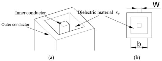
Figure 1.
(a) A 3D isometric view of the square-coaxial line filled with dielectric material between inner and outer conductors; (b) dimensions of the square-coaxial line and is the relative dielectric constant of the filled material.
Figure 2a shows the TEM-line model used to feed our MBAs. In the model, the bottom end of the feed-line is closed by a metal plate. A few FD-TD grids above the inner surface of the metal plate, i.e., at plane 3, the Mur’s first order absorbing boundary condition (ABC) is applied. Since we know the TEM wave speed, the wave that comes down along the TEM-line can be adequately absorbed by the ABC. In addition, as the bottom end is closed by the metal plate, any unreal wave in between plane 3 and the plate’s inner surface inside the TEM-line cannot enter the computational domain outside the TEM-line. Therefore, it cannot “pollute” the FD-TD calculations, such as the radiation pattern calculation. Hence, the end metal plate and the ABC form a numerical matched-load for our FD-TD calculations. To test the performance of the-load, a voltage source is placed at plane 1, and the incident and reflected waves are sampled at plane 2. During the test, the length of the TEM-line makes the top open-end far away from plane 2. This ensures that the entire reflected wave from the numerical matched-load passes plane 2 before the reflected wave from the open-end arrives. Figure 2b shows a Gaussian pulse that passes through plane 2 after about 1000 time-steps, and after 2400 time-steps, the reflected wave from the numerical matched-load is sampled at plane 2 (Figure 2c). After about 2670 time-steps, the entire reflected wave from the numerical matched-load passes plane 2, and until then, the reflection from the open end of the coax has not reached plane 2. The return loss of the-load is shown in Figure 2d, which shows a good performance, i.e., return loss <−50 dB in the frequency range of interest of this study, and can be used to terminate the feed line. In this test, the 0.1 mm cube uniform grid was used with a time-step of 1.6678 × 10⁻¹³ s. These numbers were also used for all FD-TD calculations in the study. The reason for picking such a grid size is that it gives about 28.89 grids per wavelength at 70 GHz in the dielectric marital with = 2.2. Note that, when the TEM-line model was used to feed MBAs during the FD-TD simulations, plane 1 and plane 2 were changed to the sampling plane and source plane, respectively.
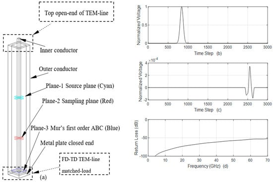
Figure 2.
(a) A 3D isometric view of the TEM feed-line; (b) An example of normalized incident Gaussian pulse launched from Plane-1 and collected at Plane-2; (c) The reflected wave from the FD-TD numerical matched-load (normalized to the maximum value in (b)) and collected at Plane-2; (d) The return loss of the FD-TD numerical matched-load (see the text for more details).
Figure 3 shows the details of the biconical structure fed by the TEM-line model. The inner and outer conductors of the TEM-line are connected to the apex areas of the upper and the lower cones, respectively. The cone-angle and other dimensions are also given in the figure. Both upper and lower cones have the same cone-angle. It also shows that the metal cones are constructed by small metallic (in yellow color) blocks that can be formed by at least one 0.2 mm cube so that (1) the FD-TD calculations can have a uniform mesh with dx = dy = dz = 0.1 mm, and (2) the structure can be fabricated with 3D laser metal additive fabrication technology that has 0.2 mm or less fabrication step. Note that:
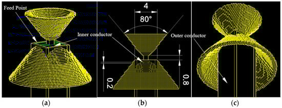
Figure 3.
(a) An isometric view close to the antenna feeding point (from an upper looking angle), yellow and green colors indicate metal and dielectric material; (b) the front-view and dimensions in mm; (c) another isometric view from a lower looking angle.
- This figure just shows very small parts of the cones, and both cones are extended further, as shown in Figure 4;
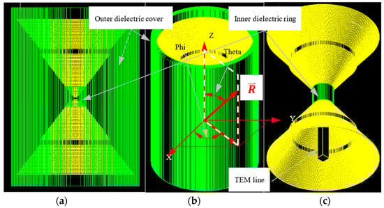 Figure 4. (a) A front wireframe view of the base-modified biconical antennas (MBA) with stair-cased inner dielectric ring (in green color) and outer dielectric cover (also in green color); (b) an isometric view of the base MBA (looking from an upper angle) with XYZ-coordinate system, a [phi theta] angle-pair shows the direction of the vector and the white-dashed parallelogram shows a portion of the phi-cutting plane, on which 2D radiation pattern is calculated in Section 3 and Section 4; (c) an isometric view of the base MBA without outer dielectric cover (looking from a lower angle). All dielectric materials have = 2.2.
 - In order to show how the inner conductor is connected to the upper cone, the dielectric material inside the TEM-line shows the same height as the edge of the outer connector in Figure 3a,b;
- In all our MBA designs, the dielectric material is extended outside the TEM-line outer conductor by 0.8 mm, which can be seen in Figure 5a and Figure 13a;
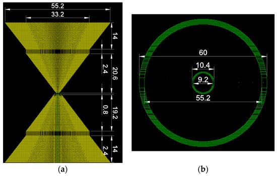 Figure 5. (a) The dimensions of modified cones in the base MBA, the total height of two cones is 73.4 mm, and the dielectric insert (green) sticks out at the end of the feed-line by 0.8 mm; (b) the top view of the discretized inner dielectric ring and the outer dielectric cover (unit is in mm).
 - Finally, although from a distant view, the antenna looks like having a symmetric structure, as shown in Figure 4, all MBA structures in our designs have three minor asymmetries:
- Because of the feed-line, the upper and lower cones are not exactly mirror-imaged with respect to feed-point;
- Since the square-shape of the outer conductor of the TEM-line, the structure does not have rotational symmetry with respect to the phi-angle (defined in Figure 4b) in each quadrant, and;
- Since the 0.2 mm cube is used to discretize curved cone surfaces, it results in the stair-cased outer surfaces of the cones, which do not have rotational symmetry with respect to the phi-angle in each quadrant, as well. This can be clearly observed in Figure 3a.
3. Base MBA Structure, Its Antenna Characteristics and Comparison of the Results Obtained from Two FD-TD Solvers
3.1. Structure and Dimensions
Figure 4 shows the base MBA, which has a modified metal biconical structure, a TEM-line inside the bottom cone, a dielectric inner ring (in green color) and a dielectric outer cover (in green color). The dimensions of the structure are given in Figure 5. The height of the inner dielectric ring is 9.4 mm, which both ends just touch the metal cones, as one can see from Figure 4a,c.
The total length of the cover is 84.2 mm, which is 10.8 mm longer than the modified biconical structure, i.e., each side is 5.4 mm over the edge of the cone. The circular-shapes to get the discretized versions of the inner ring and the outer cover shown in Figure 5b are the 4.6 mm radius circle with a wall of 0.6 mm thickness and the 27.6 mm radius circle with a wall of 2.4 mm thickness, respectively. It should be mentioned that the discretized versions of the inner dielectric ring and the outer cover also show asymmetries with respect to the phi-angle. Figure 6 shows the base MBA modeled inside GEMS.
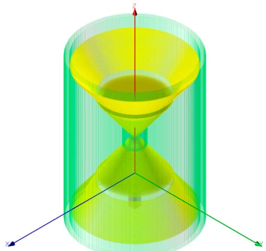
Figure 6.
The base MBA is modeled in General-Purpose EM solver (GEMS); the green parts are dielectric material, and the yellow parts are modified metal cones and TEM-line.
3.2. VSWR and Return Loss of the Base MBA
The VSWR and return loss of the base MBA obtained from both FD-TD solvers are shown in Figure 7. An excellent agreement between the two results can be observed. From the figure, one can also see that from 6.14 GHz to 68.27 GHz, the antenna has VSWR ≤ 2. In addition, in the lower frequency, there are two frequency bands that have VSWR ≤ 2, as shown in Figure 8. They are [0.93, 1.23] GHz and [3.97, 5.36] GHz. Note that the length of the base MBA changes from 0.97 GHz to 1.31 GHz wavelength from 3.97 GHz to 5.36 GHz. This means that the wavelength of any band lower than [3.97, 5.36] GHz band is bigger than the length of the base MBA.
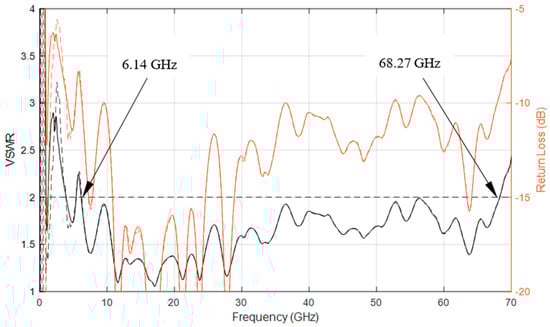
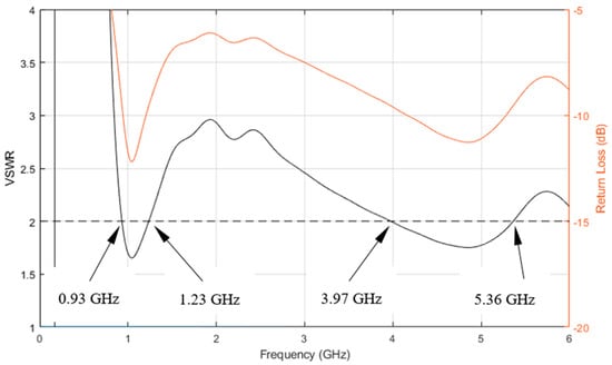
Figure 8.
Details of voltage standing wave ratio (VSWR) and return loss from 0 GHz to 6 GHz of the base MBA showed solid lines in Figure 7.
The input characteristics of the modified radiation structures from the base MBA, i.e., (1) without the inner dielectric ring and the outer dielectric cover and (2) just having the inner dielectric ring without the outer dielectric cover, are shown in Figure 9a,b, respectively. Comparing these with the results in Figure 7 shows the following:
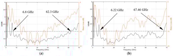
Figure 9.
The input characteristics of the radiation structures (a) the base MBA without dielectric ring and cover, and (b) the base MBA just with the inner dielectric ring.
- Without any dielectric ring and cover, the TEM-line-fed modified biconical structure also has a wideband with VSWR ≤ 2 from 6.8 GHz to 62.3 GHz. However, practically this structure cannot hold by itself as an EM radiation device.
- Once the inner dielectric ring is added, the band with VSWR ≤ 2 is extended to [6.22, 67.46] GHz, which is very close to the base MBA result of [6.14, 68.27] GHz.
- The beginning and ending frequency points of the two bands with VSWR ≤ 2 that are lower than 6 GHz in the three radiation structures, i.e., without any dielectric materials, just having an inner dielectric ring and the base MBA, are [0.95, 1.29] GHz and [3.59, 5.24] GHz, [0.95, 1.29] GHz and [3.55, 5.36] GHz, and [0.93, 1.23] GHz and [3.97, 5.36] GHz, respectively. These indicate that the dielectric cover plays some role, but not very significant, in the locations of two lower VSWR bands.
3.3. Far-Field Radiation Patterns
The normalized far-field radiation patterns of the base MBA are shown in this section. Patterns at the beginning, middle and end of the two lower bands with VSWR ≤ 2, i.e., [0.93; 1.08; 1.23] GHz and [3.97; 4.67; 5.36] GHz, are presented in Figure 10. Since there are too many patterns between 6.14 GHz and 68.27 GHz to be shown here, more patterns are shown in Appendix A at 7 GHz, 10 GHz, 17 GHz, 22 GHz, 27 GHz, 37 GHz, 47 GHz, 52 GHz, 57 GHz and 67.0 GHz frequency points. Note that:
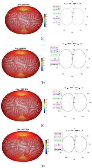
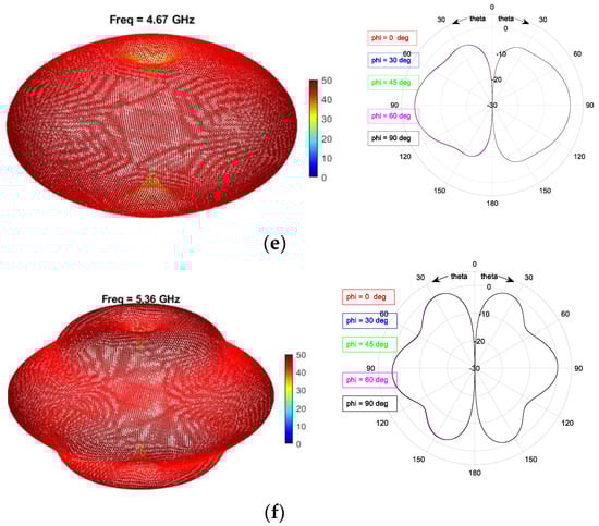
Figure 10.
3D patterns of the base MBA obtained by our FD-TD solver (left column) and 2D patterns (right column) at different phi-cutting planes (shown by different colors) at the beginning, middle and end frequency points of two lower bands with VSWR ≤ 2. In all 2D plots, our FD-TD and GEMS results are plotted on the right and left sides, respectively. Subplots (a–f) are far field patterns at 0.93 GHz, 1.08 GHz, 1.23 GHz, 3.97 GHz, 4.67 GHz and 5.36 GHz, respectively.
- All the radiation patterns are normalized to the maximum value obtained from vertical (EV) fields in the current plot;
- All 3D patterns are scaled into [0, 30] dB since the 3D scatter-plot cannot show a negative value. After scaling, any field values less than 0 dB in 3D patterns are set to 0 dB;
- All 2D patterns are scaled into [−30, 0] dB. After normalization, any field values less than −30 dB are set to −30 dB;
- All the 3D patterns are plotted using a 3D scatter-plot. There are a total of 40,962 directions defined by [phi theta] pairs (see Figure 4b), and these angle pairs are obtained from the vertices of an icosphere. This gives close to uniformly distributed directions compared to the UV-sphere [37] defined directions that have much denser directions closer to the north- and south-poles than at the equator. More details of icosphere defined directions can be found in [38,39].
From the plots shown in Figure 10 and Appendix A, one can have the following observations:
- The 2D radiation patterns at different frequencies obtained by the two FD-TD solvers have an excellent agreement;
- Omnidirectional donut-shaped radiation patterns appear in the band of [0.93, 1.23] GHz, as the wavelength is bigger than the length of the base MBA;
- In the second band, [3.97, 5.36] GHz, the omnidirectional donut-shaped can be observed at the beginning of the band and starts giving ripples, especially in the upper half of the band. It is because the modified biconical structure is about one wavelength at the beginning of the band and reaches about 1.31 wavelength at the end of the band:
- The horizontal polarization (H-pol) in these bands are all 30 dB less than or equal to the maximum value of the V-pol. Hence, there are no H-pol patterns shown on the 2D plots in Figure 10;
- As shown in Appendix A, when the frequency increases in the ultra-wideband, [6.14, 68.27] GHz,
- The base MBA cannot provide a pure donut-shaped omnidirectional radiation pattern anymore, i.e., the V-pol radiation patterns at different phi-cutting planes are different from each other. This phenomenon becomes clearer when the frequency becomes higher, see Figure A1i,j. This is because the TEM-line feed structure and the discretized version of modified cones are not symmetric with respect to phi-angles in each quadrant, and when wavelength gets smaller, these asymmetric structural properties have more inference on the antenna radiation property.
- The H-pol is also increased. Again, it can be observed in Figure A1i,j.
- The higher H-pol may appear at around phi = 30° and 60° in the first quadrant, as the magenta and blue colored patterns are dominant in the 2D plots from Figure A1i,j. Since the radiation structure has 90° rotational symmetry in phi-angle, we can expect that strong H-pol can also occur around phi = (120° and 150°), (210° and 240°) and (300° and 330°) angular ranges in the second, third and fourth quadrants, respectively.
- At the higher frequency end, there are no clear donut-shaped patterns, and many ripples appear in both phi and theta directions. This is caused by the combined effects from (1) the size of the structure becomes much bigger than the wavelength, (2) the asymmetric structural properties discussed in Section 2, and (3) the surface current that appears on the cones create some ring-like standing-wave patterns, which can be seen from the surface current distributions on the upper cones of the base MBA at different frequency points in the ultra-wideband as shown in Figure 15.
- Again, due to the combined effects discussed in the previous item, some deep-notches can appear in theta between 60° and 120°. Figure A1h shows an example.
The calculated maximum antenna gains for V-pol and H-pol are shown in Figure 11. From the figure, one can find that the base MBA has dominant V-pol, and its maximum gain is between 2 dBi to 6 dBi in [3.97, 5.36] GHz and [6.14, 28.27] GHz bands.
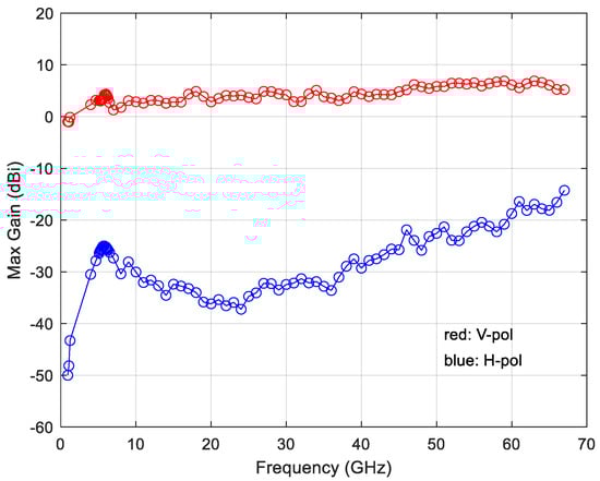
Figure 11.
The calculated base MBA maximum gains.
4. Metallic-Ring-Loaded MBAs and Their Antenna Characteristics
4.1. Structures and Dimensions
To create more bands and change the frequency band locations in the lower frequency end, metallic-rings can be added at both circular-ends of the cones. Figure 12 shows the metallic-ring structure, which has the same size as that of the circular-ends of the two cones. The height of the ring is 5 mm. It has four 2.4 mm × 5.4 mm pads that touch the ends of two cones, as shown in Figure 13a.
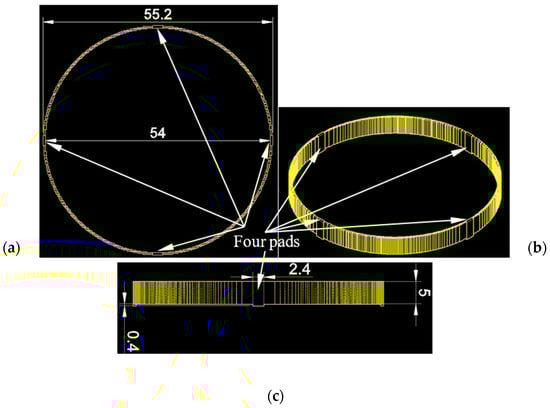
Figure 12.
The discretized metallic-ring and its dimensions, (a) the top view, (b) an isometric view and (c) a side view (unit is in mm).
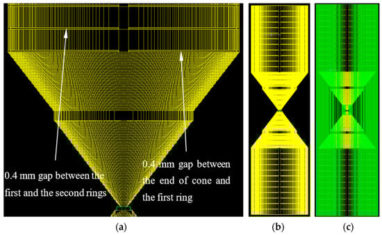
Figure 13.
(a) Details of how the metallic rings are stacked to the base MBA; (b) a view of the base MBA with 12 rings (to be called 24-ring-loaded MBA) on each side of the cone without inner dielectric ring and cover; (c) a wireframe view of the 24-ring-loaded MBA with both inner dielectric ring and cover. The total length of the 24-ring-loaded MBA is 203 mm, which is about 0.3 wavelength of the low end of frequency.
Note that, Figure 13 also shows that the dielectric material (green color) inside the TEM-line is extended outside the outer conductor of the TEM-line. The length of the extended portion is 0.8 mm, which is the same as in Figure 5a.
Figure 13c shows that the length of the outer dielectric cover is the same as the length of the 24-ring-loaded MBA. This also applies to the other number of ring-loaded MBAs. Although equal numbers of metallic-rings are added on both sides of cones in the study, an unequal number of metallic-rings also can be added. Their results will not be reported in this paper.
4.2. VSWR and Return Loss of Metallic-Ring-Loaded MBAs
Figure 14 compares the return losses and VSWRs of MBAs with a different number of rings in [4, 70] GHz. It appears that the different ring-loaded MBAs have almost the same input characteristics as those of the base MBA.
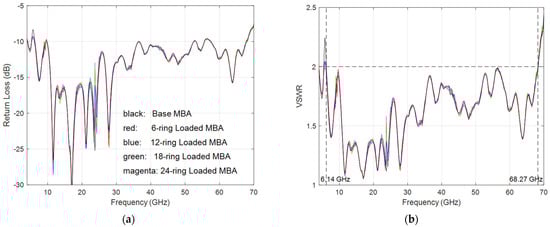
Figure 14.
(a) Return loss and (b) VSWR of metallic-ring-loaded MBAs with an equal number of rings on both sides of the base MBA.
- In the [3.97, 5.36] GHz band, the details of starting, middle and ending frequencies are given in the last column of Table 1. In this band, these radiation structures work more in the transition between resonant mode and “traveling-wave” modes;
 Table 1. The starting, middle and ending frequencies of bands in frequency less than 6 GHz.
 - In the [6.14, 68.27] GHz band, these radiation structures work mostly in the “traveling-wave” mode, i.e., before the wave reaches the ends of cones, the majority of the electromagnetic energy has been radiated by the modified-biconical part of the antenna. This also can be observed from the surface current distributions on the upper cones of MBAs shown in Figure 15.
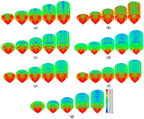 Figure 15. The normalized surface current distributions on the upper cones of the base, 6-ring, 12-ring, 18-ring, and 24-ring-loaded MBAs (from left to right) at (a) 7 GHz, (b) 17 GHz, (c) 27 GHz, (d) 37 GHz, (e) 47 GHz, (f) 57 GHz and (g) 67 GHz in the ultra-wideband. Note that, in order to show clearer current distributions, the figure only shows the current distribution values less than or equal to 0.4077, as the higher values more concentrate near the tips of upper cones.
Figure 15 shows the upper cone surface current distributions at seven frequencies in the [6.14, 68.27] GHz band. Comparing the results of the base MBA (left) and other ring-loaded MBAs at each frequency shows that the surface current distributions are very close to each other in the [6.14, 68.27] GHz band. For ring-loaded MBAs, the currents on rings are much weaker than those on the modified cones. This explains:
- Why the input characteristics of the base and ring-loaded MBAs are almost the same, and;
- Why the radiation patterns obtained from the base and ring-loaded MBAs are similar (this will be shown in the next section) in the [6.14, 68.27] GHz band.The figure also shows that as frequency increases in the [6.14, 68.27] GHz band,
- The main current that contributes to the far-field patterns gets closer to the feed point, and;
- More current-rings or the standing-wave patterns appear on the cones, which cause ripples and even notches in the theta-direction of the radiation patterns.
The same comparison, as shown in Figure 14, for lower frequency bands are shown in Figure 16. It can be found that these radiation structures create a number of bands with VSWR ≤ 2 when the frequency is lower than 4 GHz, and these bands with VSWR ≤ 2 move towards the lower frequency when more metallic-rings are added. It is obvious that the characteristics of resonant modes have appeared here; as the length of the structure increases, the operational frequency bands move towards the lower frequency. Table 1 gives the starting, middle and ending frequency points of those bands with VSWR ≤ 2 for different numbers of metallic-ring-loaded MBAs. The surface current distributions of the middle frequency point (see Table 1) in each band with VSWR ≤ 2 are shown in Figure 17.
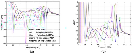
Figure 16.
(a) Return loss and (b) VSWR of metallic-ring-loaded MBAs with an equal number of rings on both sides of the base MBA when the frequency is lower than 4 GHz.
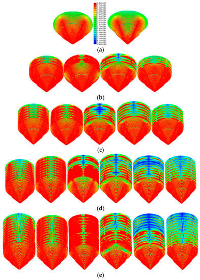
Figure 17.
The surface current distributions on the upper cones of the (a) base, (b) 6-ring, (c) 12-ring, (d) 18-ring, and (e) 24-ring-loaded MBAs at the middle frequency from band 1 to band 6 in Table 1.
4.3. Far-Field Radiation Patterns
The far-field radiation patterns of the middle-frequency point in each of the lower bands for 6-ring, 12-ring and 24-ring-loaded MBAs are shown in Figure 18, Figure 19 and Figure 20, respectively. Similar to the base MBA case, 2D radiation patterns of 6-ring, 12-ring, 18-ring and 24-ring-loaded MBAs at 7 GHz, 10 GHz, 17 GHz, 22 GHz, 27 GHz, 37 GHz, 47 GHz, 52 GHz, 57 GHz and 67 GHz frequency points are shown in Appendix B.
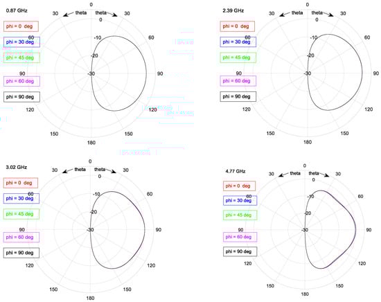
Figure 18.
The patterns of the 6-ring-loaded MBA at middle-frequency points of four bands with VSWR ≤ 2 in Table 1.
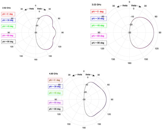
Figure 19.
The radiation patterns of the 12-ring-loaded MBA at middle-frequency points of five bands with VSWR ≤ 2 in Table 1.
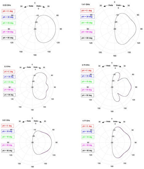
Figure 20.
The radiation patterns of 24-ring-loaded MBA at middle-frequency points of six bands with VSWR ≤ 2 in Table 1.
- When the length of MBA is less than one wavelength, the omnidirectional donut-shaped radiation patterns can be produced with more pure vertical polarization;
- When the length is around one wavelength, the donut shape becomes flatter;
- When the length is bigger than one wavelength, the donut shape is modified with ripples;
- In these plots, the H-pol component is still at least 30 dB lower than the maximum value of V-pol, as the H-pol is not shown in these plots.
Comparing the 2D patterns in Appendix B and the patterns in the right column in Appendix A, we can see that the ring-loaded MBAs have close or similar to base MBA V-pol patterns, especially when theta is in between 30° to 120° as frequency increases. This tells that in the [6.14, 68.27] GHz band, the modified cone surfaces contain the most electric surface current (see Figure 15) that contributes to the V-pol far-field patterns. Compared to the base MBA, the H-pol of the ring-loaded MBAs increases due to the introduction of extra 0.4 mm gaps by the rings, as shown in Figure 13. These gaps create some currents along phi-direction on the surface of rings, which increase H-pol for ring-loaded MBAs.
Table 2 summarizes the FD-TD calculation information and the cost for the base and ring-loaded MBAs. Two kinds of computers were used for the calculations. Although the FD-TD method may take a long time to obtain the results, it produces the time-domain input characteristics, which can be used to calculate the input characteristics of MBAs at any frequency up to 70 GHz. In addition, the far-field patterns at any frequency point can be obtained using the surface equivalence theory, time-domain near-to-far-field transformation and Fourier Transform during an FD-TD simulation. For example, the frequency points can include those frequencies given in Table 1 and frequencies from 7 GHz to 67 GHz with 1 GHz interval. It is the same for surface current distribution calculations. The time-domain far-field data and surface current data can also be collected during the simulation. If many radiation directions are required for the far-field patterns, and many surface areas need to be viewed for the surface current on the antenna, then the time-domain data collections will require much more computer resources. However, once these time-domain data are collected, one can obtain the far-field patterns and surface current distributions of the antenna at any frequency of interest.
Table 2.
Information of computational time, costs and used resources.
5. Conclusions
Using the FD-TD method, new MBA structures fed by a close to 50 ohm TEM-line are studied numerically in this paper. Two independently developed FD-TD solvers are used in the study, and they produce almost identical simulation results for the base MBA structure. In our design, by adding a different number of metallic-rings on the base MBA, the radiation structures can have up to five tunable bands with VSWR ≤ 2 between 0.4 GHz and 4 GHz, about 1.39 GHz band with VSWR ≤ 2 from 3.97 GHz to 5.36 GHz, as well as, an extremely wideband from 6.14 GHz to 68.27 GHz. At those lower frequency bands, the antennas work in their resonant mode and produce donut-shaped or close to donut-shaped V-pol radiation patterns with better than 30 dB cross-polarization. In the [6.14, 68.27] GHz band, the MBAs work mainly in their “traveling-wave” mode. When the frequency increases in the band, many ripples appear on radiation patterns, and the cross-polarization gets worse. The unique feature of our design is that the input characteristics and far-field V-pol patterns do not have significant changes by adding a different number of metallic-rings in the band of [6.14, 68.27] GHz. The simulation result shows that the maximum V-pol gain is about or lower than 0 dBi in those low-frequency bands and is between 2 dBi and 6 dBi in the [6.14, 68.27] GHz band. The 3D metal additive manufacturing/3D printing method also has been considered to build these antennas in the near future.
Author Contributions
C.W. and J.E. have made contributions to the conceptualization, methodology, formal analysis, investigation and reviewing and editing of the article, and C.W. wrote the original draft of the article. Both authors have read and agreed to the published version of the manuscript.
Funding
This research was supported by the Radar Electronic Warfare Capability Development in Radar Electronic Warfare Section, Defense Research and Development Canada—Ottawa Research Center, Department of National Defense Canada.
Data Availability Statement
All the detailed antenna structures and materials are available in the paper.
Acknowledgments
Authors would-like to gracefully thank Wen-Hua Yu for allowing us to use the general-purpose EM solver for this study.
Conflicts of Interest
The authors declare no conflict of interest.
Appendix A. Far-Field Radiation Patterns of the Base MBA in Its Ultra-Wideband
In the following plots, the left column shows 3D V-pol patterns, and the right column shows 2D patterns at phi = 0°, 30°, 45°, 60° and 90° cutting planes in the first quadrant. In 2D plots, the right-side patterns were obtained by our FD-TD solver, and those on the left side were calculated by the GEMS. Both H-pol and V-pol patterns on those 2D cutting planes are shown in each 2D plot. One can see that the H-pol gets bigger when the frequency is increased. The H-pol appears higher than −30 dB in Figure A1i,j compared to the maximum value of V-pol in each 2D plot.


Figure A1.
Subplots (a–j) are the far field radiation patterns of the base MBA at 7 GHz, 10 GHz, 17 GHz, 22 GHz, 27 GHz, 37 GHz, 47 GHz, 52 GHz, 57 GHz and 67 GHz, respectively.
Figure A1.
Subplots (a–j) are the far field radiation patterns of the base MBA at 7 GHz, 10 GHz, 17 GHz, 22 GHz, 27 GHz, 37 GHz, 47 GHz, 52 GHz, 57 GHz and 67 GHz, respectively.


Appendix B. 2D Radiation Patterns of 6-Ring-, 12-Ring-, 18-Ring- and 24-Metallic-Ring-Loaded MBAs from 6.14 GHz to 68.27 GHz
In the following figures, there are two plots in each figure for the frequency given in the figure caption. The left and right 2D patterns in the left-plot of each figure are V- and H-pol patterns of 6- and 12-ring-loaded MBA, respectively. The same 2D patterns for 18-and 24-ring-loaded MBAs are shown in the right-plot of each figure. All the patterns are sampled in the first quadrat at the phi = 0°, 30°, 45°, 60°, and 90° cutting planes.

Figure A2.
2D patterns at 7 GHz of 6-, 12-, 18- and 24-ring-loaded MBA in different cutting planes.
Figure A2.
2D patterns at 7 GHz of 6-, 12-, 18- and 24-ring-loaded MBA in different cutting planes.


Figure A3.
2D patterns at 10 GHz of 6-, 12-, 18- and 24-ring-loaded MBA in different cutting planes.
Figure A3.
2D patterns at 10 GHz of 6-, 12-, 18- and 24-ring-loaded MBA in different cutting planes.


Figure A4.
2D patterns at 17 GHz of 6-, 12-, 18- and 24-ring-loaded MBA in different cutting planes.
Figure A4.
2D patterns at 17 GHz of 6-, 12-, 18- and 24-ring-loaded MBA in different cutting planes.


Figure A5.
2D patterns at 22 GHz of 6-, 12-, 18- and 24-ring-loaded MBA in different cutting planes.
Figure A5.
2D patterns at 22 GHz of 6-, 12-, 18- and 24-ring-loaded MBA in different cutting planes.


Figure A6.
2D patterns at 27 GHz of 6-, 12-, 18- and 24-ring-loaded MBA in different cutting planes.
Figure A6.
2D patterns at 27 GHz of 6-, 12-, 18- and 24-ring-loaded MBA in different cutting planes.


Figure A7.
2D patterns at 37 GHz of 6-, 12-, 18- and 24-ring-loaded MBA in different cutting planes.
Figure A7.
2D patterns at 37 GHz of 6-, 12-, 18- and 24-ring-loaded MBA in different cutting planes.


Figure A8.
2D patterns at 47 GHz of 6-, 12-, 18- and 24-ring-loaded MBA in different cutting planes.
Figure A8.
2D patterns at 47 GHz of 6-, 12-, 18- and 24-ring-loaded MBA in different cutting planes.


Figure A9.
2D patterns at 52 GHz of 6-, 12-, 18- and 24-ring-loaded MBA in different cutting planes.
Figure A9.
2D patterns at 52 GHz of 6-, 12-, 18- and 24-ring-loaded MBA in different cutting planes.


Figure A10.
2D patterns at 57 GHz of 6-, 12-, 18- and 24-ring-loaded MBA in different cutting planes.
Figure A10.
2D patterns at 57 GHz of 6-, 12-, 18- and 24-ring-loaded MBA in different cutting planes.


Figure A11.
2D patterns at 67 GHz of 6-, 12-, 18- and 24-ring-loaded MBA in different cutting planes.
Figure A11.
2D patterns at 67 GHz of 6-, 12-, 18- and 24-ring-loaded MBA in different cutting planes.

References
- Saeidi, T.; Ismail, I.; Wen, W.P.; Alhawari, A.R.H.; Mohammadi, A. Ultra-wideband antenna for wireless communication applications. Hindawi Int. J. Antenna Propag. 2019, 25. [Google Scholar] [CrossRef]
- Linag, X.L. Ultra-Wideband Antenna and Design; IntechOpen: London, UK, 3 October 2012. [Google Scholar] [CrossRef]
- Lodge, O. Electric Telegraphy. U.S. Patent 609,154, 16 August 1898. [Google Scholar]
- Kudpok, R.; Sachon, S.; Siripon, N.; Kosulvit, S. Design of a compact biconical antenna for UWB applications. In Proceedings of the International Symposium on Intelligent Signal Processing and Communication Systems (ISPACS), Chiang Mai, Thailand, 7–9 December 2011; 6p. [Google Scholar] [CrossRef]
- Liu, N.; Zhang, Z.; Fu, G.; Liu, Q.; Wang, L. A compact biconical antenna for ultra-wideband applications. In Proceedings of the 2013 5th IEEE International Symposium on Microwave, Antenna, Propagation and EMC Technologies for Wireless Communications, Chengdu, China, 29–31 October 2013; pp. 327–332. [Google Scholar] [CrossRef]
- Zhekov, S.S.; Tatomirescu, A.; Pedersen, G.F. Modified biconical antenna for ultra-wideband applications. In Proceedings of the 10th European Conference on Antennas and Propagation (EuCAP), Davos, Switzerland, 10–15 April 2016; 5p. [Google Scholar] [CrossRef]
- Santos, H.; Pinho, P.; Salgado, H. Patch Antenna-in-Package for 5G Communications with dual polarization and high isolation. Electronics 2020, 9, 1223. [Google Scholar] [CrossRef]
- Khan, A.; Geng, S.; Zhao, X.; Shah, Z.; Jan, M.U.; Abdelbaky, M.A. Design of MIMO antenna with an enhanced isolation technique. Electronics 2020, 9, 1217. [Google Scholar] [CrossRef]
- Jeffrey, C.S.; Kufre, M.U.; Akaninyene, B.O. Compact rectangular slot patch antenna for dual frequency operation using inset feed technique. Int. J. Inf. Commun. Sci. 2016, 1, 47–53. [Google Scholar]
- Camacho-Gomez, C.; Sanchez-Montero, R.; Martínez-Villanueva, D.; López-Espí, P.L.; Salcedo-Sanz, S. Design of a multi-band microstrip textile patch antenna for LTE and 5G services with the CRO-SL ensemble. Appl. Sci. 2020, 10, 1168. [Google Scholar] [CrossRef]
- Reineix, A.; Jecko, B. Analysis of microstrip patch antennas using finite difference time domain method. IEEE Trans. Antennas Propag. 1989, 11, 1361–1369. [Google Scholar] [CrossRef]
- Maloney, J.G.; Smith, G.S.; Scott, W.R., Jr. Accurate computation of the radiation from simple antennas using the finite-difference time-domain method. IEEE Trans. Antennas Propag. 1990, 7, 1059–1068. [Google Scholar] [CrossRef]
- Katz, D.S.; Piket-May, M.J.; Taflove, A.; Umashankar, K.R. FDTD analysis of electromagnetic wave radiation from systems containing horn antennas. IEEE Trans. Antennas Propag. 1991, 8, 1203–1212. [Google Scholar] [CrossRef]
- Tirkas, P.A.; Balanis, C.A. Finite-difference time-domain method for antenna radiation. IEEE Trans. Antennas Propag. 1992, 3, 334–340. [Google Scholar] [CrossRef]
- Wu, C.; Wu, K.L.; Bi, Z.Q.; Litva, J. Accurate characterization of planar printed antennas using finite-difference time-domain method. IEEE Trans. Antennas Propag. 1992, 40, 526–534. [Google Scholar] [CrossRef]
- Kim, J.; Yoon, T.; Kim, J.; Choi, J. Design of an ultra-wideband printed monopole antenna using FDTD and genetic algorithm. IEEE Microw. Wirel. Compon. Lett. 2005, 15, 395–397. [Google Scholar]
- Taflove, A.; Hagness, S.C. Computational Electrodynamics: The Finite-Difference Time-Domain Method, 2nd ed.; Artech House: Norwood, MA, USA, 2000. [Google Scholar]
- Jamali, J.; Tayarzade, N.; Moini, R. Analyzing of Conical Antenna as an Ultra-Wideband Antenna Using Finite Difference Time Domain Method. In Proceedings of the 2007 International Conference on Electromagnetics in Advanced Applications ICEAA’07, Torino, Italy, 17–21 September 2007; pp. 994–997. [Google Scholar]
- Yang, C.; Guo, Q.; Huang, K. Miniature omnidirectional ultra-wideband antenna. In Proceedings of the 2010 International Conference on Microwave and Millimeter Wave Technology, Chengdu, China, 8–11 May 2010; pp. 969–971. [Google Scholar]
- Frazier, W.E. Metal additive manufacturing: A review. J. Mater. Eng. Perform. 2014, 23, 1917–1928. [Google Scholar] [CrossRef]
- Wu, S.-Y.; Yang, C.; Hsu, W.; Lin, L. 3D-printed microelectronics for integrated circuitry and passive wireless sensors. Microsyst. Nanoeng. 2015, 1. [Google Scholar] [CrossRef]
- Wu, C.; Litva, J.; Wu, K.-L. An application of FD-TD method for studying the effects of packages on the performance of microwave and high speed digital circuits. IEEE Trans. Microw. Theory Tech. 1994, 42, 2007–2009. [Google Scholar] [CrossRef]
- Wu, C. Printed Antenna Structure for Wireless Data Communications. U.S. Patent 6,008,774, 28 December 1999. [Google Scholar]
- Wu, C.; Litva, J. Feed Structure for Tapered Slot Antennas. U.S. Patent 6,317,094, 13 November 2001. [Google Scholar]
- Wu, C. Low Profile Waveguide Network for Antenna Array. U.S. Patent 6,563,398, 13 May 2003. [Google Scholar]
- Yee, K. Numerical solution of initial boundary value problems involving maxwell’s equations in isotropic media. IEEE Trans. Antennas Propag. 1966, 14, 302–307. [Google Scholar]
- Berenger, J.-P. A perfectly matched layer for the absorption of electromagnetic waves. J. Comput. Phys. 1994, 114, 185–200. [Google Scholar] [CrossRef]
- Yu, W.; Mittra, R.; Su, T.; Liu, Y.; Yang, X. Parallel Finite-Difference Time-Domain Method; Artech: Norwood, MA, USA, 2006. [Google Scholar]
- Mittra, R.; Yu, W.H.; Lu, Y.Q.; Lu, R. GEMS—A general purpose conformal FDTD solver tailored for parallel platforms. In Proceedings of the IEEE 2008 Asia-Pacific Symposium on Electromagnetic Compatibility and 19th International Zurich Symposium on Electromagnetic Compatibility, Singapore, 19–23 May 2008. [Google Scholar]
- Yu, W.H.; Yang, X.L.; Li, W.X. Advanced feature to enhance the FDTD method in GEMS simulation software package. In Proceedings of the 2012 IEEE International Symposium on Antennas and Propagation, Chicago, IL, USA, 8–14 July 2012. [Google Scholar] [CrossRef]
- Green, H. The Characteristic Impedance of Square Coaxial Line (Correspondence). IEEE Trans. Microw. Theory Tech. 1963, 11, 554–555. [Google Scholar] [CrossRef]
- Schneider, M. Computation of Impedance and Attenuation of TEM-Lines by Finite Difference Methods. IEEE Trans. Microw. Theory Tech. 1965, 13, 793–800. [Google Scholar] [CrossRef]
- Lau, K. Technical memorandum. Loss calculations for rectangular coaxial lines. IEE Proc. H Microw. Antennas Propag. 1988, 135, 207. [Google Scholar] [CrossRef]
- Llamas-Garro, I.; Lancaster, M.; Hall, P. Air-filled square coaxial transmission line and its use in microwave filters. IEE Proc. Microw. Antennas Propag. 2005, 152, 155. [Google Scholar] [CrossRef]
- Navarro, E.A.; Such, V.; Gimeno, B.; Cruz, J.L. T-junction in square coaxial waveguide: A FD-TD approach. IEEE Trans. Microw. Theory Tech. 1994, 42, 347–350. [Google Scholar] [CrossRef]
- Navarro, E.A.; Wu, C.; Chung, P.; Litva, J. Sensitivity analysis of the non-orthogonal FDTD method applied to the study of square coaxial waveguide structures. Microw. Opt. Technol. Lett. 1995, 8, 138–140. [Google Scholar] [CrossRef]
- Blender, What Is the Difference between a UV Sphere and Icosphere? Available online: https://blender.stackexchange.com/questions/72/what-is-the-difference-between-a-uv-sphere-and-an-icosphere (accessed on 20 June 2020).
- Wu, C.; Elangage, J. Multi-emitter two-dimensional angle-of-arrival estimator via compressive sensing. IEEE Trans. Aerosp. Electron. Syst. 2020, 56, 2884–2895. [Google Scholar] [CrossRef]
- Wu, C.; Elangage, J. Nonuniformly spaced array with the direct data domain method for 2D angle-of-arrival measurement in electronic support measures application from 6 to 18 GHz. Hindawi Int. J. Antennas Propag. 2020, 2020, 1–23. [Google Scholar] [CrossRef]


Publisher’s Note: MDPI stays neutral with regard to jurisdictional claims in published maps and institutional affiliations. |
© 2021 by the authors. Licensee MDPI, Basel, Switzerland. This article is an open access article distributed under the terms and conditions of the Creative Commons Attribution (CC BY) license (http://creativecommons.org/licenses/by/4.0/).