
Wideband Rectangular Waveguide to Substrate Integrated Waveguide (SIW) E-Plane T-Junction


Abstract
1. Introduction
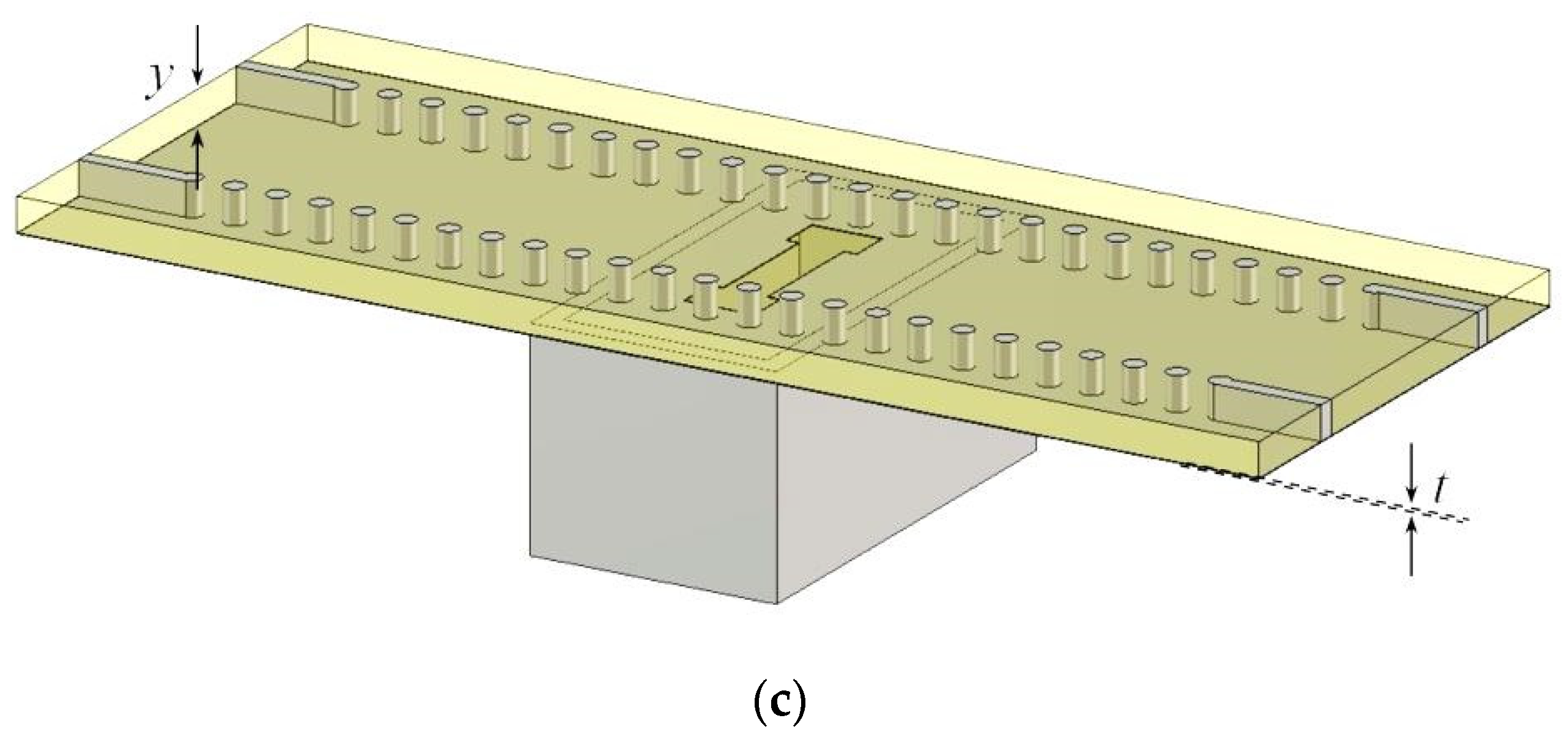
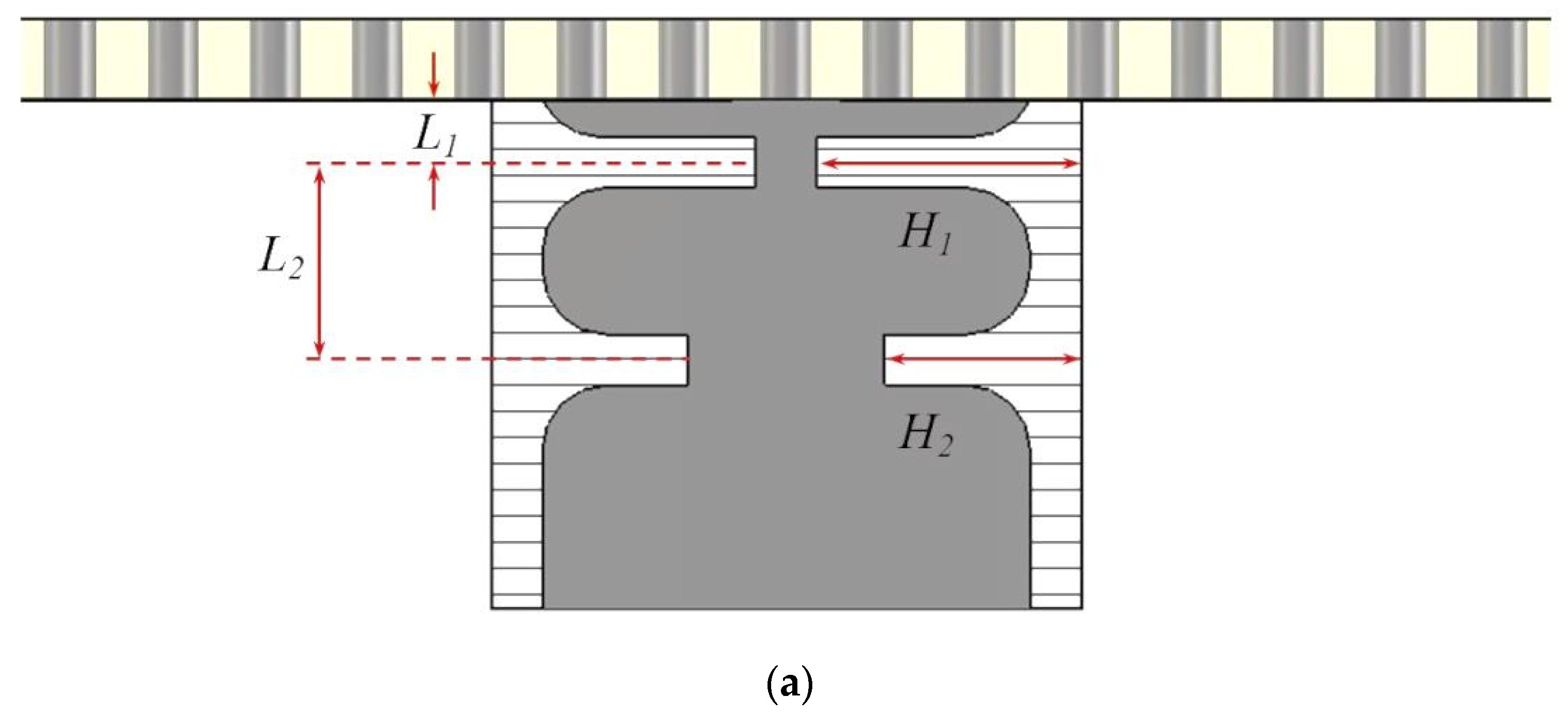
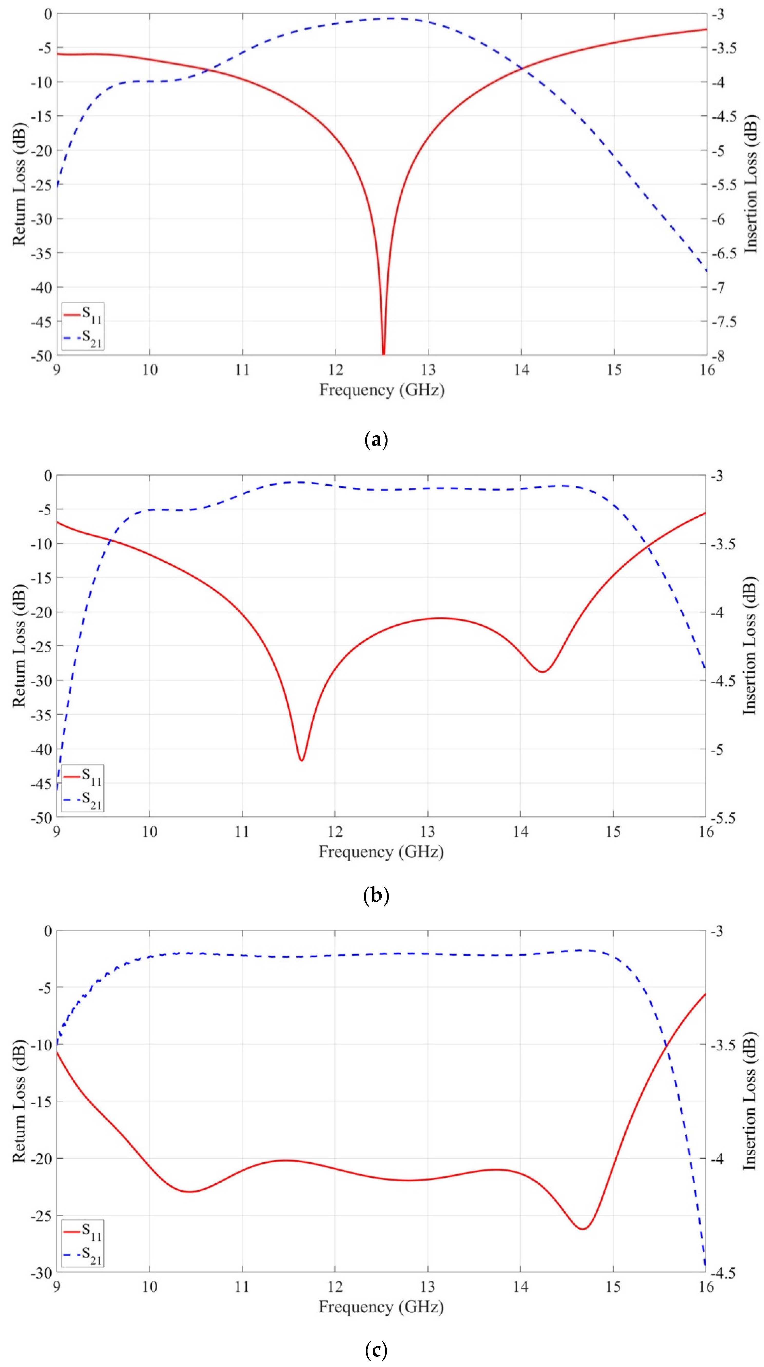
2. Power Divider Design
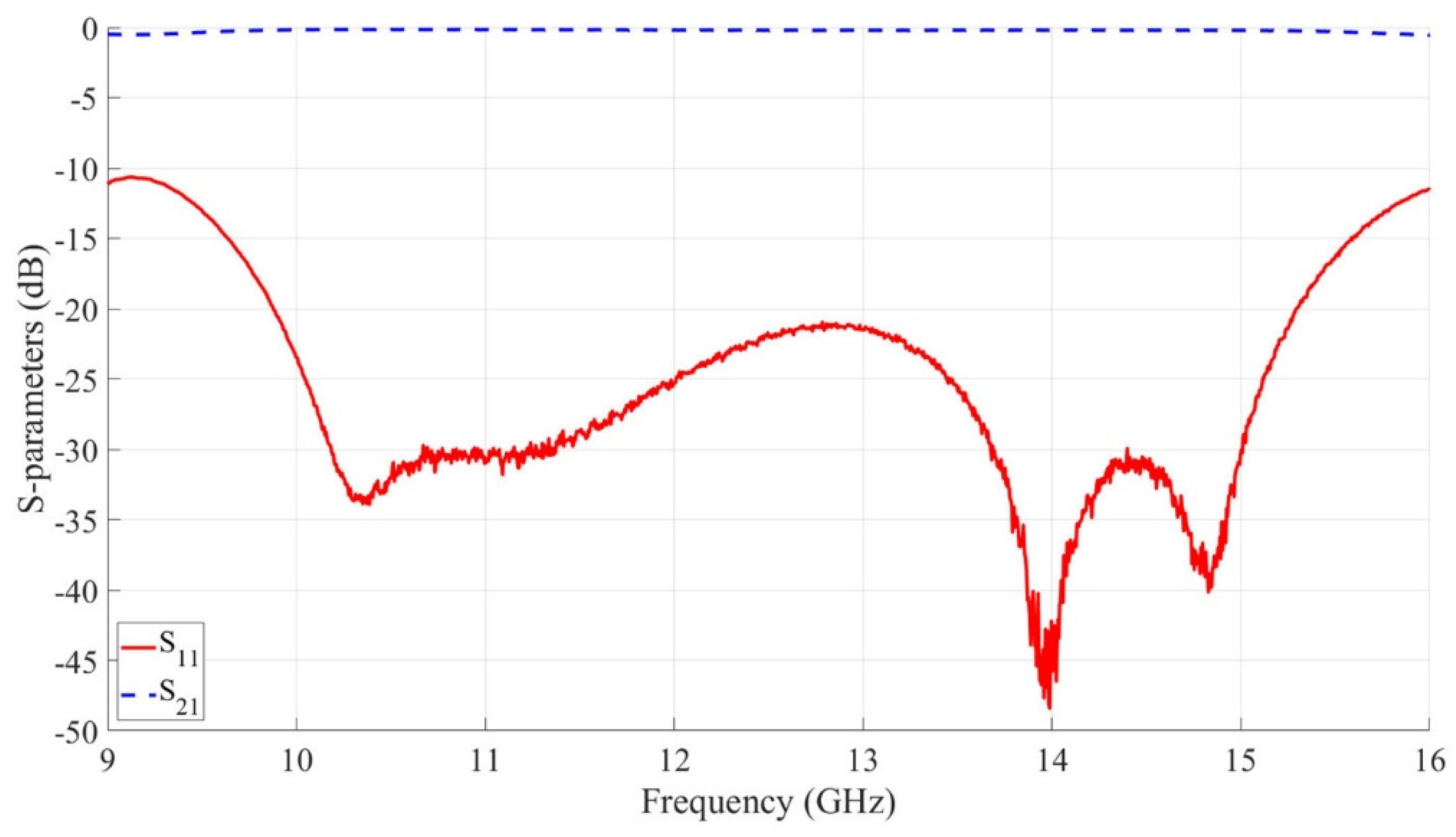
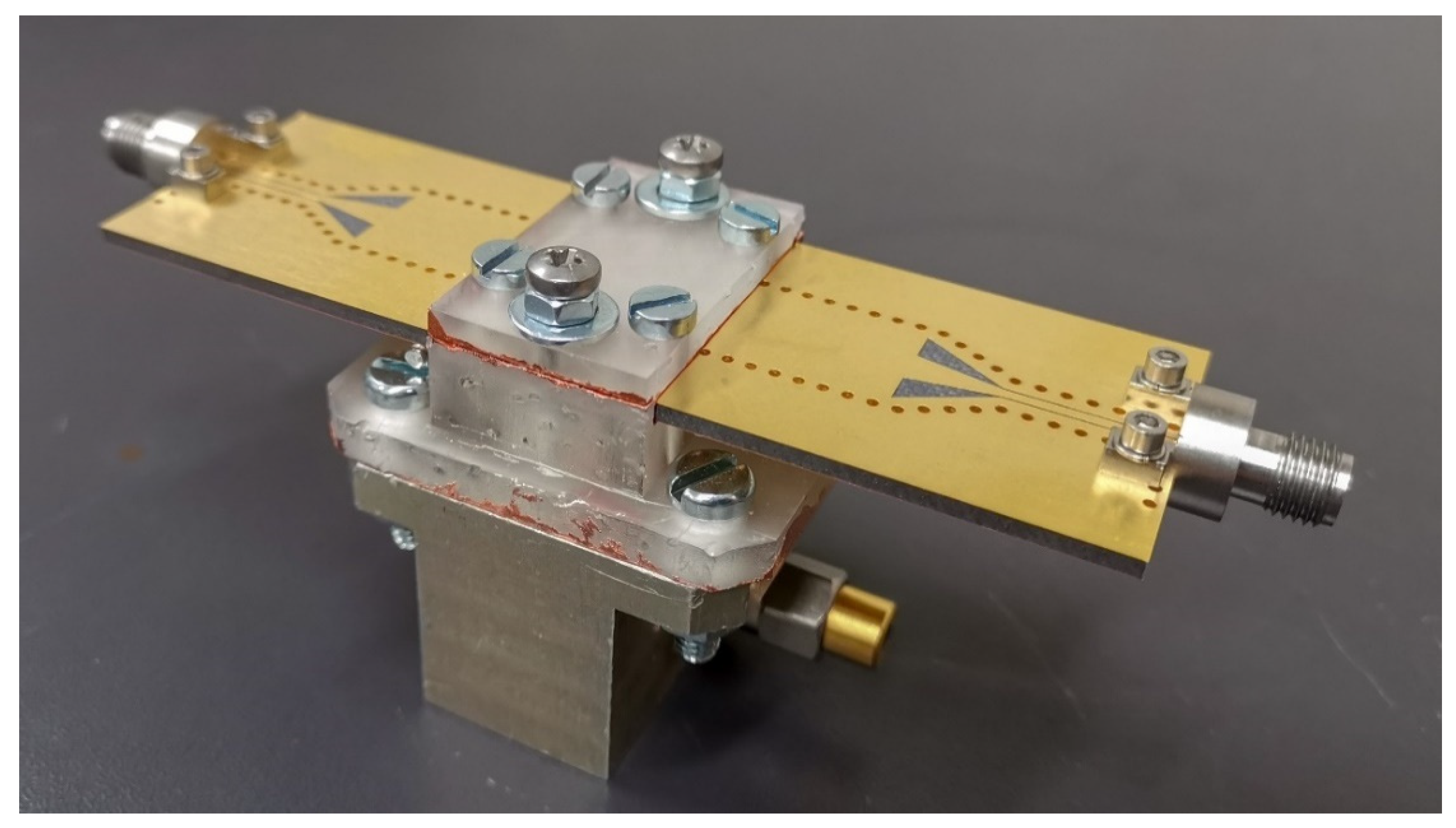
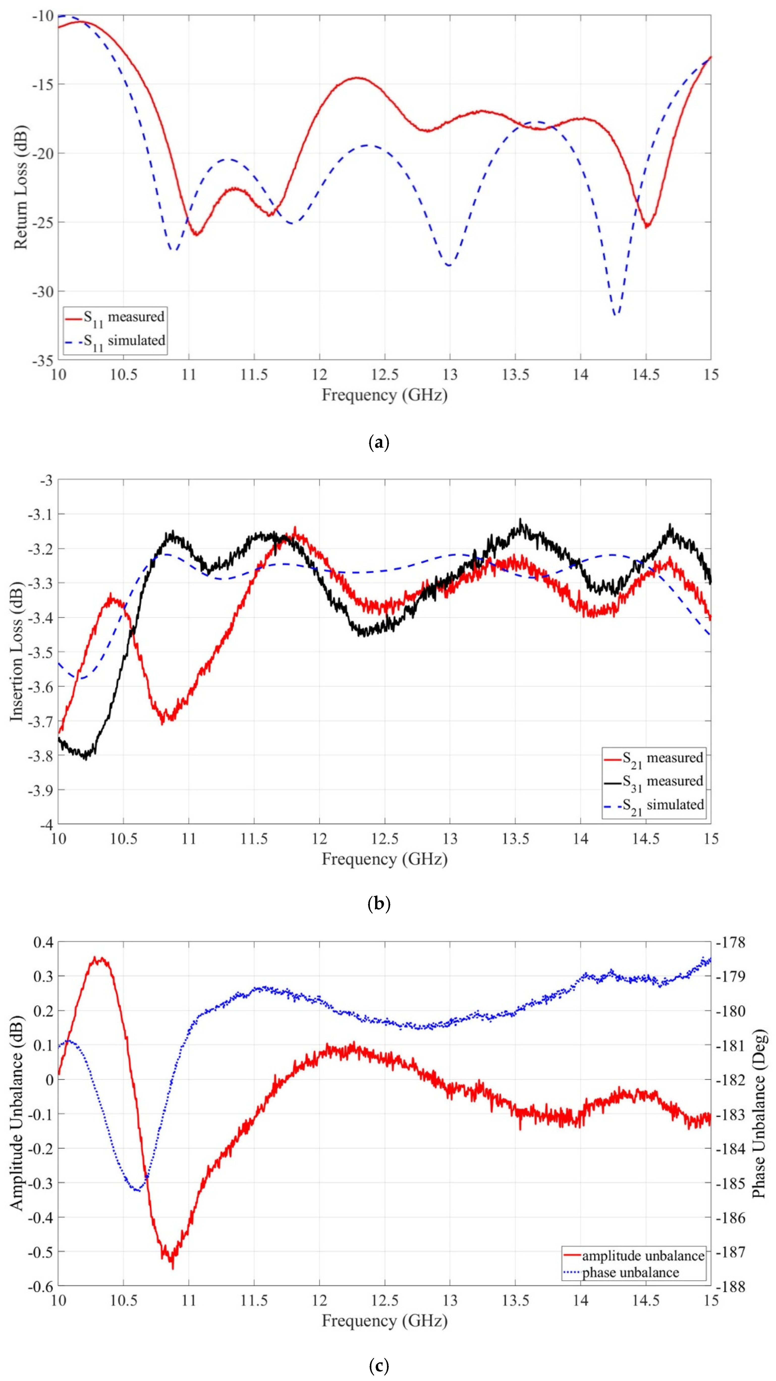
3. Power Divider Manufacturing and Test
4. Conclusions
Author Contributions
Funding
Informed Consent Statement
Data Availability Statement
Conflicts of Interest
References
- Vincenti Gatti, R.; Marcaccioli, L.; Sbarra, E.; Sorrentino, R. Flat Array Antennas for Ku-Band Mobile Satellite Terminals. In Proceedings of the 5th European Conference on Antennas and Propagation (EUCAP), Rome, Italy, 11–15 April 2011; pp. 2618–2622. [Google Scholar]
- Deslandes, D.; Wu, K. Integrated microstrip and rectangular waveguide in planar form. IEEE Microw. Wirel. Components Lett. 2001, 11, 68–70. [Google Scholar] [CrossRef]
- Deslandes, D.; Wu, K. Single-substrate integration technique of planar circuits and waveguide filters. IEEE Trans. Microw. Theory Tech. 2003, 51, 593–596. [Google Scholar] [CrossRef]
- Zhang, Q.; Lu, Y. E-band “T” shape transitions between substrate integrated waveguide and standard waveguide. In Proceedings of the Asia-Pacific Microwave Conference, Macau, China, 16–20 December 2008; pp. 1–4. [Google Scholar]
- Abdel-Wahab, W.; Al-Saedi, H.; Safavi-Naeini, S. E-plane RWG-to-SIW Transition Power Splitter for Ka-Band SATCOM Application. In Proceedings of the IEEE International Symposium on Antennas and Propagation and USNC/URSI National Radio Science Meeting, San Diego, CA, USA, 9–14 July 2017; pp. 2251–2252. [Google Scholar]
- Li, C.; Wu, D.; Seo, K. Rectangle waveguide to substrate integrated waveguide transition and power divider. Microw. Opt. Technol. Lett. 2010, 52, 375–378. [Google Scholar] [CrossRef]
- Bu, S.; Jin, H.; Wang, W.; Luo, G.; Chin, K.-S. A Millimeter-Wave Broadband Transition of Air-Filled Rectangular Waveguide to Differential Substrate Integrated Waveguide. In Proceedings of the IEEE MTT-S International Wireless Symposium (IWS), Guangzhou, China, 19–22 May 2019; pp. 1–3. [Google Scholar]
- Yan, L.; Hong, W.; Wu, K.; Cui, T. Investigations on the propagation characteristics of the substrate integrated waveguide based on the method of lines. IEE Proc. Microwaves Antennas Propag. 2005, 152, 35–42. [Google Scholar] [CrossRef]
- Vincenti Gatti, R.; Dionigi, M.; Sorrentino, R. Low cost active scanning antenna for mobile satellite terminals. In Proceedings of the IEEE Antennas and Propagation Society International Symposium, Columbus, OH, USA, 22–27 June 2004; pp. 680–683. [Google Scholar]
- Pozar, D.M. Microwave Engineering, 4th ed.; John Wiley & Sons: Hoboken, NJ, USA, 2011. [Google Scholar]
- Collin, R.E. Foundations for Microwave Engineering, 2nd ed.; IEEE: Hoboken, NJ, USA, 2000. [Google Scholar]
- Vincenti Gatti, R.; Rossi, R.; Dionigi, M. Broadband Right-Angle Rectangular Waveguide to Substrate Integrated Waveguide Transition with Distributed Impedance Matching Network. Appl. Sci. 2019, 9, 389. [Google Scholar] [CrossRef]
- Dionigi, M.; Tomassoni, C.; Venanzoni, G.; Sorrentino, R. Simple high-performance metal-plating procedure for stereolitho-graphically 3-d-printed waveguide components. IEEE Microw. Wireless Comp. Lett. 2017, 27, 953–955. [Google Scholar] [CrossRef]
- Vincenti Gatti, R.; Rossi, R.; Dionigi, M. X-band right-angle coaxial-to-single ridge waveguide compact transition with capacitive coupling. Electron. Lett. 2019, 55, 103–105. [Google Scholar] [CrossRef]
- Vincenti Gatti, R.; Rossi, R.; Dionigi, M. In-line stepped ridge coaxial-to-rectangular waveguide transition with capacitive coupling. Int. J. RF Microw. Comp.-Aid. Eng. 2019, 29, e21626. [Google Scholar] [CrossRef]
- Vincenti Gatti, R.; Rossi, R.; Dionigi, M.; Spigarelli, A. An x-band compact and low-profile waveguide magic-t. Int. J. RF Microw. Comp.-Aid. Eng. 2019, 29, e21854. [Google Scholar] [CrossRef]
- Kazemi, R.; Fathy, A.E.; Yang, S.; Sadeghzadeh, R.A. Development of an ultra wide band GCPW to SIW transition. In Proceedings of the IEEE Radio and Wireless Symposium, Santa Clara, CA, USA, 15–18 January 2012; pp. 171–174. [Google Scholar]
- Vincenti Gatti, R.; Rossi, R. Hermetic Broadband 3-dB Power Divider/Combiner in Substrate-Integrated Waveguide (SIW) Technology. IEEE Trans. Microw. Theory Tech. 2018, 66, 3048–3054. [Google Scholar] [CrossRef]


| Parameter | Description | Value (mm) |
|---|---|---|
| a | SIW width | 12.500 |
| ae | Equivalent RWG width | 11.865 |
| d | Via hole diameter | 1.000 |
| p | Via hole pitch | 2.000 |
| y | Substrate height | 1.575 |
| t | Metal thickness | 0.045 |
| sl | Slot length (vertical) | 10.350 |
| sh | Slot length (horizontal) | 3.300 |
| sw | Slot width | 2.100 |
| wa | RWG width | 19.050 |
| wb | RWG height | 9.525 |
| Iris Height (mm) | C (pF) | L (pH) | θ (deg) |
|---|---|---|---|
| 0.50 | 1.776 | 314.162 | −0.512 |
| 1.00 | 3.838 | 165.103 | −1.526 |
| 1.50 | 6.438 | 100.696 | −2.192 |
| 2.00 | 10.131 | 63.611 | −2.765 |
| 2.50 | 14.894 | 44.643 | −3.374 |
| 3.00 | 22.089 | 29.057 | −4.039 |
| 3.50 | 31.240 | 22.417 | −4.537 |
| 4.00 | 49.427 | 14.315 | −5.198 |
| 4.50 | 110.015 | 6.473 | −5.883 |
| Interpolation Coefficients | |||
|---|---|---|---|
| c3 | c2 | c1 | c0 |
| 1.364 | −6.294 | −4.894 | −4.044 |
| l3 | l2 | l1 | l0 |
| −12.950 | 126.500 | −413.900 | 482.100 |
| t3 | t2 | t1 | t0 |
| −0.051 | 0.428 | −2.319 | 0.503 |
| Parameter | Description | Design 1 Value (mm) | Design 2 Value (mm) | Design 3 Value (mm) |
|---|---|---|---|---|
| H1 | First iris height | 3.393 | 3.907 | 4.050 |
| H2 | Second iris height | - | 2.525 | 3.318 |
| H3 | Third iris height | - | - | 1.931 |
| L1 | First iris distance | 2.360 | 1.793 | 1.565 |
| L2 | Second iris distance | - | 4.661 | 3.836 |
| L3 | Third iris distance | - | - | 5.654 |
| Parameter | Description | Design 1 Value (mm) | Design 2 Value (mm) | Design 3 Value (mm) |
|---|---|---|---|---|
| H1 | First iris height | 3.647 | 4.160 | 4.212 |
| H2 | Second iris height | - | 2.837 | 3.414 |
| H3 | Third iris height | - | - | 1.667 |
| L1 | First iris distance | 2.064 | 1.209 | 1.237 |
| L2 | Second iris distance | - | 3.887 | 3.494 |
| L3 | Third iris distance | - | - | 5.674 |
| Reference | [4] | [5] | [6] | [7] | This Work (1) | This Work (2) | This Work (3) |
|---|---|---|---|---|---|---|---|
| f0 (GHz) | 78.60 | 29.85 | 12.53 | 32.25 | 12.50 | 12.83 | 12.48 |
| εr | 2.20 | 3.55 | 2.20 | 2.20 | 2.20 | 2.20 | 2.20 |
| a (mm) | 2.24 | 4.80 | 11.00 | 4.80 | 12.50 | 12.50 | 12.50 |
| y (mm) | 0.787 | 0.787 | 1.000 | 0.787 | 1.575 | 1.575 | 1.575 |
| ae (mm) | 2.00 | 4.54 | 10.36 | 4.60 | 11.87 | 11.87 | 11.87 |
| λc (mm) | 5.93 | 17.11 | 30.73 | 13.65 | 35.21 | 35.21 | 35.21 |
| r (%) | 13.26 | 4.60 | 3.25 | 5.76 | 4.47 | 4.47 | 4.47 |
| BW20dB (MHz) | 9880 | 701 | 350 | 11,500 | 810 | 3707 | 5108 |
| FBW (%) | 12.57 | 2.35 | 2.79 | 35.66 | 6.48 | 28.89 | 40.93 |
| F | 0.95 | 0.51 | 0.86 | 6.18 | 1.45 | 6.45 | 9.15 |
| F/F [7] | 0.15 | 0.08 | 0.14 | 1.00 | 0.23 | 1.04 | 1.48 |
| Parameter | Description | Value (mm) |
|---|---|---|
| w1 | GCPW initial width | 1.000 |
| w2 | GCPW final width | 3.530 |
| g1 | GCPW initial gap | 0.180 |
| g2 | GCPW final gap | 3.157 |
| L | Taper length | 7.387 |
| x | Line-via distance | 2.180 |
Publisher’s Note: MDPI stays neutral with regard to jurisdictional claims in published maps and institutional affiliations. |
© 2021 by the authors. Licensee MDPI, Basel, Switzerland. This article is an open access article distributed under the terms and conditions of the Creative Commons Attribution (CC BY) license (http://creativecommons.org/licenses/by/4.0/).
Share and Cite
Vincenti Gatti, R.; Rossi, R.; Dionigi, M. Wideband Rectangular Waveguide to Substrate Integrated Waveguide (SIW) E-Plane T-Junction. Electronics 2021, 10, 264. https://doi.org/10.3390/electronics10030264
Vincenti Gatti R, Rossi R, Dionigi M. Wideband Rectangular Waveguide to Substrate Integrated Waveguide (SIW) E-Plane T-Junction. Electronics. 2021; 10(3):264. https://doi.org/10.3390/electronics10030264
Chicago/Turabian StyleVincenti Gatti, Roberto, Riccardo Rossi, and Marco Dionigi. 2021. "Wideband Rectangular Waveguide to Substrate Integrated Waveguide (SIW) E-Plane T-Junction" Electronics 10, no. 3: 264. https://doi.org/10.3390/electronics10030264
APA StyleVincenti Gatti, R., Rossi, R., & Dionigi, M. (2021). Wideband Rectangular Waveguide to Substrate Integrated Waveguide (SIW) E-Plane T-Junction. Electronics, 10(3), 264. https://doi.org/10.3390/electronics10030264