Article

Analysis of the Resonator Part of a Ka-Band Multiple-Beam Extended-Interaction Oscillator through Electric Field Uniformity

School of Electronic Science and Engineering, Shahe Campus, University of Electronic Science and Technology of China, Chengdu 610054, China
*
Author to whom correspondence should be addressed.
Electronics 2021, 10(3), 276; https://doi.org/10.3390/electronics10030276
Submission received: 16 December 2020 / Revised: 8 January 2021 / Accepted: 21 January 2021 / Published: 25 January 2021
(This article belongs to the Special Issue Microwave Devices Design and Application)

Abstract

:
The development of multiple-beam devices is required due to the increasing demand of compact, high-frequency, and high-power vacuum devices. A Ka-band multiple-beam extended-interaction oscillator which operates in TM01 mode with a large diameter (as the value is 14.6 mm which is larger than the operating wavelength of 8 mm) to obtain high output power has been put forward. In previous studies, the performance differences of single-beam extended-interaction oscillator with different electric field uniformity can be as high as 70%. Simulation results predicted the multiple-beam device has an average output power of 7.594 kW when a total beam of 3 A, 18 kV and the uniformity parameter is 0.064. Meanwhile, it predicted that the difference of output power of multiple-beam devices with different field uniformity (corresponding uniformity parameter is within 0.064~0.278) is within 2.53% when other operating conditions are unchanged. The results show that the multiple-beam device substantially decreases the influence of the field uniformity, which is an important factor for the performance in the single-beam device. A cold test experiment has been carried out based on perturbation theory to obtain the electric field distribution curves of this device, and this provides a method for studying multiple-beam devices.

1. Introduction

The development of an electronic vacuum device involves obtaining high power and operating in high frequency [1,2,3,4,5]. Extended-interaction oscillator (EIO) is one kind of electronic vacuum device. EIO combines the advantages of the slow-wave circuit and the coupled cavity to achieve high output power, efficient beam-wave interaction, and reliability; meanwhile, it can also be miniaturized [6,7,8,9]. The output power of EIO depends on the current which can be transported through the device at a particular voltage [10]. The previous design schemes involve designing the multiple electron-beams which are parallel-arrayed between the coupling cavities [9,11]. Meanwhile, the fact that dimension of the device becomes smaller with the increasing frequency must be taken into consideration. The width of the sheet beam cannot be further enlarged due to the problems of field distribution uniformity and mode competition while devices operate in W-band and higher. The previous scheme made EIOs operate in higher order mode so that the efficiency of wave interaction would be lower than that of the basic mode under the same operating condition [11,12,13]. Thus, our team has designed a multiple-beam extended-interaction oscillator (MBEIO) with a large diameter (as the value is 14.6 mm which is larger than the operating wavelength of 8 mm) which operates in TM mode [14,15].
The electric field uniformity of MBEIO is a noteworthy parameter as it is an important parameter for the performance but has not been analyzed in the previous studies [16,17]. In this paper, the output power of MBEIOs which have different electric field distribution uniformity have been predicted by simulation with Computer-Simulation-Technology (CST) microwave studio. The uniformity parameter value is employed to quantify the uniformity of the electric field distribution, and its calculation method has been presented in the next section. The simulation results show that the multiple-beam device with a large diameter substantially decreases the influence of the field uniformity which is an important factor for the performance in the single-beam device [18].
The previous measurement methods which are suitable for the device with operating frequency less than 26.5 GHz are no longer applicable for the MBEIO. Thus, a measurement scheme based on perturbation theory is provided to obtain the uniformity parameter value in this paper. Perturbation theory is generally used to measure dielectric constant of materials and the change in the resonant frequency of devices [19,20,21,22,23,24,25]. The most common perturbation methods include changing device structures and changing filling mediums [20]. Changing filling mediums have been employed in this study because of advantages such as being non-destructive, flexible, and high-precision. The electric field distribution uniformity of the MBEIO has been obtained in the experiment.

2. Analysis and Simulation

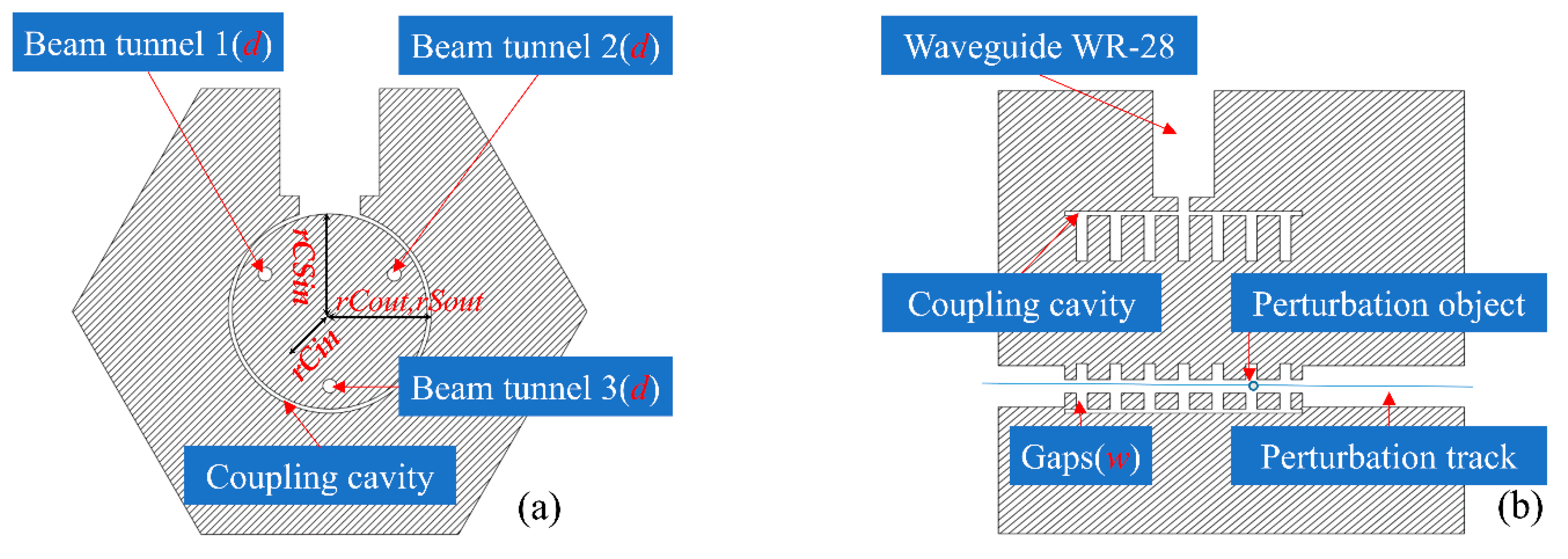
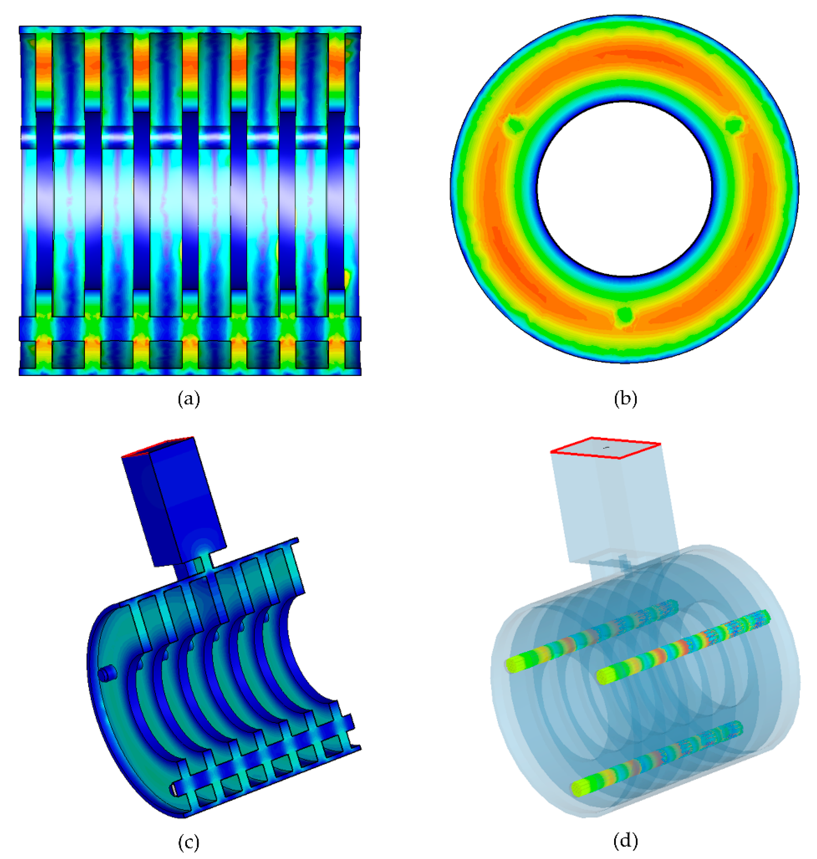
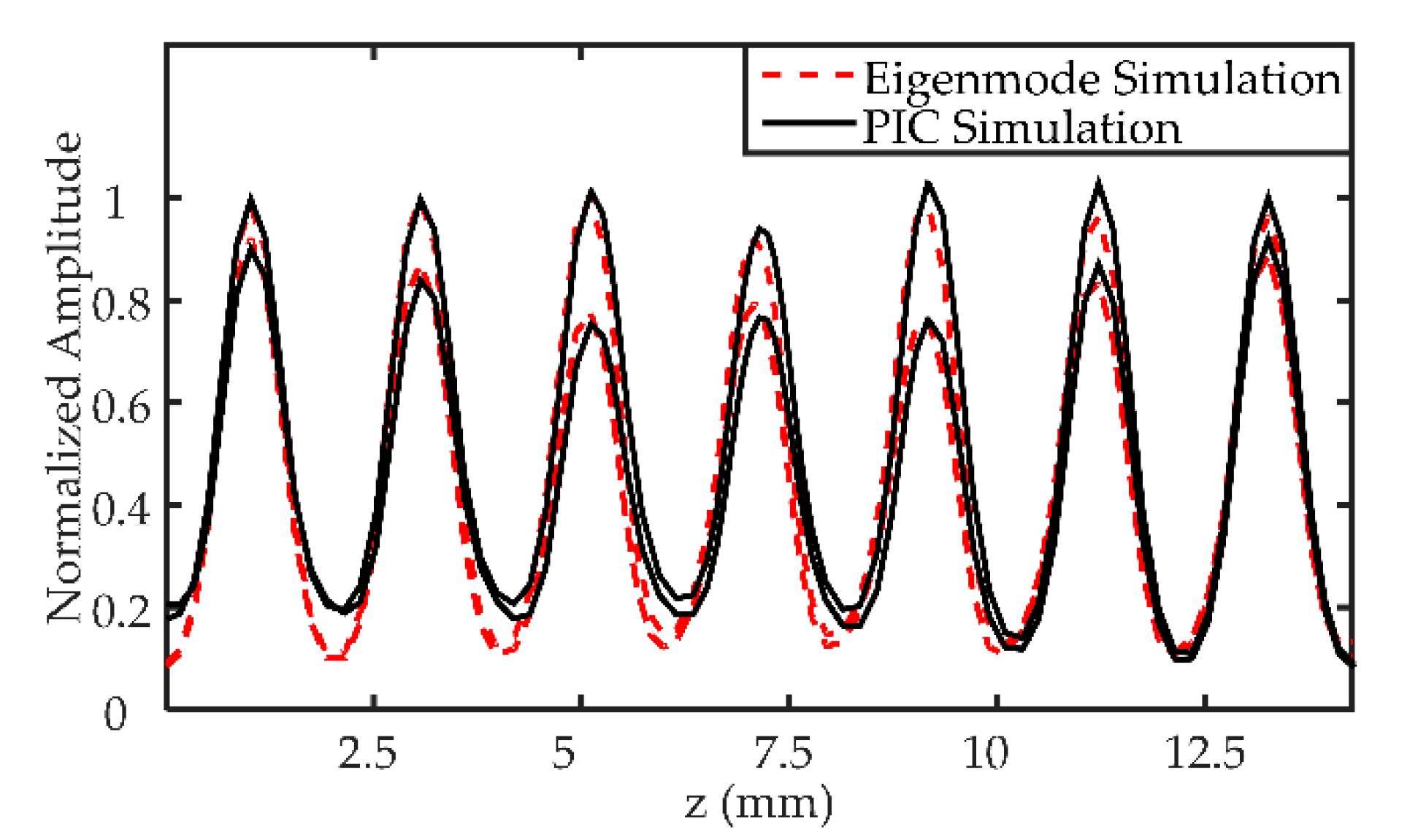
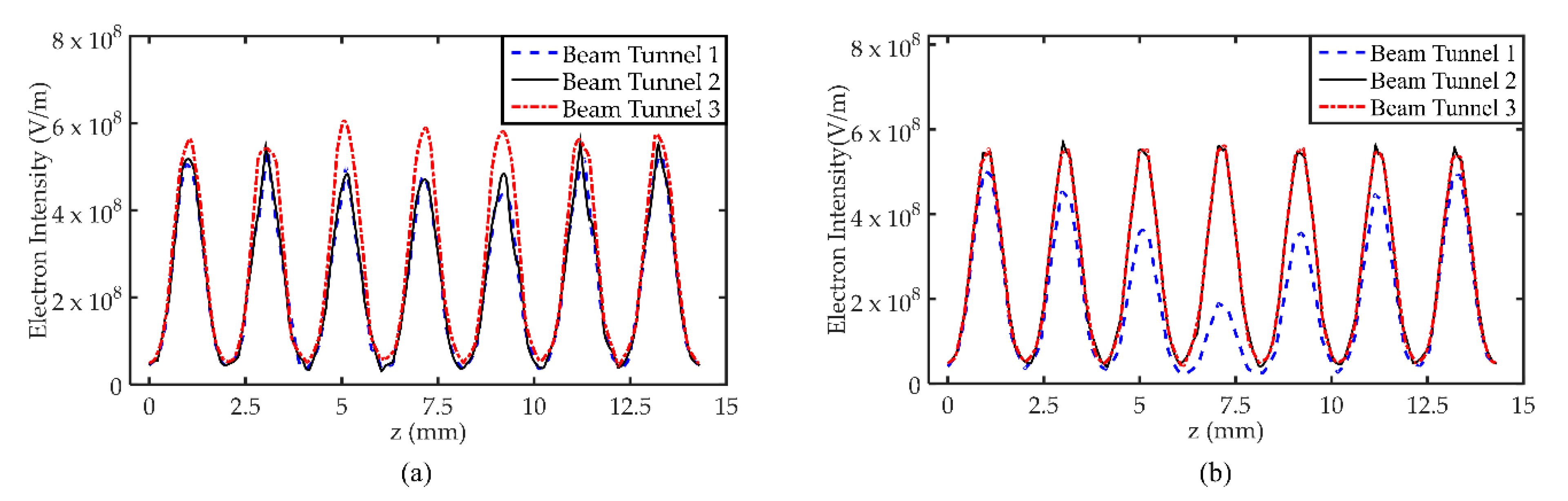
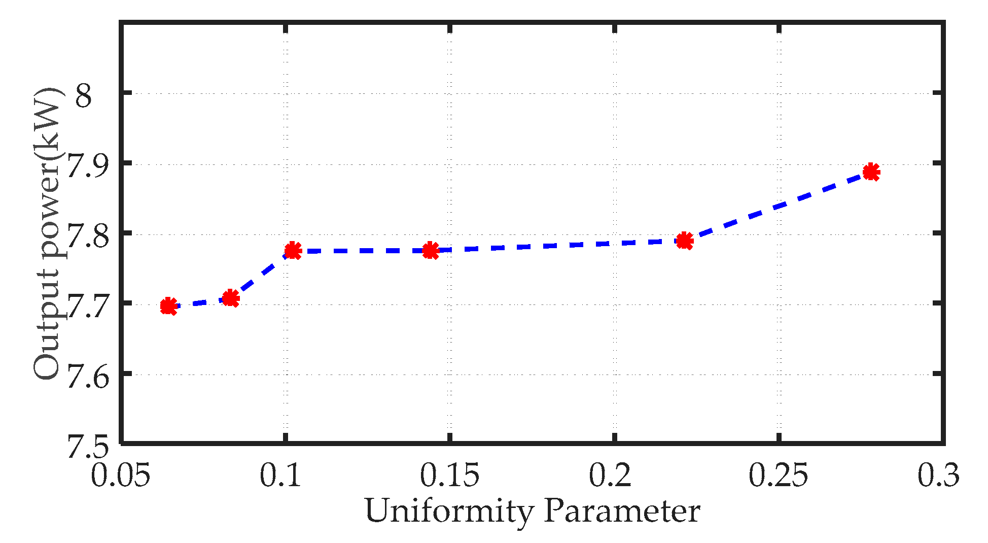
2.1. Analysis of Field Uniformity

This designed MBEIO is based on our previous study of the five-beams EIO [14]. The MBEIO circuit consists of three beam tunnels, an annular closed coupling cavity and seven interaction gaps. As shown in Figure 1, the device which corresponds to this circuit is named ‘device-0’ for the convenience of understanding and set as the studying object. The specific parameter values of MBEIO circuit have been given in Table 1.
Figure 2a,b show the eigenmode electric field contour in the 2π mode with seven periods. Figure 2c shows the field distribution of this MBEIO agrees well with the eigenmode simulation. Figure 2d shows a snapshot of the 3-D trajectory of the electrons within the device after oscillation, and a clear bunching of the electrons has been obtained. Figure 3 shows that the stable output power of device-0 is 7.594 kW and the operating frequency is 35.36 GHz. The changing of output power with operating voltage is shown in Figure 4 and the 18 kV is chosen to be the operating voltage as it corresponds to the highest output power.
Figure 5 shows the comparison of field distribution curves between eigenmode simulation and PIC (particle-in-cell) simulation. Corresponding field distributions of the two are basically the same; thus, the field distribution under the eigenmode can be used to predict the device performance.
The electric field uniformity of MBEIO will be changed with the changing structure of the device. The uniformity parameter which is selected for studying the uniformity is calculated by the following steps. Firstly, the field intensity value at the center point of each cycle on the axis line of each beam tunnel are obtained by simulation and experiment so that seven sets of data can be obtained, and each set contains three pieces of data. Secondly, the average value of each set of data is calculated and selected as the reference value, and the three data are normalized based on it. Thirdly, the variance of each set of normalized data is calculated, and the results are added to obtain the uniformity parameter value. According to the above method, the uniformity parameter values of several devices are calculated and shown in Table 2.
The field intensity curves of device-0 and device-5 are shown in Figure 6, respectively. By comparing the corresponding field intensity curves of the device-0 and device-5, it can be concluded that the smaller the uniformity parameter value is, the better the field distribution uniformity. Figure 7 shows that the output power is affected slightly with the uniformity parameter and keep a relatively stable state. Therefore, it could be concluded that the multiple-beam extended-interaction oscillator substantially decreases the influence of electric field uniformity, which is an important parameter for performance in single-beam extended-interaction oscillator. The next section presents a method for measuring field uniformity in order to further study the effect of field uniformity on device performance in practical applications.

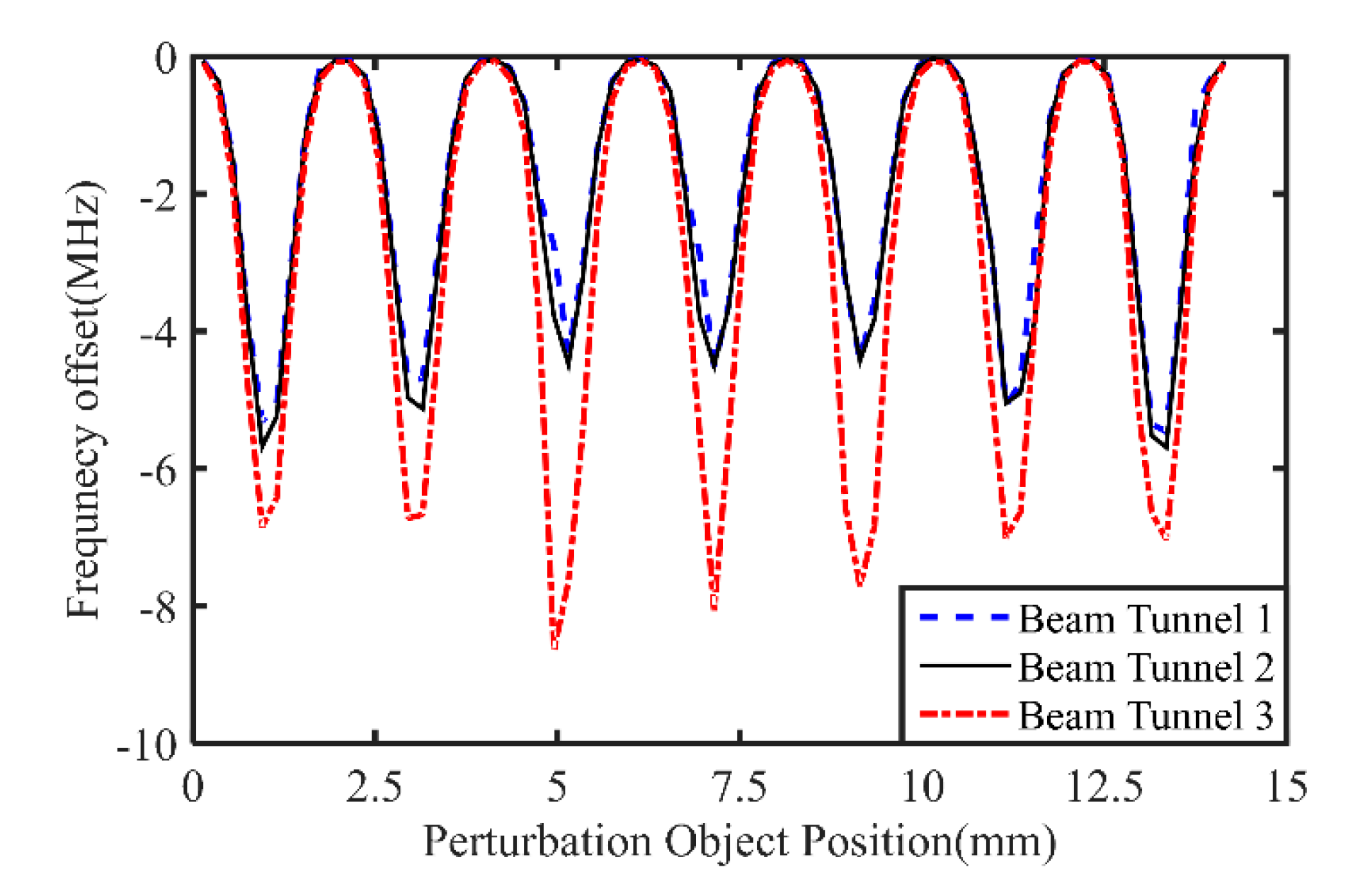
2.2. Analysis Based on Perturbation Theory

It is extremely difficult to obtain the electric field intensity of the axial line of a resonator by experiments; thus, the frequency offset parameter is chosen as the experimental measuring object. Dielectric perturbation theory is employed to obtain the intensity of the electric field. The insulator ball which has a radius of 0.325 mm and the dielectric constant of 4.82 is employed as the perturbation object and the related resonator perturbation expression is given below (1), as already reported in [26]:
Δ f f 0 = f f 0 f 0 V 0 Δ E D 0 ¯ E 0 ¯ Δ D + Δ H B 0 ¯ H 0 ¯ Δ B d v V 0 E 0 ¯ D 0 + H 0 ¯ B 0 d v
In the relation, f0 and f are the frequency of the resonator with or without perturbation object, respectively. V0 is the volume of the resonator cavity. When the perturbation object is not added in the resonator cavity, E0 and D0 are the electric field vector, induction intensity vector, respectively, and E 0 ¯ and D 0 ¯ are the corresponding conjugate complex numbers; H0 and B0 are magnetic field vector, magnetic induction intensity vector, respectively, and H 0 ¯ and B 0 ¯ are the corresponding conjugate complex numbers. Values of Δ H and Δ B are 0 due to that the perturbation of dielectric medium of the magnetic field is negligible.
The field intensity inside the dielectric perturbation object can be regarded as uniform when the size of three axes is far less than the wavelength, and the influence of the change in the field intensity inside the perturbation object on the frequency migration of the whole resonator cavity is negligible. Based on the above theory, the perturbation expression in the ellipsoid coordinate system has been studied and is given below (2) [20]:
Δ f f 0 = f f 0 f 0 1 ε r 1 + abc 2 ε r 1 A 4 3 π abc ε 0 E 0 E 0 ¯ 4 W
In this relation, a, b, c are the dimensional values of the perturbation object. W is the energy storage of cavity. ε is dielectric constant of perturbation object, ε r is relative dielectric, and ε 0 can be calculated with expression 3 which is given below (3):
ε = ε r ε 0
The dielectric sphere is chosen as the perturbation object on account of the consideration of the reliability and feasibility of the experimental scheme. In the spherical coordinates, the express (2) has been further derived to obtain the corresponding perturbation expression which is given below (4):
Δ f f 0 = 3 1 ε r 2 + ε r ε 0 E 0 E 0 ¯ 4 W 4 3 π a 3
The frequency offset value is proportional to the square value of electric field intensity according to Formula (4).
The frequency that can be disturbed by the perturbation object is very small because the frequency offset value is less than 10 MHz. Thus, a vacuum perturbation object with the same dimension is added at the same position to obtain more accurate simulation results as it can exclude the frequency offset caused by the changing of grid, and the frequency corresponding to TM01 mode of this device serves as the reference frequency f0. Figure 8a shows simulated S11 parameters at the standard waveguide port. Figure 8b shows the frequency with dielectric perturbation object at 2π mode. Figure 8c shows the frequency with vacuum perturbation object at 2π mode. The frequency offset value of 5.5 MHz can be obtained by comparing the 2π mode operating frequency. Seventy sets of simulations based on the described perturbation theory have been carried out and corresponding results are shown in Figure 9. The calculated uniformity parameter value is 0.069 based on the method mentioned in Part A of Chapter 1 and Formula (4), and the deviation between the uniformity parameter of the field intensity and the uniformity parameter of frequency offset is 7.8% which is due to the difference in the location of the sampling point. Thus, the measurement scheme is proved to be feasible by simulation.

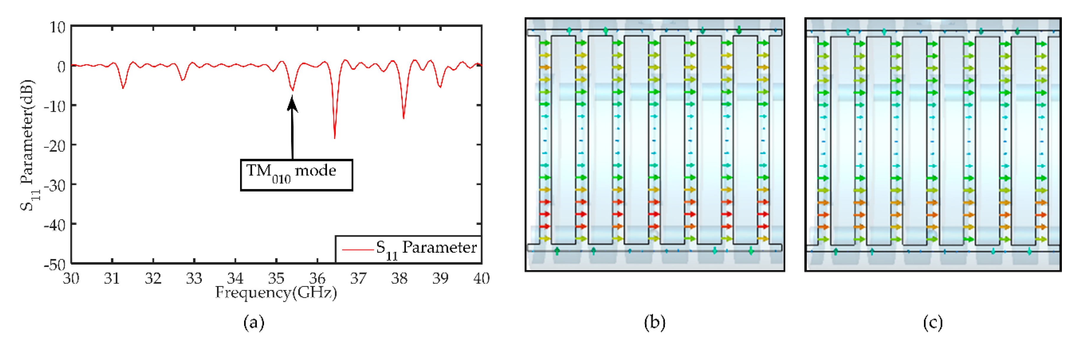
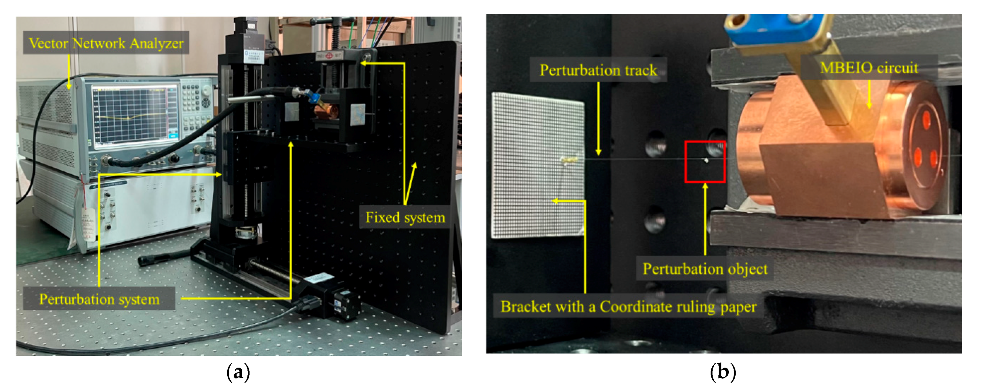
3. Cold Test Experiment

3.1. Schematic of the Measurement Setup

The experimental test platform is shown in Figure 10a, and consists of a Vector Network Analyzer (VNA) system, perturbation system, and the fixed system of MBEIO circuit. The VNA system is employed to measure S11 parameter accurately so that the resonant frequency of MBEIO cavity can be obtained. The specific VNA model is “CEYAER AV3672C” and it was developed and produced by the 41st Institute of Electronic Science and Technology of China [27]. The perturbation system consists of a dielectric perturbation object, a perturbation track, two optical brackets and electronically controlled displacement plat form. Thus, the perturbation object can make accurate displacement in the electronic beam tunnel, and the bit shift step length is 0.2 mm in this experiment. The schematic diagram of the partial perturbation system and the connection scheme of each part are shown in Figure 10b. The fixed system of MBEIO circuit, which is employed to ensure that the circuit is in the horizontal position, consists of a clamp and optical plate so as to improve the reliability of the measurement.
In this experiment, the S11 parameter of MBEIO circuit is changed with the perturbation object position and accurately obtained by VNA.

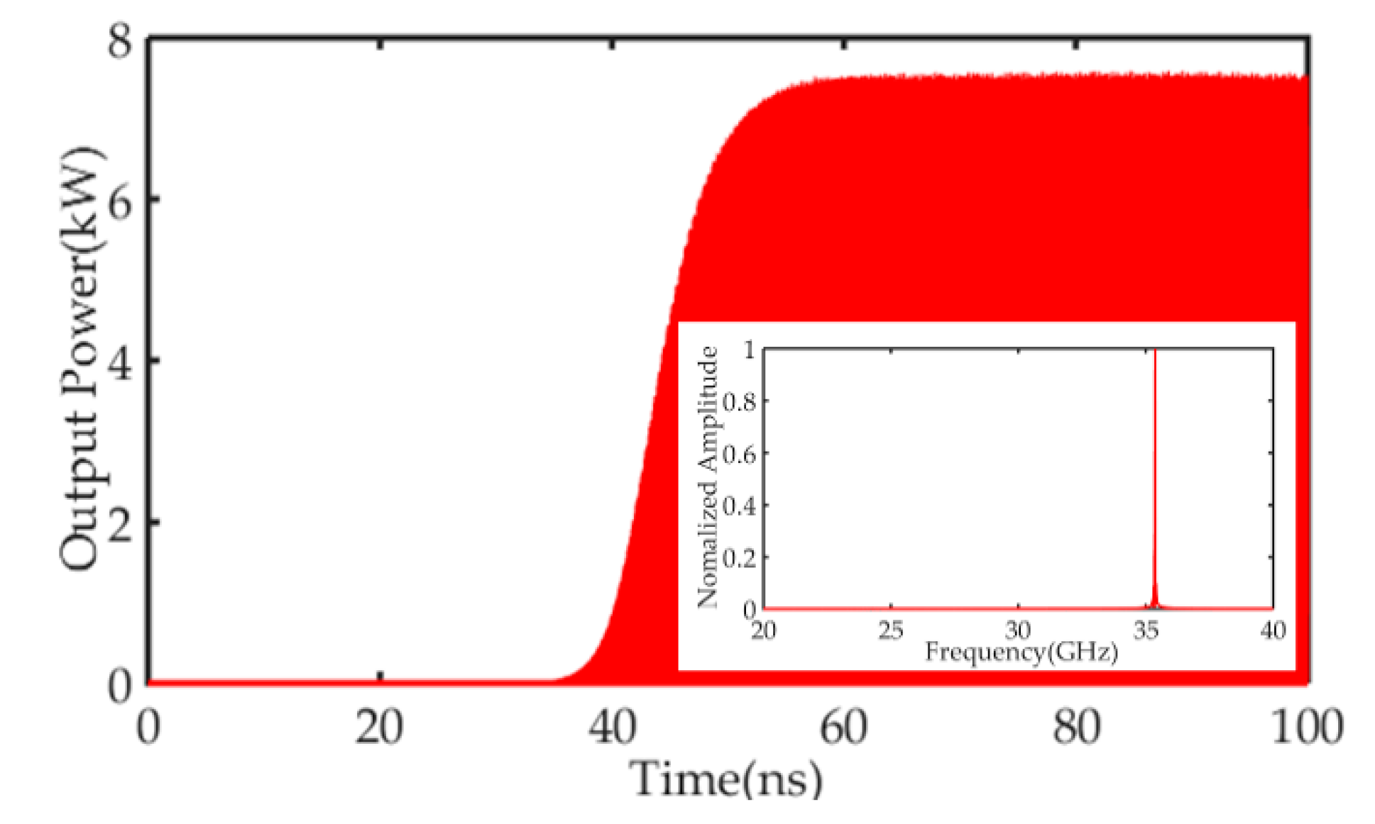
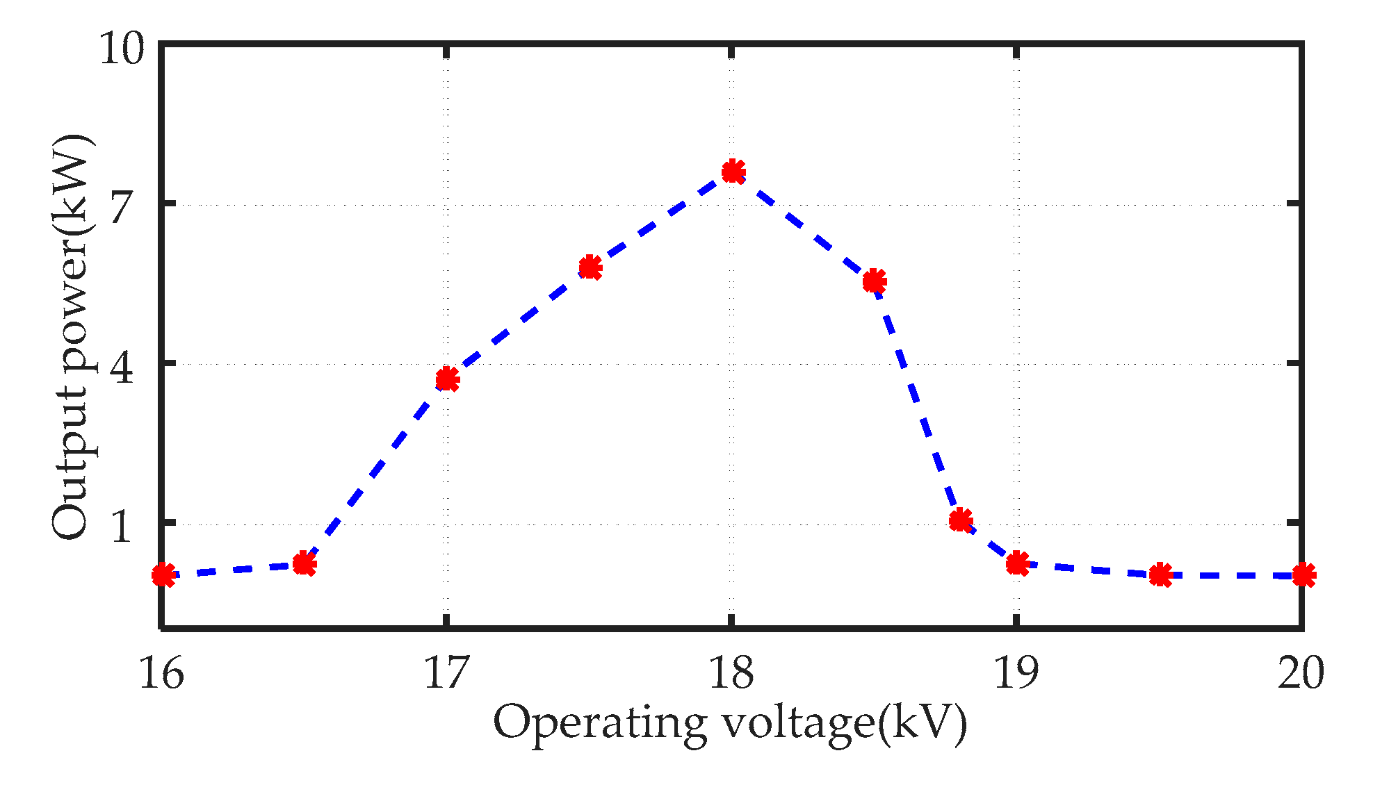
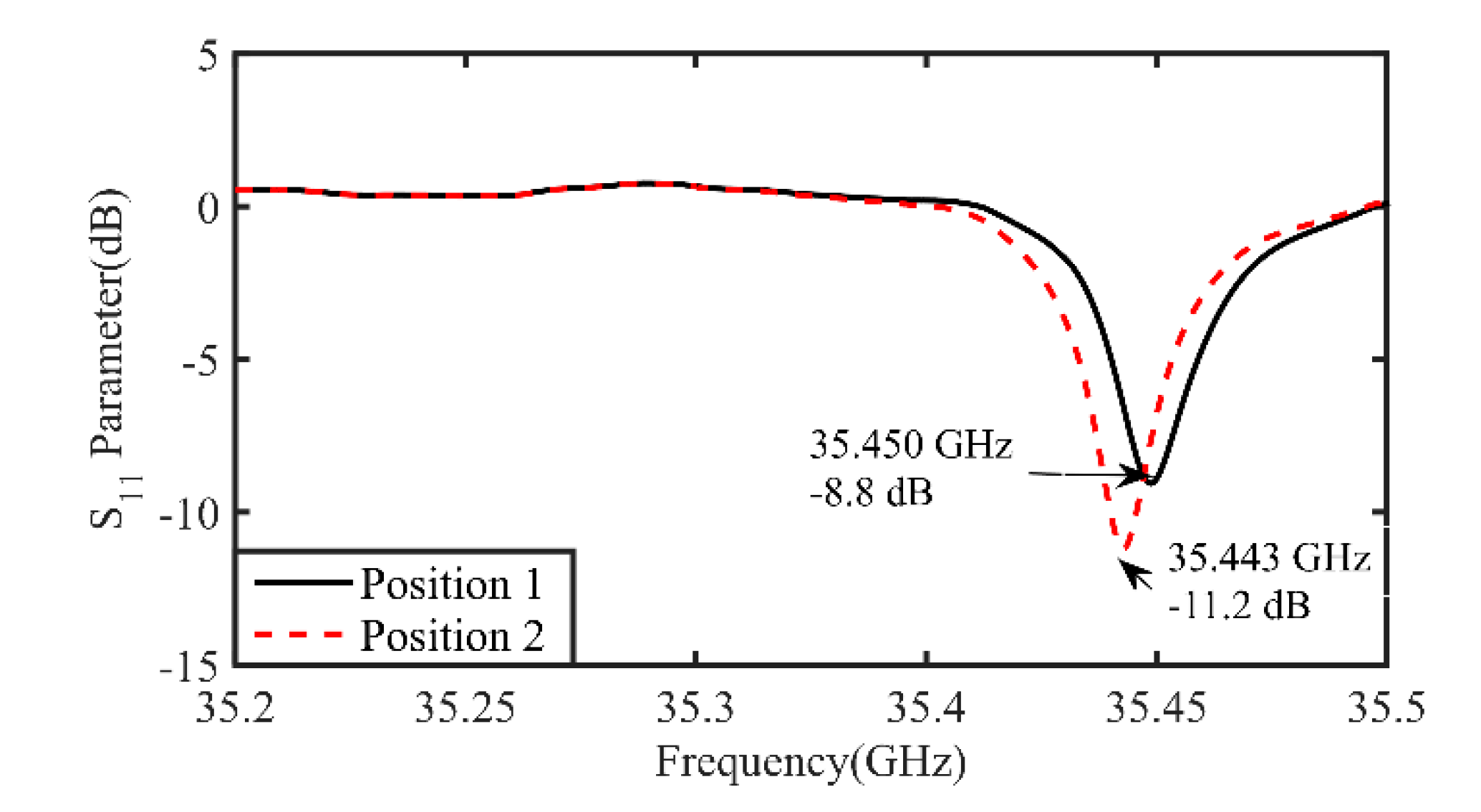
3.2. Analysis of Experimental Results

The 2π mode resonant frequency is changed with the position of the perturbation object, and shown in Figure 11. The frequency offset value depends on the intensity of the electric field at the position of the perturbation object. The position 1 corresponds to the fact that the perturbation object is not located in the beam tunnel, and the resonant frequency of 35.45 GHz is employed as the reference frequency for the experimental data processing. Thus, the perturbation object at position 2 causes a 7 MHz frequency offset.
The frequency offset values measured at the center of each cycle are listed in Table 3. The normalized frequency offset value is proportional to the square of the value of the normalized field intensity based on Formula (3). The experimental uniformity parameter value was calculated to be 0.088, the deviation may be caused by assembly tolerances and machining accuracy. Therefore, it demonstrates that this measurement method could be adopted to study extended-interaction resonant cavities. There are some applications of this method, such as: verifying machining accuracy of cavities, confirming the field distribution corresponding to the resonance points, etc.

4. Conclusions and Discussion

In this paper, the stability of a Ka-band MBEIO has been analyzed through the electric field distribution uniformity. This designed MBEIO could operate stably and has a good performance and it has substantially decreased the influence of electric field uniformity for the device performance. The experiment has been carried out based on perturbation theory, and the experimental uniformity parameter value is 0.088 which is basically consistent with the simulation. This study has greatly enhanced our confidence in the development of MBEIO with a large diameter.
These multiple-beam extended-interaction oscillators with a large diameter which operate in a higher frequency are being studied for their ability to obtain a higher output power and practical application value. We plan to assemble the device to verify it experimentally in the near future.

Author Contributions

Conceptualization, Y.Q. and Y.Y.; methodology, Y.Q. and C.X.; software, Y.Q.; validation, Y.Q.; formal analysis, Y.Q.; investigation, C.X., T.Y. and L.B.; resources, Y.Y.; data curation, Y.Q.; writing—original draft preparation, Y.Q.; writing—review and editing, Y.Q., X.X., J.X. and Y.Y.; visualization, Y.Q. and Q.C.; supervision, Y.Y., B.W., H.L., X.Y. and L.M.; project administration, Y.Y.; funding acquisition, Y.Y. All authors have read and agreed to the published version of the manuscript.

Funding

This research was funded by the National Natural Science Foundation of China (No. 61671116, 61771096, 11905026), National Key Research and Development Program of China (No.2019YFA0210202) and Fundamental Research Funds for the Central Universities (No. ZYGX2019Z006, ZYGX2019J012). (Corresponding author: Yong Yin). The authors are with Vacuum Electronic National Laboratory, School of Electronic Science and Engineering, University of Electronic Science and Technology of China, Chengdu 610054, China. (email: [email protected]).

Conflicts of Interest

The authors declare no conflict of interest.

References

  1. Cui, J.; Bian, S.; Li, A. A Multiobjective Optimization Approach for Extended Interaction Oscillators. IEEE Access 2020, 8, 166226–166235. [Google Scholar] [CrossRef]
  2. Nguyen, T.D.; Hong, J.-P. A 350-GHz Coupled Stack Oscillator with −0.8 dBm Output Power in 65-nm Bulk CMOS Process. Electronics 2020, 9, 1214. [Google Scholar] [CrossRef]
  3. Thanh Dat, N.; Park, H.; Hong, J.-P. A Millimeter-Wave Fundamental Frequency CMOS-Based Oscillator with High Output Power. Electronics 2019, 8, 1228. [Google Scholar]
  4. Booske, J.H.; Dobbs, R.J.; Joye, C.D.; Kory, C.L.; Neil, G.R.; Park, G.; Park, J.; Temkin, R.J. Vacuum Electronic High Power Terahertz Sources. IEEE Trans. Terahertz Sci. Technol. 2011, 1, 54–75. [Google Scholar] [CrossRef]
  5. Shu, G.; Deng, J.; Huang, Z.; Chen, L.; Lin, J.; Hong, B.; He, W. Design and Measurement of a Terahertz Band Rectangular TE20 Mode Power Coupling Structure for High-Order Overmoded Multiple Sheet Electron Beam Devices. IEEE Electron Device Lett. 2020, 41, 920–923. [Google Scholar] [CrossRef]
  6. Berry, D.; Deng, H.; Dobbs, R.; Horoyski, P.; Hyttinen, M.; Kingsmill, A.; MacHattie, R.; Roitman, A.; Sokol, E.; Steer, B. Practical Aspects of EIK Technology. IEEE Trans. Electron Devices 2014, 61, 1830–1835. [Google Scholar] [CrossRef]
  7. Chodorow, M.; Wessel-Berg, T. A high-efficiency klystron with distributed interaction. IEEE Trans. Electron Devices 1961, 8, 44–55. [Google Scholar] [CrossRef]
  8. Chodorow, M.; Kulke, B. An extended-interaction klystron: Efficiency and bandwidth. IEEE Trans. Electron Devices 1966, ED-13, 439–447. [Google Scholar] [CrossRef]
  9. Korolyov, A.N.; Gelvich, E.A.; Zhary, Y.V.; Zakurdayev, A.D.; Poognin, V.I. Multiple-beam klystron amplifiers: Performance parameters and development trends. IEEE Trans. Plasma Sci. 2004, 32, 1109–1118. [Google Scholar] [CrossRef]
  10. Yin, Y.; He, W.; Zhang, L.; Yin, H.; Cross, A.W. Preliminary design and optimization of a G-band extended interaction oscillator based on a pseudospark-sourced electron beam. Phys. Plasmas 2015, 22, 073102. [Google Scholar] [CrossRef] [Green Version]
  11. Lu, S.; Zhang, C.; Yu, G.; Zhao, C.; Tan, E.; Lu, A. Analysis of the Field Shape and Mode Competition for the Higher Order Modes in the Oversized Multigap Resonant Cavity with Coplanar Beams. IEEE Trans. Plasma Sci. 2019, 47, 1742–1748. [Google Scholar] [CrossRef]
  12. Lu, S.; Zhang, C.; Wang, S.; Wang, Y. Stability Analysis of a Planar Multiple-Beam Circuit for W-Band High-Power Extended-Interaction Klystron. IEEE Trans. Electron Devices 2015, 62, 3042–3048. [Google Scholar] [CrossRef]
  13. Shu, G.; Ruan, C.; He, W. Study of H-Band High-Order Overmoded Power Couplers for Sheet Electron Beam Devices. IEEE Trans. Microw. Theory Tech. 2020, 68, 2251–2258. [Google Scholar] [CrossRef]
  14. Yin, Y.; Zeng, F.; Wang, B.; Li, H.; Bi, L.; Chang, Z.; Peng, R.; Zhu, S.; Xu, C.; Meng, L. Preliminary Study of a Multiple-Beam Extended-Interaction Oscillator with Coaxial Structure. IEEE Trans. Electron Devices 2018, 65, 2108–2113. [Google Scholar] [CrossRef]
  15. Yin, Y.; Wang, B.; Zhang, T.; Zeng, F.; Peng, R.; Bi, L.; Chang, Z.; Meng, L. Design and Analysis of a Multiple-Beam Extended Interaction Oscillator with Coaxial Structure. In Proceedings of the 2017 Eighteenth International Vacuum Electronics Conference (IVEC), London, UK, 24–26 April 2017. [Google Scholar]
  16. Bernhard, J.T.; Joines, W.T. Dielectric slab-loaded resonant cavity for applications requiring enhanced field uniformity. IEEE Trans. Microw. Theory Tech. 1996, 44, 457–460. [Google Scholar] [CrossRef]
  17. Li, R.; Ruan, C. Primary investigation of a rectangular beam EIK with high output power and broad bandwidth in G-band. In Proceedings of the 2017 42nd International Conference on Infrared, Millimeter, and Terahertz Waves (IRMMW-THz), Cancun, Mexico, 27 August–1 September 2017; pp. 1–2. [Google Scholar]
  18. Yin, Y.; Wang, B.; Li, H.; Meng, L. Study of the relation between the surface loss and the field flatness in the EID. Int. J. Electron. 2017, 104, 204–217. [Google Scholar] [CrossRef]
  19. Boutaayamou, M.; Sabariego, R.V.; Dular, P. An iterative finite element perturbation method for computing electrostatic field distortions. IEEE Trans. Magn. 2008, 44, 746–749. [Google Scholar] [CrossRef] [Green Version]
  20. Maier, L.C.; Slater, J.C. Field strength measurements in resonant cavities. J. Appl. Phys. 1952, 23, 68–77. [Google Scholar] [CrossRef] [Green Version]
  21. Liska, D.J. Electric field measurements in klystron cavities. IEEE Trans. Electron Devices 1971, 18, 450–453. [Google Scholar] [CrossRef]
  22. Maier, L.C.; Slater, J.C. Determination of Field Strength in a Linear Accelerator Cavity. J. Appl. Phys. 1952, 23, 78–83. [Google Scholar] [CrossRef]
  23. Pacheco, P.; Alvarez, J.; Sarmiento, R.; Bredice, F.; Sanchez-Ake, C.; Villagran-Muniz, M.; Palleschi, V. Real time determination of the laser ablated mass by means of electric field-perturbation measurement. Spectrochim. Acta Part B-At. Spectrosc. 2018, 142, 50–54. [Google Scholar] [CrossRef]
  24. Peter, R.; Fischerauer, G. Measurement of Axially Inhomogeneous Permittivity Distributions in Resonant Microwave Cavities. IEEE Trans. Microw. Theory Tech. 2019, 67, 2433–2442. [Google Scholar] [CrossRef]
  25. Xu, C.; Meng, L.; Wang, B.; Qin, Y.; Yin, Y. Measurement of axial field distribution in a W-band extended interaction resonant cavity based on perturbation technique. AIP Adv. 2020, 10, 095022. [Google Scholar] [CrossRef]
  26. Tsandoulas, G.N.; Waldron, R.A. Theory of Guided Electromagnetic Waves; Van Nostrand Reinhold: London, UK; New York, NY, USA, 1971; pp. 296–311. [Google Scholar]
  27. 3672 A/B/C/D/E Vector Network Analyzer. Available online: http://www.ei41.com/product/detail-215.html (accessed on 1 January 2021).
Figure 1. The cross-sectional views of layout of the circuit of multiple-beam extended interaction oscillator (MBEIO). (a) The cross-sectional side view. (b) The cross-sectional front view.
Electronics 10 00276 g001
Figure 2. (a,b) Electric field contour of the operating mode with seven periods (c) Electric field Ez contour at Y = 0 plane after oscillator. (d) Snapshot of the 3-D trajectory of the electrons within the device (device-0).
Electronics 10 00276 g002
Figure 3. The output power of device-0 with operating voltage of 18 kV and frequency spectrum at a point of the electric field in the output waveguide.
Electronics 10 00276 g003
Figure 4. The changing of output power with operating voltage.
Electronics 10 00276 g004
Figure 5. The comparison of field distribution curves between eigenmode simulation and PIC simulation, and both of them have been normalized.
Electronics 10 00276 g005
Figure 6. (a) Schematic of field intensity curves of device-0. (b) Schematic of field intensity curves of device-5.
Electronics 10 00276 g006
Figure 7. The changing of the output power with uniformity parameter, and the output power is affected slightly.
Electronics 10 00276 g007
Figure 8. (a) Simulated S11 parameters at the standard waveguide port. (b) The field distribution of 2π mode with dielectric perturbation object and the frequency is 35.3825 GHz. (c) The field distribution of 2π mode with vacuum perturbation object and the frequency is 35.388 GHz.
Electronics 10 00276 g008
Figure 9. The frequency offset value shifts with the position of the perturbation object on the axis line, and the frequency offset curves of beam tunnels are shown in the figure.
Electronics 10 00276 g009
Figure 10. (a) Schematic of the complete measurement setup. (b) Schematic of the partial perturbation system and the radii of the perturbation object which is made of glass is 0.325 mm.
Electronics 10 00276 g010
Figure 11. The resonant frequency offset caused by a change in the position of perturbation object.
Electronics 10 00276 g011
Table 1. Specific Parameter for the MBEIO circuit.
SymbolDescriptionValue
PPeriod of the Circuit2.04 mm
rCinInner radius of the coaxial structure3.70 mm
rCoutOuter radius of the coaxial structure7.30 mm
wWidth of the interaction gap0.68 mm
rCSinInner radius of the coupling structure7.00 mm
rCSoutOuter radius of the coupling structure7.30 mm
dDiameter of the beam tunnels1.00 mm
Table 2. Specific Parameter for the results of uniformity parameter and output power.
Device Uniformity ParameterOutput Power (kW)
00.0647.594
10.0837.606
20.1027.674
30.1447.675
40.2217.689
50.2787.786
Table 3. Experimental data.
Frequency Offset Value
(MHz)
Cycle 1Cycle 2 Cycle 3Cycle 4Cycle 5Cycle 6Cycle 7
Beam Tunnel 110.229.838.7210.988.6510.2110.63
Beam Tunnel 213.3311.3311.6910.859.2810.0710.68
Beam Tunnel 317.5216.3813.1515.9216.0118.0115.22
Publisher’s Note: MDPI stays neutral with regard to jurisdictional claims in published maps and institutional affiliations.

