
Investigation of a Miniaturized E-Band Cosine-Vane Folded Waveguide Traveling-Wave Tube for Wireless Communication


Abstract
:1. Introduction
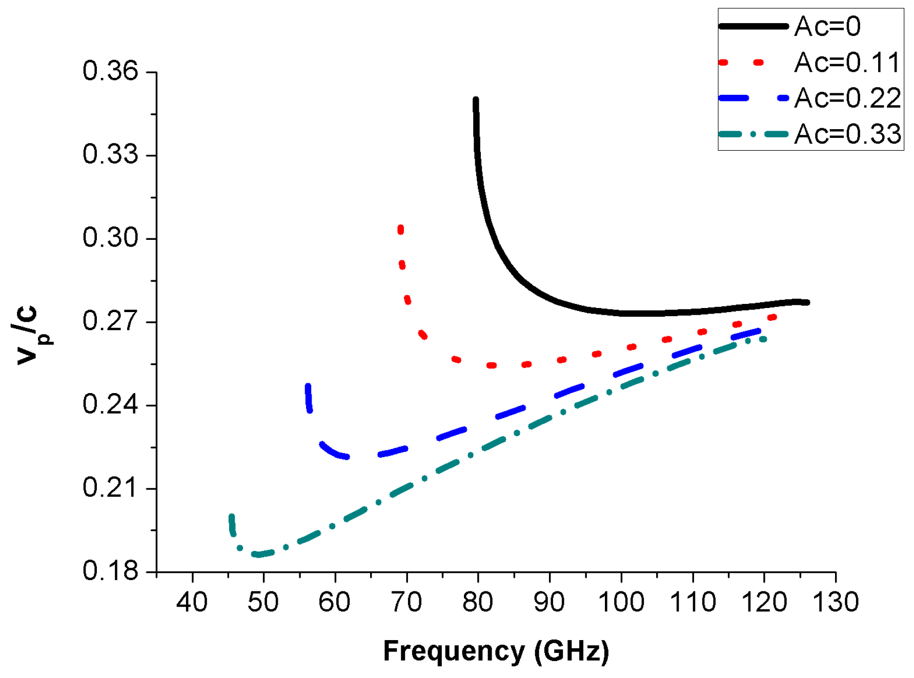
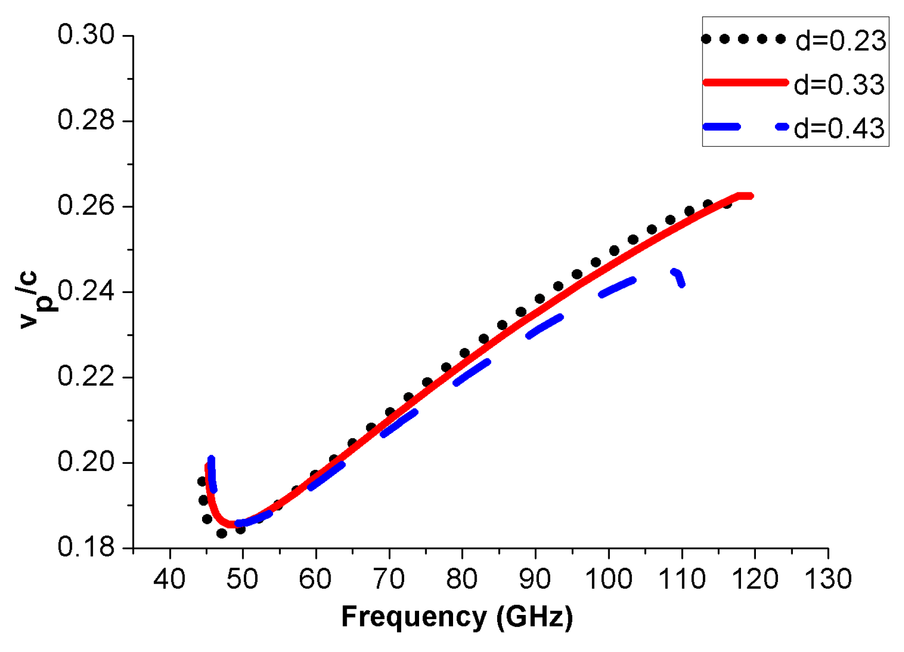
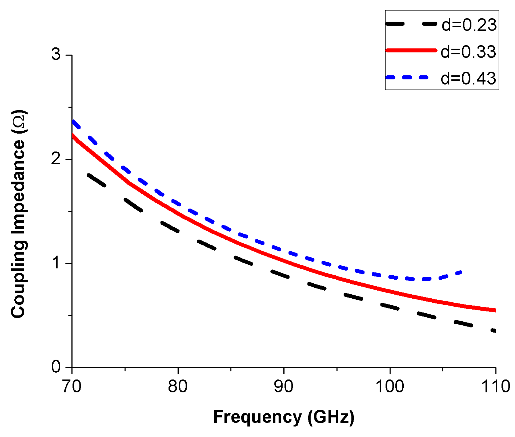
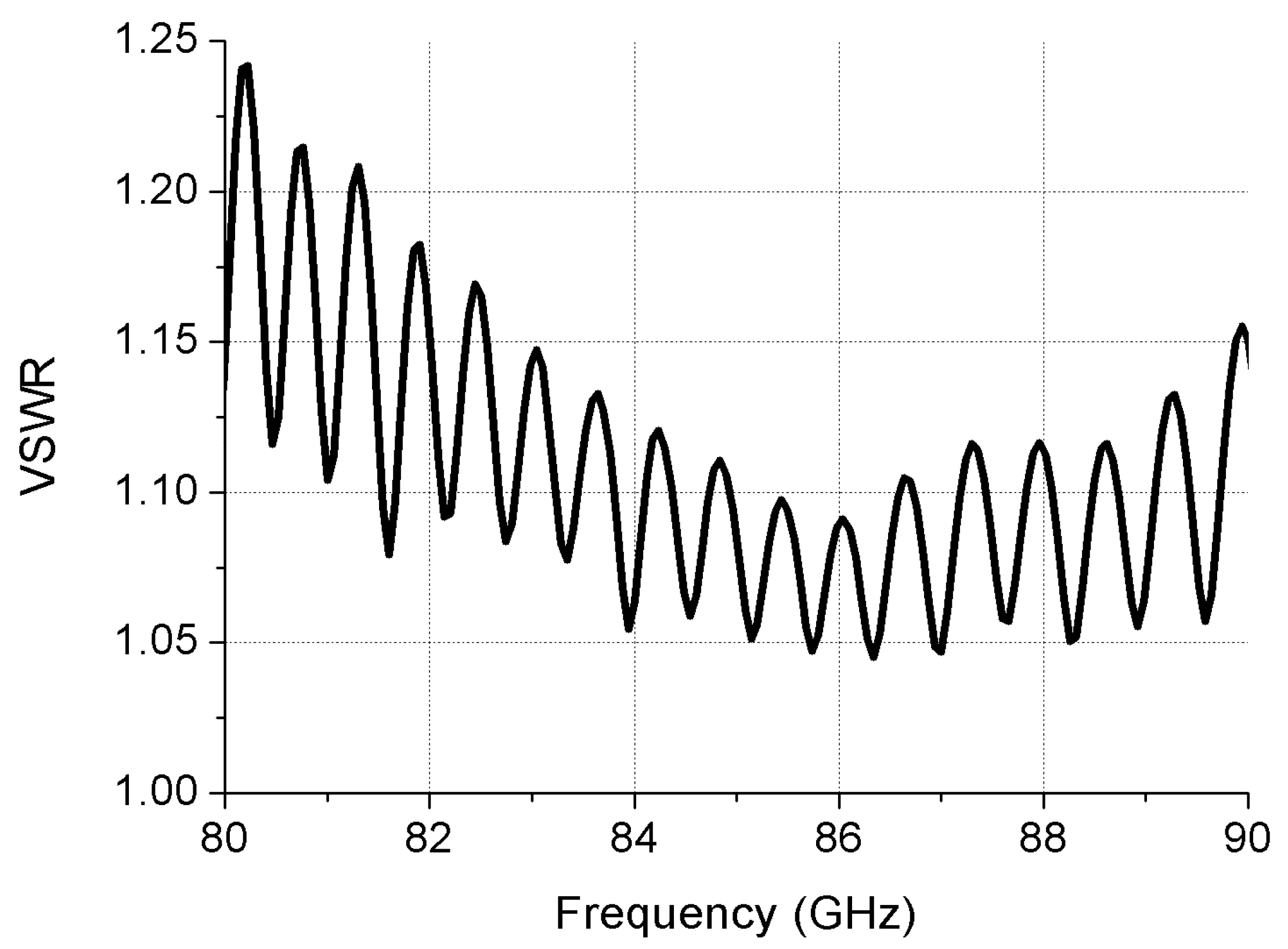
2. Analysis of Cold Characteristics
3. Design of Device
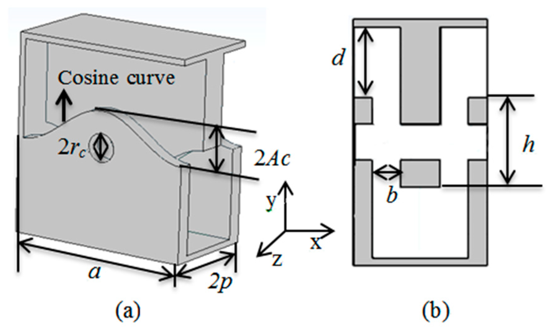
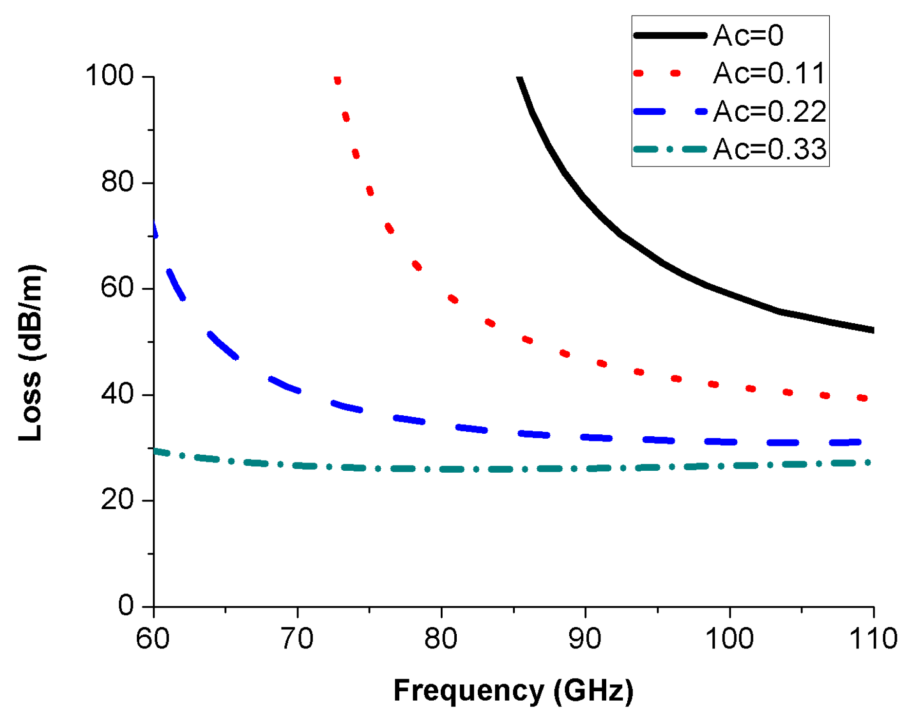
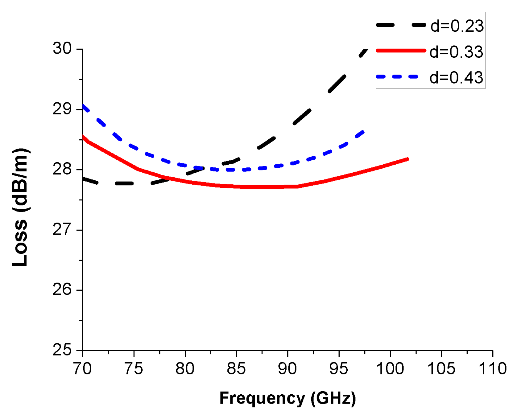
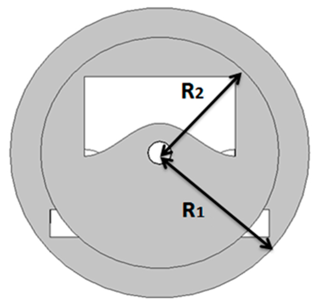
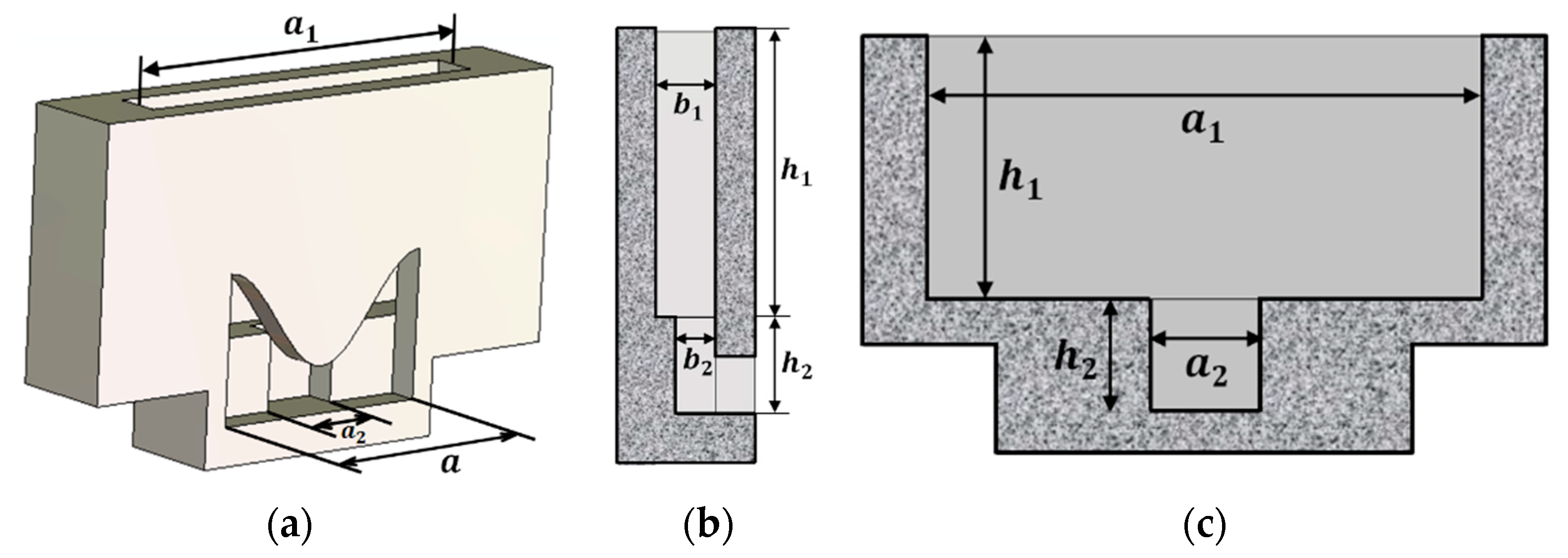
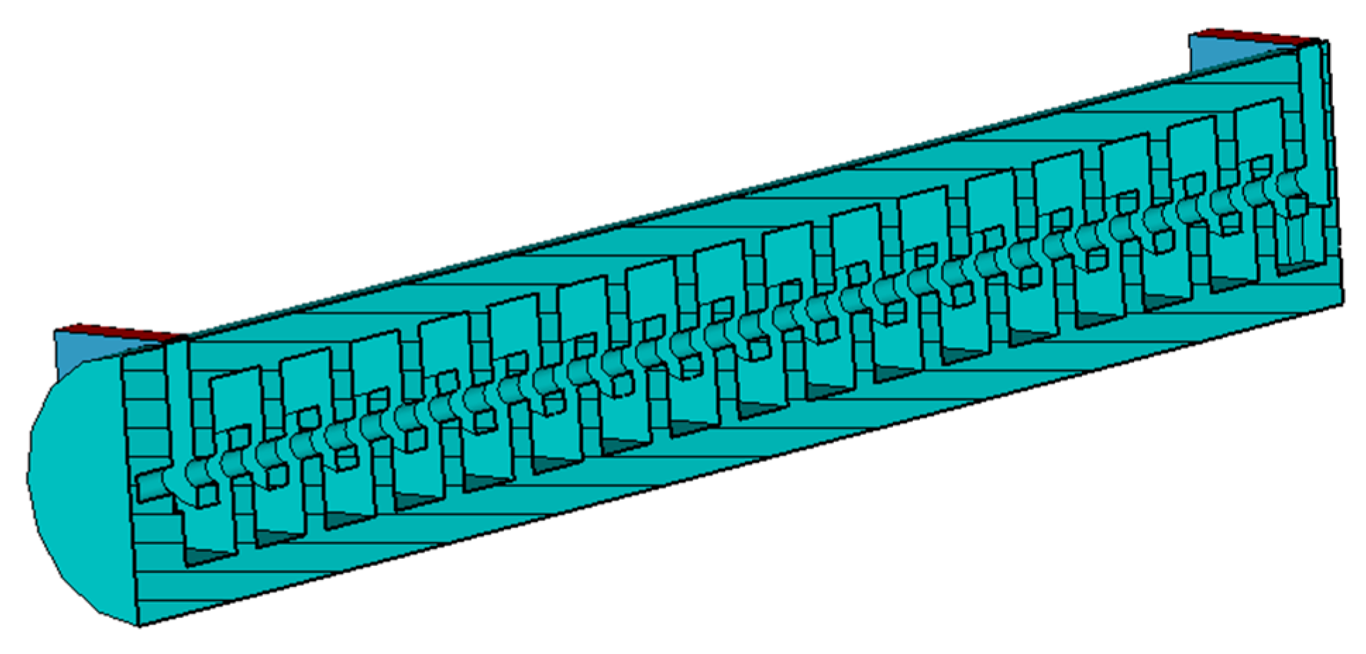
3.1. Design of SWS
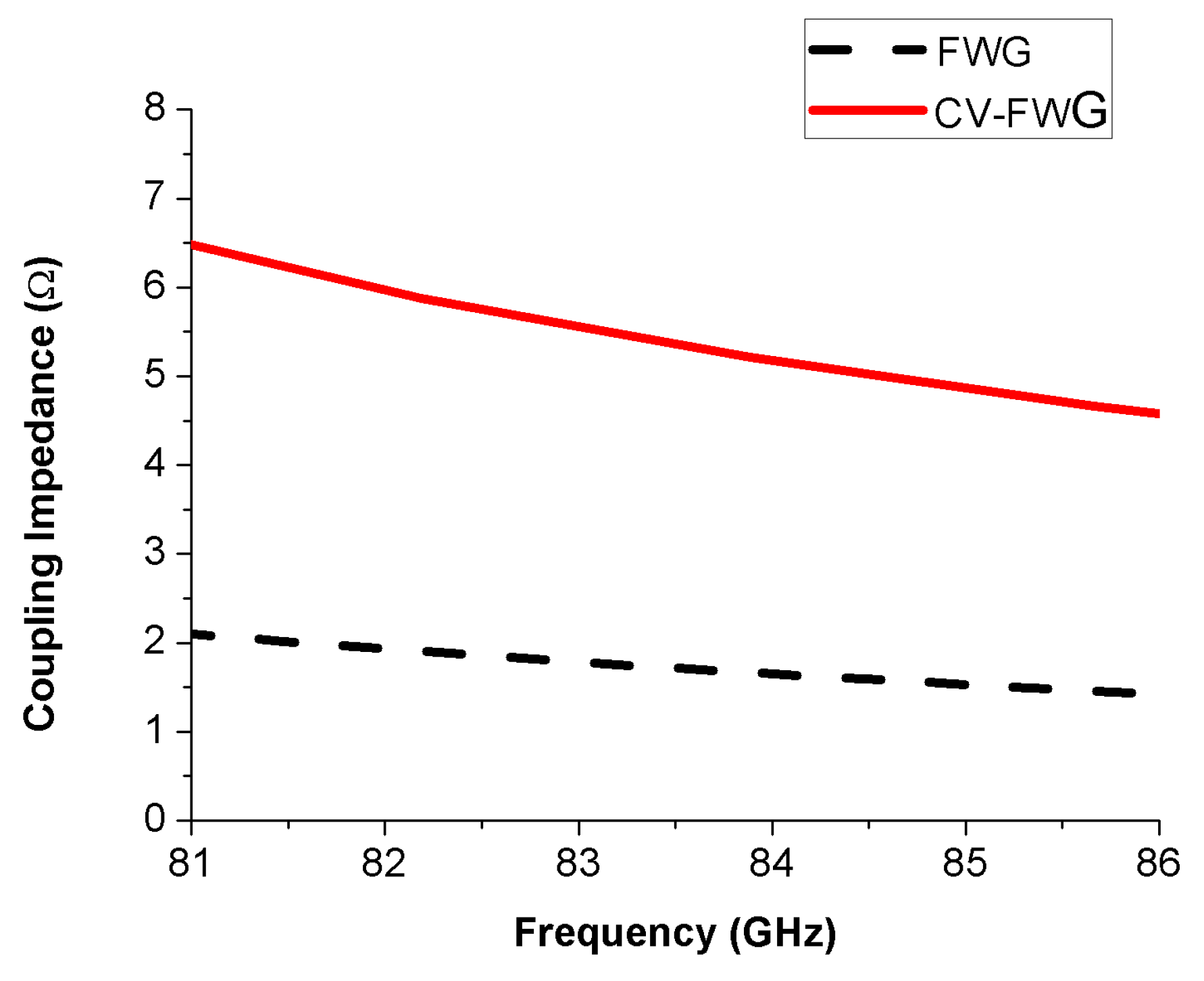
3.2. Miniaturized Coupler
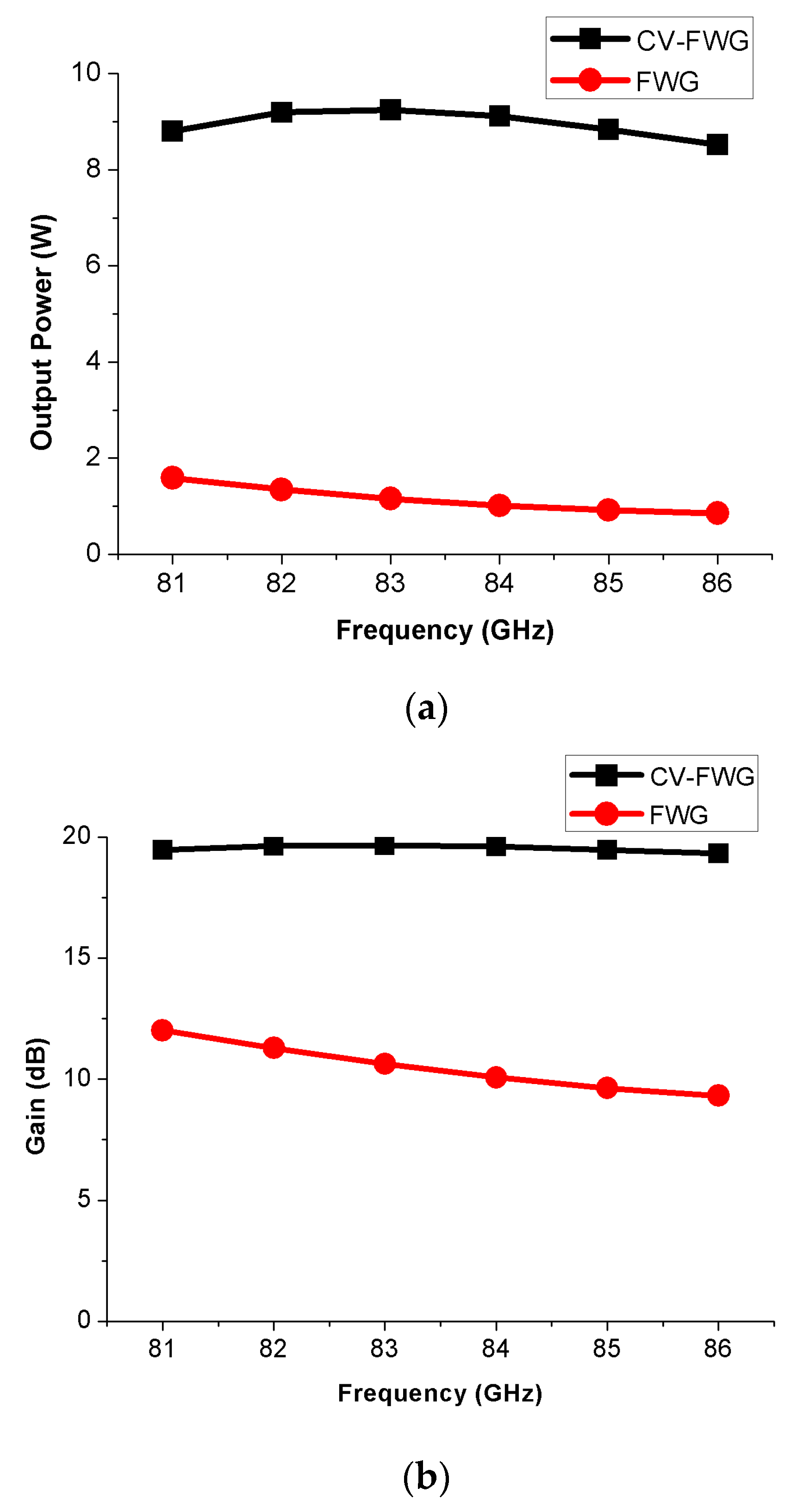
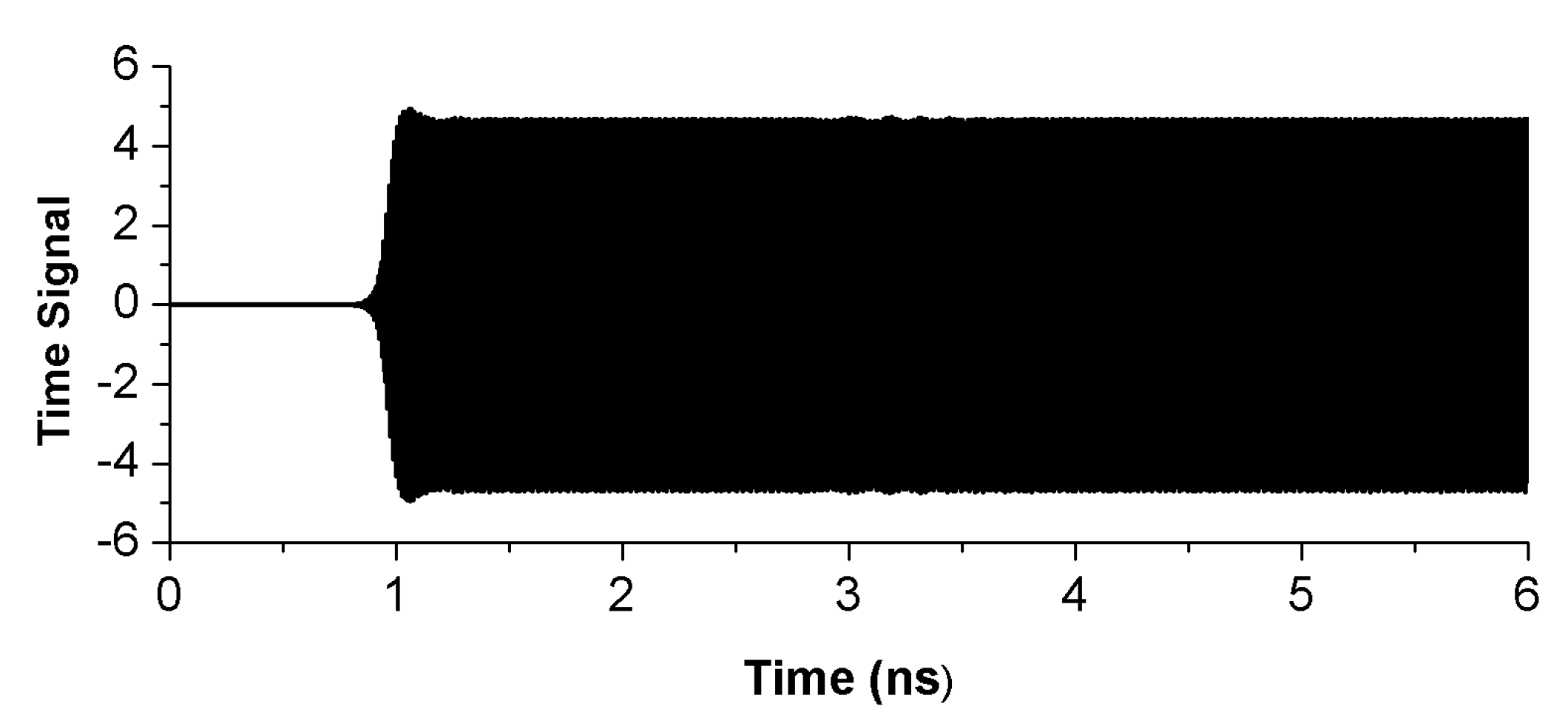
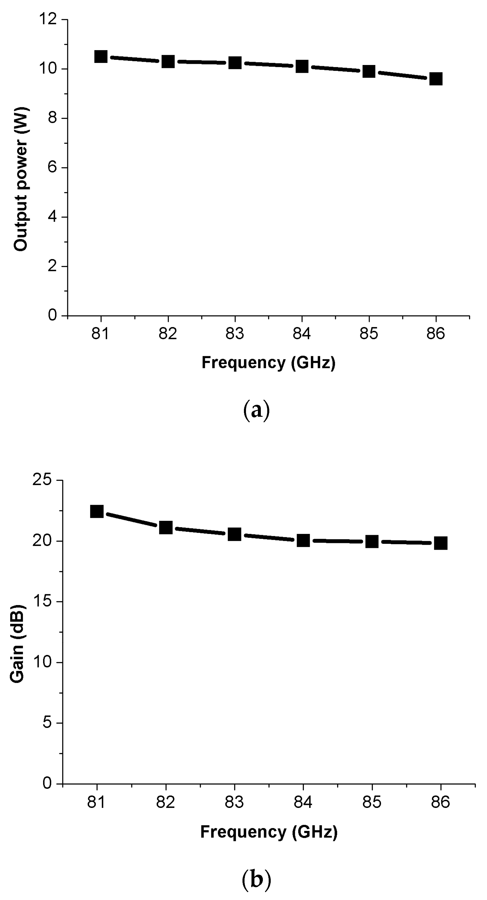
3.3. Beam–Wave Interaction
4. Conclusions
Author Contributions
Funding
Conflicts of Interest
References
- Federal Communication Commission: FCC 03-248. Allocation and Service Rules for the 71-76GHz, 81-86GHz, and 92-95GHz Bands; Federal Communications Commission: Washington, DC, USA, 2003. [Google Scholar]
- Lu, J.; Zhou, Z.; Wang, L.; Zeng, J.; Chen, S. Zero-multiplication TX-filter structure for E-band Transmission system. In Proceedings of the 2014 International Conference on Information and Communications Technologies, Nanjing, China, 16–18 May 2014; pp. 1–5. [Google Scholar]
- Ferndahl, M.; Gavell, M.; Abbasi, M.; Zirath, H. Highly integrated E-band direct conversion receiver. In Proceedings of the 2012 IEEE Compound Semiconductor Integrated Circuit Symposium, La Jolla, CA, USA, 14–17 October 2012; pp. 1–4. [Google Scholar]
- Ghassemi, N.; Wu, K. Planar High-Gain Dielectric-Loaded Antipodal Linearly Tapered Slot Antenna for E- and W-Band Gigabyte Point-to-Point Wireless Services. IEEE Trans. Antennas Propag. 2013, 61, 1747–1755. [Google Scholar] [CrossRef]
- Ghassemi, N.; Gauthier, J.; Wu, K. Low-Cost E-Band Receiver Front-End Development for Gigabyte Point-to-Point Wireless Communications. In Proceedings of the 43rd European Microwave Conference, Nuremberg, Germany, 6–10 October 2013; pp. 1011–1014. [Google Scholar]
- Pan, P.; Zi, Z.; Cai, J.; Tang, Y.; Liu, S.; Xie, Q.; Bian, X.; Feng, J. Millimeter Wave Traveling Tubes for High Data Rate Wireless Communication. Acta Electronica Sinica 2020, 48, 1834–1840. [Google Scholar]
- Li, Y.; Yue, L.; Qiu, B.; Gao, H.; Wang, S.; Zhao, G.; Xu, J.; Yin, H.; Duan, Z.; Huang, M.; et al. Design and Cold Test of a Ka-band Fan-Shaped Metal Loaded Helix Traveling Wave Tube. In Proceedings of the 2020 IEEE 21st International Conference on Vacuum Electronics (IVEC), Monterey, CA, USA, 19–22 October 2020; pp. 241–242. [Google Scholar]
- Liu, S.; Xie, Q.; Chen, Z.; Wu, Y.; Zi, Z.; Wu, X.; Cai, J.; Feng, J. High Linear Power E-Band Traveling-Wave Tube for Communication Applications. IEEE Trans. Electron Devices 2021, 68, 2984–2989. [Google Scholar] [CrossRef]
- Kowalczyk, D.; Zubyk, A.; Meadows, C.; Schoemehl, T.; True, T.; Martin, M.; Kirshner, M.; Armstrong, C. High Efficiency E-Band MPM for Communications Applications. In Proceedings of the IEEE 17th International Vacuum Electronics Conference (IVEC), Monterey, CA, USA, 19–21 April 2016; pp. 513–514. [Google Scholar]
- Zi, Z.; Liu, S.; Xie, Q.; Li, S.; Cai, J.; Zhao, S. A 70W 81-86GHz E-band CW Traveling Tube. In Proceedings of the IEEE International Vacuum Electronics, Busan, Korea, 28 April–1 May 2019; pp. 1–2. [Google Scholar]
- Ji, R.; Yang, Z.; Guo, Z.; Wang, Q.; Han, P.; Gong, H. Design and Experiment of An E-band Folded Waveguide Traveling Wave Tube. In Proceedings of the IEEE 20th International Vacuum Electronics Conference (IVEC), Busan, Korea, 28 April–1 May 2019; pp. 1–2. [Google Scholar]
- Kory, C.; Dayton, J.; Mearini, G.; Lueck, M. Microfabricated 94 GHz TWT. In Proceedings of the International Vacuum Electronics, Monterey, CA, USA, 17 July 2014; pp. 175–176. [Google Scholar]
- Dayton, J.; Kory, C.; Mearini, G. Microfabricated mm-wave TWT Platform for Wireless Backhaul. In Proceedings of the International Vacuum Electronics, Beijing, China, 27 August 2015; pp. 1–2. [Google Scholar]
- Cai, J.; Wu, X.; Feng, J. A Cosine-Shaped Vane-Folded Waveguide and Ridge Waveguide Coupler. IEEE Trans. Electron Devices 2016, 63, 2544–2549. [Google Scholar] [CrossRef]


| Frequency | 81–86 GHz |
|---|---|
| Beam voltage | Less than 10 kV |
| Beam current | Less than 20 mA |
| Peak output power | More than 8 W |
| RF input/output | WR-10 |
| Parameter | Dimensions (mm) | Reduction Percentage (%) | |
|---|---|---|---|
| CV-FWG | FWG | ||
| a | 1.6 | 2.4 | 33 |
| b | 0.2 | 0.3 | 33.33 |
| p | 0.45 | 0.55 | 18 |
| h | 0.6 | 1 | 40 |
| rc | 0.12 | 0.12 | 0 |
| Ac | 0.2 | - | - |
| d | 0.5 | - | - |
| R | 1.3 | 1.7 | 23.5 |
| S (mm2) | 5.3 | 9.1 | 41.8 |
Publisher’s Note: MDPI stays neutral with regard to jurisdictional claims in published maps and institutional affiliations. |
© 2021 by the authors. Licensee MDPI, Basel, Switzerland. This article is an open access article distributed under the terms and conditions of the Creative Commons Attribution (CC BY) license (https://creativecommons.org/licenses/by/4.0/).
Share and Cite
Ma, K.; Cai, J.; Feng, J. Investigation of a Miniaturized E-Band Cosine-Vane Folded Waveguide Traveling-Wave Tube for Wireless Communication. Electronics 2021, 10, 3054. https://doi.org/10.3390/electronics10243054
Ma K, Cai J, Feng J. Investigation of a Miniaturized E-Band Cosine-Vane Folded Waveguide Traveling-Wave Tube for Wireless Communication. Electronics. 2021; 10(24):3054. https://doi.org/10.3390/electronics10243054
Chicago/Turabian StyleMa, Kexin, Jun Cai, and Jinjun Feng. 2021. "Investigation of a Miniaturized E-Band Cosine-Vane Folded Waveguide Traveling-Wave Tube for Wireless Communication" Electronics 10, no. 24: 3054. https://doi.org/10.3390/electronics10243054
APA StyleMa, K., Cai, J., & Feng, J. (2021). Investigation of a Miniaturized E-Band Cosine-Vane Folded Waveguide Traveling-Wave Tube for Wireless Communication. Electronics, 10(24), 3054. https://doi.org/10.3390/electronics10243054