Abstract
We describe two models of Power Transistors (IGBT, MOSFET); both were successfully used for the analysis of electromagnetic interference (EMI) and electromagnetic compatibility (EMC) while modeling high-voltage systems (PFC, DC/DC, inverter, etc.). The first semi-mathematical–behavioral insulated-gate bipolar transistor (IGBT) model introduces nonlinear negative feedback generated in the semiconductor’s p+ and n+ layers, which are located near the metal contact of the IGBT emitter, to better describe the dynamic characteristics of the transistor. A simplified model of the metal–oxide-semiconductor field-effect transistor (MOSFET) in the IGBT is used to simplify this IGBT model. The second simpler behavioral model could be used to model both IGBTs and MOSFETs. Model parameters are obtained from datasheets and then adjusted using results from a single measurement test. Modeling results are compared with measured turn-on and turn-off waveforms for different types of IGBTs. To check the validation of the models, a brushless DC electric motor test setup with an inverter was created. Despite the simplicity of the presented models, a comparison of model predictions with hardware measurements revealed that the model accurately forecasted switch transients and aided EMI–EMC investigations.
1. Introduction
Power transistors are the main source of electromagnetic interference (EMI) and electromagnetic compatibility (EMC) problems in power devices. In the modern metal–oxide-semiconductor field-effect transistor (MOSFET) and insulated-gate bipolar transistor (IGBT), switching times range from 30 to 200 ns, and switching currents may exceed 2000 A with high voltage (>4500 V). To simulate power devices from an EMI–EMC standpoint, focus should be on the noise generation mechanisms inside transistors.
Much research has been devoted to power transistor modeling. For example, “A Review of IGBT Models” [] reviews transistor models in the literature before the year 2000, analyzing, comparing, and classifying them by type of mathematics, objectives, complexity, accuracy, and speed. We focus on IGBT models consisting of MOSFET and PNP transistors. Physics-based analytical models are represented in articles by A.R. Hefner [,,,], D.S. Kuo [,], R.J. McDonald [] (whose works provided the fundamentals for the IGBT basic model in Simulation Program with Integrated Circuit Emphasis (SPICE) simulators), B.J. Baliga [], G.M. Strollo [], F. Mihalic [], Han-Soo Kim [], Ying-Yu Tzou [], Z. Shen [], J.T. Hsu [], S. Musumeci [], J.L. Tichenor [], A. Tone [], and Jinlei Meng []. In reviewing the models, we found that those based on the ambipolar diffusion equation [,,,,,,,,] are characterized by high accuracy and that convergence problems are seldom revealed after model refinement. Parameters required to build a model are difficult to obtain [,,], and even if all parameters are present, substantial time and qualified personnel are required to assemble the model.
Factory SPICE models are mainly based on the above method. However, due to their complex modeling systems, when several models of transistors are required simultaneously, the modeling time increases when factory models are used, which can lead to frequent convergence problems [,]. In reviewing the simpler models, which mainly use the behavioral modeling principle based on semiconductor devices physics [,,,,,,,,], we found that the most of these models are optimized for certain situations. It remains unclear how to get these models and optimize their parameters.
In this paper, we present a methodology for the generation and usage of EMI–EMC applications in two variants of power transistor models optimized for simulations of power devices:
- (1)
- A model accurately describing the operation of an IGBT that is as simple and universal as possible; and
- (2)
- A simple model illustrating only the basic parameters of transistors but capable of modeling EMC–EMI problems.
An important requirement is that the models do not create or complicate convergence problems during calculations. The first model is a combination of semi-mathematical and behavioral models based on the physics of semiconductor devices. While working on the model, we observed that impedance of the p+ and n+ layers located near the emitter influenced the transistor parameters. A novelty of this model is the addition of nonlinear, current-dependent resistance near the emitter, which increases the accuracy of the model in static and dynamic modes. The creation of this model requires complicated procedures. The first model is useful for capturing the fine effects caused by the interaction of the transistor’s nonlinear parasitic capacities with the outer circle.
The second model is a behavioral model requiring only seven parameters for proper operation. These parameters are obtained from the transistor datasheet. As practical experience has shown, the second model is sufficient in most EMI/EMC applications and gives good results.
The rest of the paper is structured as follows. The methodology underlying the first complex modeling of an IGBT is presented in Section 2. Section 3 describes the measurement procedure required for model validation. Section 4 discusses the creation of simple IGBT and MOSFET models. Section 5 reviews the calculations times. In Section 6, we present an experimental setup of a brushless DC motor with an inverter and modeling of this setup. Section 7 concludes.
2. Methodology
Our methodology consists of the following steps:
- Construction of a simulation model for an IGBT for SPICE using the initial parameter values obtained from datasheets;
- Construction of a test bench for the IGBT;
- Measurements of input and output voltages;
- Construction of a simulation model of the test bench;
- Simulation of input and output voltages and adjustment of the IGBT parameters to fit the measurement results;
- Testing of the IGBT models for different levels of controlling signals;
- Testing of the IGBT models in the presence of different loads.
2.1. Equivalent Circuit Model of an IGBT
General circuit models of IGBTs consist of a combination of MOS and PNP bipolar junction transistors (Figure 1a). The nonlinear input capacity and feedback capacity of the MOSFET are modeled with three capacitors, C1, C2, and C3 (Figure 1b).
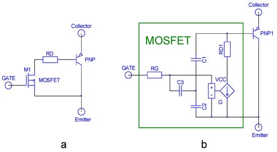
Figure 1.
General circuit models of the IGBT showing the (a) MOS (metal–oxide-semiconductor) and PNP bipolar junction transistor and (b) three capacitors, C1, C2, and C3.
In the first model, we used three diodes (D1, D2, and D3) to describe them (Figure 2). For the MOS transistor M1, which is included in the IGBT (Figure 1) circuit, we replaced the voltage-controlled current source G1 (Figure 2). The formulas used in our model accurately describe the law of change in the capacity of the p–n junction, according to the voltage across the p–n junction.
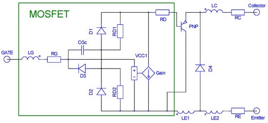
Figure 2.
Equivalent circuit model of the IGBT (Insulated Gate Bipolar Transistor).
Diodes D1 and D2 describe the current change directly in the p–n junctions, and diode D3 describes the change in capacitance caused by a change in the excitation of the adjacent semiconductor layers of the gate. Since the gate is placed in a SiO2 (dielectric) environment, its magnitude should not change. However, as shown in Figure 3, where the topological structure of the IGBT transistor is given, the total gate capacitance consists of a constant component (gate capacitance to the emitter metal CGc Figure 2) and a variable part (D3 describes this capacitance) that is created when the gate interacts with a semiconductor structure (n+, p−, n−, p−, n+). The conductivity of these layers varies from almost fully insulated to fully conductive.
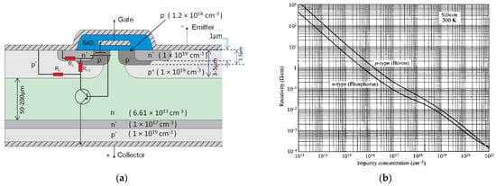
Figure 3.
Diagram of IGBT cell (a) and resistivity vs. impurity concentration at 300 K for silicon (b) from [].
It is likely that the law of change of such additional capacity differs from the law of change of the capacity of the diode, although our results show that such an assumption gives a fairly accurate result. Note that in all variants of SPICE, the diode is described in the same way. Thus, if we enter IBV = 0, IBVL = 0, IS = 0, and ISR = 0 in the model, the power goes out and only capacity works, according to the PSpice reference guide [].
Here, Vj is the threshold potential; V is the voltage across the p–n junction; and Cj0 is the threshold capacity when V = 0. M and Fc define the nonlinearity parameters.
Diodes D3 and D2 are respectively connected in parallel with resistors RD3 and RD2. These resistors create an additional initial constant bias voltage, which is necessary for the correct starting values of the diode capacities and to maintain a non-zero value of the current in the external circuit to improve convergence. The values of these resistors should be selected so that they do not affect the basic parameters of the transistor. The gain coefficients of voltage-controlled voltage sources are calculated as follows:
where is the driving voltage, is the threshold voltage, and α, β, and γ are coefficients. LG and RG indicate the connecting wire inductance and total resistance of the gate, respectively. Parasitic inductances and resistances of the emitter and collector are modeled by LE1, LE2, Lc, and RE. The p–n–p transistor model is taken from the SPICE standard table (MODEL QSUB PNP).
Our investigations demonstrated that the equivalent scheme presented in Figure 2 describes the cut-off and saturation states of the IGBT but is not accurate enough to describe the active linear states (see Section 3 for a detailed discussion on this issue). In our opinion, the reason for this is the nonlinear negative feedback generated by the volumetric resistances in the n+, p+, and n− layers near the emitter contact (Figure 3a).
The magnitudes of resistors Rs, Rc, and Rcs (Figure 3a and Figure 4a) depend on the emitter current. As shown in Figure 4, they form a negative feedback loop. The value of these resistors can range from 0.01 to 1 Ohm when the transistor is locked (i.e., VG ≤ Vtr) and within 0.1 and 10 mOhms when the transistor is in active mode (i.e., VG ≥ Vtr) [,,]. This is due to the high doping level of the emitter’s n+ and p+ layers (Figure 3b) and therefore their low impedance of 1–10 mOhm/sm [].
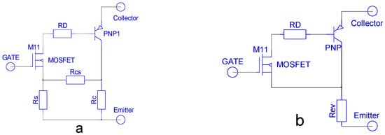
Figure 4.
Updated general circuit of the IGBT negative feedback resistor connection schematic in the IGBT (a,b) simple versions of this connection.
Since they vary by one law according to the current (i.e., a good approximation can be described for a single resistor), it is possible to replace them with an equivalent single resistor (Figure 4b).
We can model this nonlinear impedance using a voltage-controlled current source Gr, as in Figure 5, with a transmission coefficient Gr as follows:
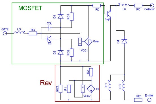
Figure 5.
Equivalent circuit model of the IGBT.
The concentration of current carriers (electrons and holes) and current increase exponentially; hence, the volumetric impedance of the layers of the semiconductor structure of the transistor decreases by the same exponential law. The law of change of the Rev resistor (Figure 4b) also is exponential, as shown in Equation (3). RE2 determines the initial value of the nonlinear impedance; R1 and R2 comprise the current sensors (Figure 5).
Their values are specified in the modeling process by correlating them with the measurement results. The initial value can be selected according to the concentration of dopants in the IGBT emitter layers [,,]. Their values range from R1 = 0.1–1 mΩ, R2 = 0.1–1 mΩ, and RE2 = 0.1–1 Ω. The new scheme in Figure 5 is more accurate than the one represented in Figure 2, as shown in Figures 10–12 in Section 3.
2.2. Procedure to Generate Parameters of the Equivalent Circuit Model of the IGBT
Our procedure for adjusting the parameter values is based on measurements. Test bench (Figure 6) and measurement procedure of IGBT characteristics is applicable to all transistor modules tested. The schematic of the test printed circuit board shown on Figure 7a. However, the design of each printed circuit board (Figure 7b and Figure 11) depends on the transistor packaging and configuration of power and control terminals. The PCB layout is designed to reduce its influence on measured quantities as much as possible. The two-layer PCB bottom is completely grounded. Copper bus bars in the bottom and top layers reduce ground resistance, which in turn reduces the voltage drop across the ground electrode and improves the measurement results.
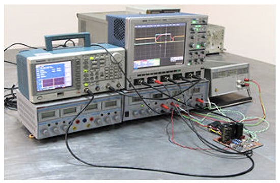
Figure 6.
Measurement test-bench setup.
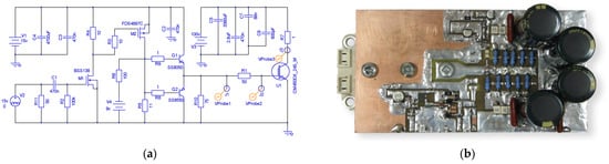
Figure 7.
(a) Schematic of PCB for measuring IGBT characteristics, (b) test-bench PCB designed for SEMIKRON module SKM200GB123D.
Using a test bench (Figure 6), we measured voltage waveforms using an oscilloscope (Lecroy WaveRunner 04Xi 2 Ghz 10 GS/s) at the collector (Figure 7a, Probe 3) and at the gate (Figure 7a, Probe 2) of the IGBT for different levels of pulse input voltage (Figure 7a, Probe 1). Parameter adjustment was considered complete when the equivalent circuit could describe the behavior of the IGBT module with minimum errors in all working modes that were measured.
To generate the required input voltage, we used a pulse amplifier based on M1, M2, Q1, and Q2 transistors (Figure 7a). The pulse voltage at the output of the amplifier was regulated by the voltage of the DC source V1. Elements R11, C1, and R2 matched the high-resistance input of the M1 (BSS138) transistor, with 50 Ohm input impedance of the signal generator V2 (Tektronix AFG3252 240 Mhz 2 GS/s). Transistor M2 (FDS4897C) had low drain-source impedance (RDS(on) = 63 mΩ), which reduced the influence of the input port on the charging and discharging processes of the input capacitances in transistors Q1 (SS8050) and Q2 (SS8550). These transistors formed the output stage of the amplifier and had minimal output impedance and thus minimal influence on the measured quantities. In this case, the charging and discharging processes of the input capacitance of transistor U1 depended completely on resistor R1. Thus, we used high-resistance probes connected to resistor R1 (see Figure 7a).
The IGBT under investigation had an R7 load on the collector, which comprised 18 Ω 2W low-inductive resistors connected in parallel. To decouple the power supply line from the test-bench PCB, several capacitors (C2–C8) of different types were used. Section 3 describes the test-bench examples and results.
3. Model Verification
Several transistors of different types were examined. In this section, we present the results for the two IGBT modules.
3.1. Modeling of SEMIKRON Module SKM200GB123D
IGBT module SKM200GB123D is from SEMIKRON and based on a non-punch-through-type IGBT with an integrated diode. Using this transistor model, we present a comparison of the basic (Figure 8a) and improved (Figure 8b) models in Figure 8.
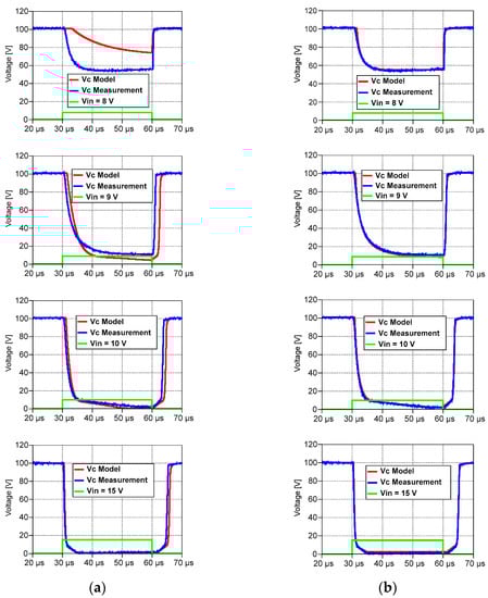
An advantage of the improved model is that it is more accurate when the input voltage level is close to the threshold voltage. Figure 9 shows the collector voltage fall and Rise diagram when the pulse voltage at the gate is 15 v.
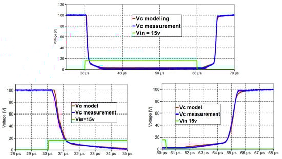
Figure 9.
Collector voltage for 15 V input pulse.
Figure 10 represents the modeled and the measured voltages at gate for 15 V of input. The graphs in Figure 8, Figure 9 and Figure 10 are for R1 = 50 Ohm (Figure 7a). When the value of R1 decreases, the switching time decreases to the minimum time of the transistor being tested.
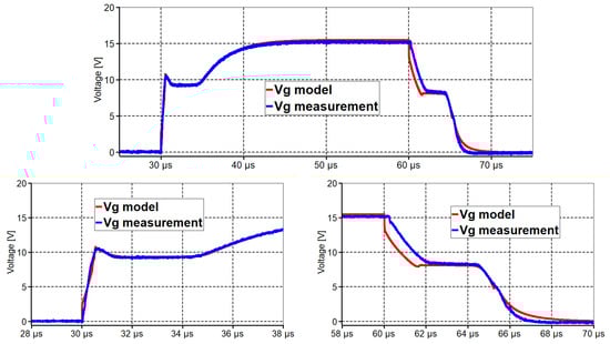
Figure 10.
Gate voltage for 15 V input pulse.
3.2. Modeling of Mitsubishi Electric Model CM450DX-24S
Figure 11 shows the test-bench PCB (Printed Circuit Board) designed for Mitsubishi Electric IGBT, Model CM450DX-24S.
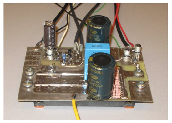
Figure 11.
Test-bench PCB with attachment for Mitsubishi Electric CM450DX-24S module.
Figure 12 and Figure 13 represent the results for 15 V of input. Once again, the new model demonstrated high accuracy in comparison with measurements.
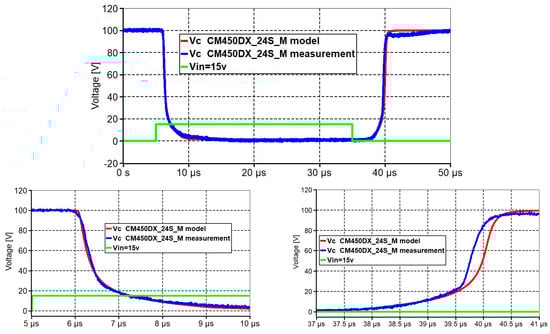
Figure 12.
Simulated and measured collector voltages for the Mitsubishi Electric CM450DX-24S module.
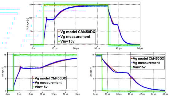
Figure 13.
Simulated and measured gate voltages for the Mitsubishi Electric CM450DX-24S module.
Figure 9, Figure 10, Figure 12, and Figure 13 present the good matching of measurement and modeling results. Figure 9 (SKM200GB123D) and Figure 12 (CM450DX-24S) show the change in collector voltage of the IGBT transistor when a 15 V amplitude pulse signal is supplied to the GATE; as it can be seen from the figure, the shapes of the Fall and Rise signals are almost identical in the measured and modeled graphs. The IGBT transistor is supplied with a signal at GATE through 50 Ohm resistors. This allowed us to better understand the current processes at the GATE, which are the complex result of the process of charging and discharging the parasitic capacities of the transistor. Figure 10 (SKM200GB123D) and Figure 13 (CM450DX-24S) show the voltage change pattern on the GATE in the event of 50 Ohms. Here, it should be noted that the signal forms match each other quite well. Small time differences do not have a significant impact on the device modeling results.
4. EMC-Oriented Model of IGBTS and MOSFETS
In this section, we describe an even simpler model of power transistors that can be used to model both IGBTs and MOSFETs. This simple model requires a much smaller number of parameters than the improved model we described above (Figure 5). Thus, it is recommended for preliminary analysis of electronic systems because it reduces design time and computing resources by accelerating calculations by up to 10 times. The parameters used in the model are as follows:
Ron: drain-source on-state resistance;
Roff: drain-source off-state resistance;
Vdr: input drawing pulse signal amplitude;
Vtr: gate threshold voltage;
Ciss: input capacitance;
Coss: output capacitance;
Crss: reverse capacitance.
All these parameters can be found in the transistor datasheet. For example, Figure 14 shows the transistor diagram and SUBCKT file. We conventionally call it RMOS0101D.
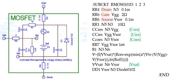
Figure 14.
The transistor diagram and SUBCKT file.
Resistance is changed by exponential law:
where a = 2 × (ln(Ron/Roff))/(Vtr − Vdr). The minimum and maximum values of resistance, Ron and Roff, respectively, are bounded (limited) by the “min” function. The rate of change of R from Ron to Roff depends on coefficient “a.” In general, the selection of the value of “a” should be done with the help of an optimization program. (The given formula is its empirically selected best option.) In Figure 15, the simulation design for RMOS0101D is represented with resistive and inductance loads. Figure 16 and Figure 17 show the results of the modeling.
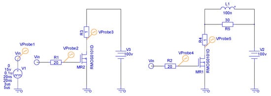
Figure 15.
Simulation design for RMOS0101D with resistive and inductance loads.
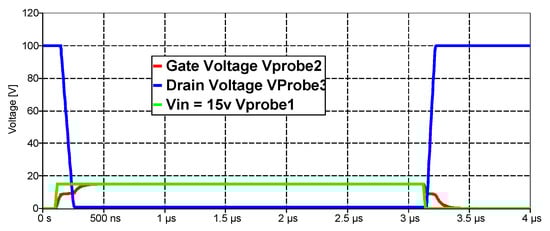
Figure 16.
RMOS0101D with resistive load (Figure 15).
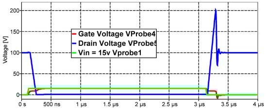
Figure 17.
RMOS0101D with inductive-resistive load (Figure 15).
We compared the accuracy model (Figure 5) for the Mitsubishi Electric CM450DX-24S1 module and the simple model for transistor RMOSCM450DM (Figure 18 and Figure 19) with measurement data. Figure 18 shows the transistor diagram and SUBCKT file.
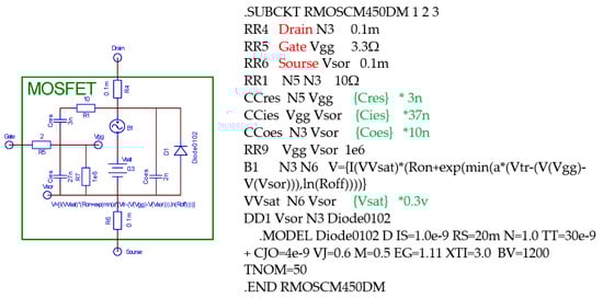
Figure 18.
Model of CM450DX-24S1.
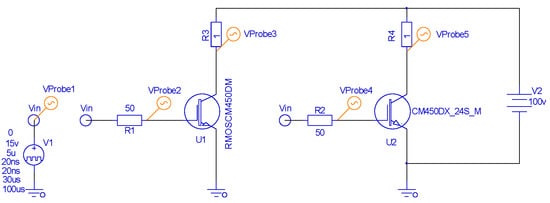
Figure 19.
CM450DX-24S modeling test schematic.
This model uses the same exponential function of impedance change as in the previous simple model.
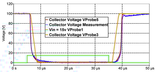
Figure 20.
Collector and gate voltages with R1 = R2 = 50 Ohm (Figure 19).
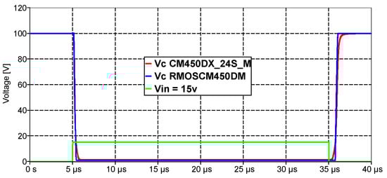
Figure 21.
Rise and Fall time with R1 = R2 = 1 Ohm (Figure 19).
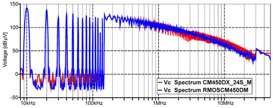
Figure 22.
Collector voltages spectrum with R4 = R3 = 1 (Figure 19).
If for solving the problem, we need an accurate description of the transient characteristics of the transistor, a simple model is insufficient for this level of simulation (Figure 20). As shown in Figure 21, if only the fast-switching mode of the transistor is needed, then to determine how the currents generated in the circuit are distributed and quickly detect unwanted resonances of filters and wires (EMC problems), a simple model offers a stable and fast solution. Figure 21 shows that the fall and release times, which determine the amplitude and bandwidth of the spectrum, are fairly well described (Figure 22).
We tested the transistors by modeling different types of circuits, such as an inverter, DC–DC converter, power factor corrector, charger, filter, and joint operation. Along with the cables of the listed devices, the modeling was successful. In all cases, the calculations were stable. The signals obtained during modeling and the shape of their spectra matched the measurement results (Figures 26 and 27). The accuracy also was sufficient to detect parasitic resonances in complex harnesses and to determine the causes of their occurrence. The acceleration of the calculation allows engineers to conduct more modeling experiments and solve the problem in a short time.
5. Calculation Times
To compare the calculation times for different transistor models, we used a relatively simple inverter model using space vector pulse width modulation with a filter and a simple motor (Figure 23).
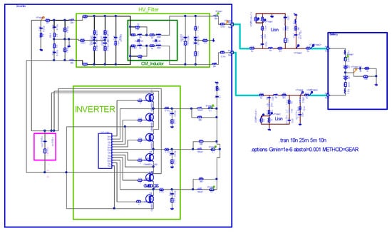
Figure 23.
Simple inverter setup.
The results of the calculation times are shown in Table 1.

Table 1.
Results of calculation time.
6. EMC-Oriented Model of IGBT and MOSFET
We assembled an operating stand for the UQM Powerphase 100 (Figure 24).
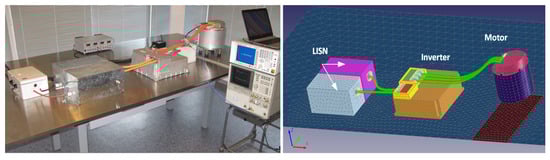
Figure 24.
Photo and 3D model of UQM Powerphase 100 setup.
A complete model of this stand was created, including the inverter with space vector pulse width modulation, DC link capacitor, high-voltage filter, line impedance stabilization networks, simplified battery model, and motor and cable models. Modeling was performed in stages. First, we measured the S parameters of the filter and then determined the internal structure of the CM coil using X-ray computed tomography. Based on this information, we created a CM inductance model. Then, the complete filter model was created. Using the same method, the DC link capacitor and motor models were developed, along with an inverter model with SVPWM modulation. The modeling was done using EMCoS Studio, which allowed the creation of high-voltage cable models to assemble and calculate the complete power train system model. Figure 25 shows the full model of the stand.
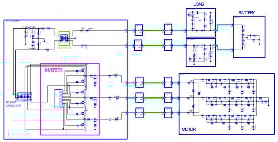
Figure 25.
UQM Powerphase 100 setup model.
The model is large and requires optimized transistor models. Thus, we used both a complex IGBT model (CM450DX; Figure 5) and a simple model (RMOS450DX; Figure 21), the parameters of which we took directly from the transistor datasheet.
Figure 26 and Figure 27 show the modeling results. The simple transistor model did not differ much in the calculations, compared to the complex model. Therefore, we concluded that during the EMC pre-analysis of complex systems (e.g., the electrical wiring of a car, ship, aircraft, or other equipment), when it is necessary to detect and prevent parasitic resonances, it is sufficient to use the proposed simple model to save time.
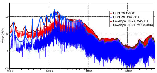
Figure 26.
Modeling comparison for CM450DX and RMOS450DX models showing spectra of the LISN.
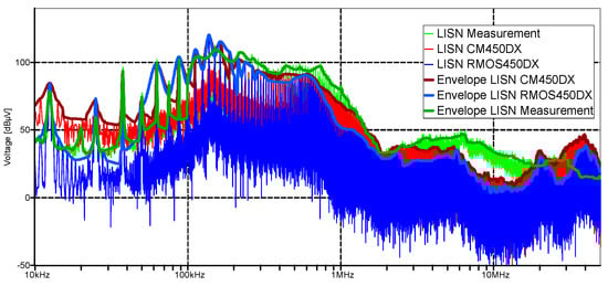
Figure 27.
Measurement and modeling comparison.
7. Conclusions
In our paper, we present IGBT modeling that describes transistor characteristics for use in both EMI–EMC and circuit analyses. Two transistor models were developed, both of which account for the physical processes in the semiconductor layers and near the emitter. We introduced nonlinear feedback into the overall circuit model of the IGBT, which significantly improved the simulation of the dynamic characteristics of IGBTs. Moreover, the developed model is relatively simple and robust, which provides advantages in EMI–EMC simulations of complex power devices.
The parameter extraction methodology is based on the values obtained from the IGBT datasheet. Further adjustments were made by comparing simulations and measurements using a single test panel. The second model is an approximate model of the transistor, which can be used only to analyze pulse switching circuits. Nevertheless, it has the advantage of simplicity of setup and stable operation, and it can be used to replace both IGBTs and MOSFETs. Test set modeling with a brushless DC electric motor and inverter demonstrated the applicability of the developed models.
Author Contributions
Conceptualization, B.K.; methodology, B.K.; software, A.G. and R.J.; validation, B.K., Z.K. and A.G.; formal analysis, B.K., A.G., Z.K. and R.J.; investigation, B.K., A.G. and Z.K. All authors have read and agreed to the published version of the manuscript.
Funding
EM Consulting and Software, EMCoS.
Informed Consent Statement
Informed consent was obtained from all subjects involved in the study.
Data Availability Statement
All data included in this study are available upon request by contacting with the corresponding author.
Acknowledgments
The authors would like to thank David Pommerenke and Michael Fuchs for supportive discussions, recommendations, and encouragement.
Conflicts of Interest
The authors declare no conflict of interest.
References
- Sheng, K.; Williams, B.; Finney, S. A review of IGBT models. IEEE Trans. Power Electron. 2000, 15, 1250–1266. [Google Scholar] [CrossRef]
- Hefner, A.R. Analytical modeling of device-circuit interactions for the power insulated gate bipolar transistor (IGBT). IEEE Trans. Ind. Appl. 1988, 1, 606–614. [Google Scholar] [CrossRef] [Green Version]
- Hefner, A.R. Modeling buffer layer IGBTs for circuit simulation. IEEE Trans. Power Electron. 1995, 10, 111–123. [Google Scholar] [CrossRef]
- Mitter, C.S.; Hefner, A.R.; Chen, D.Y.; Lee, F.C. Insulated gate bipolar transistor (IGBT) modeling using IG-SPICE. IEEE Trans. Ind. Appl. 1994, 30, 24–33. [Google Scholar] [CrossRef]
- Hefner, A.; Bouche, S. Automated parameter extraction software for advanced IGBT modeling. In Proceedings of the COMPEL 2000 7th Workshop on Computers in Power Electronics (Cat. No.00TH8535), Blacksburg, VA, USA, 16–18 July 2000; pp. 10–18. [Google Scholar] [CrossRef]
- Kuo, D.-S.; Choi, J.-Y.; Giandomenico, D.; Hu, C.; Sapp, S.; Sassaman, K.; Bregar, R. Modeling the turn-off characteristics of the bipolar-MOS transistor. IEEE Electron. Device Lett. 1985, 6, 211–214. [Google Scholar] [CrossRef]
- Kuo, D.-S.; Hu, C.; Sapp, S.P. An analytical model for the power bipolar-MOS transistor. Solid-State Electron. 1986, 29, 1229–1237. [Google Scholar] [CrossRef]
- McDonald, R.J.; Fossum, J.G. High-voltage device modeling for SPICE simulation of HVICs. IEEE Trans. Comput.-Aided Des. Integr. Circuits Syst. 1988, 7, 425–432. [Google Scholar] [CrossRef]
- Baliga, B.J. Analytical modeling of IGBTs: Challenges and solutions. IEEE Trans. Electron Devices 2013, 60, 535–543. [Google Scholar] [CrossRef]
- Strollo, A.G.M. A new IGBT circuit model for SPICE simulation. In Proceedings of the PESC97, Record 28th Annual IEEE Power Electronics Specialists Conference. Formerly Power Conditioning Specialists Conference 1970–71, Power Processing and Electronic Specialists Conference 1972, St. Louis, MO, USA, 27 June 1997; Volume 1, pp. 133–138. [Google Scholar] [CrossRef]
- Mihalic, F.; Jezernik, K.; Krischan, K.; Rentmeister, M. IGBT SPICE macro model. In Proceedings of the 1992 International Conference on Industrial Electronics, Control, Instrumentation, and Automation, San Diego, CA, USA, 13 November 1992; Volume 1, pp. 240–245. [Google Scholar]
- Kim, H.; Cho, Y.; Kim, S.-D.; Choi, Y.-I. Parameter extraction for the static and dynamic model of IGBT. In Proceedings of the IEEE Power Electronics Specialist Conference, Seattle, WA, USA, 20–24 June 1993; pp. 71–74. [Google Scholar] [CrossRef]
- Tzou, Y.-Y.; Hsu, L.-J. A practical SPICE macro model for the IGBT. In Proceedings of the IECON ‘93—19th Annual Conference of IEEE Industrial Electronics, Maui, HI, USA, 15–19 November 1993; Volume 2, pp. 762–766. [Google Scholar] [CrossRef]
- Shen, Z.; Chow, T. Modeling and characterization of the insulated gate bipolar transistor (IGBT) for SPICE simulation. In Proceedings of the 5th International Symposium on Power Semiconductor Devices and ICs, Monterey, CA, USA, 18–20 May 1993; pp. 165–170. [Google Scholar] [CrossRef]
- Hsu, J.T.; Ngo, K.D. Behavioral modeling of the IGBT using the Hammerstein configuration. IEEE Trans. Power Electron. 1996, 11, 746–754. [Google Scholar] [CrossRef]
- Musumeci, S.; Raciti, A.; Sardo, M.; Frisina, F.; Letor, R. PT-IGBT PSpice model with new parameter extraction for life-time and epy dependent behaviour simulation. In Proceedings of the PESC Record, 27th Annual IEEE Power Electronics Specialists Conference, Baveno, Italy, 23–27 June 1996; Volume 2, pp. 1682–1688. [Google Scholar] [CrossRef]
- Tichenor, J.L.; Sudhoff, S.D.; Drewniak, J.L. Behavioral IGBT modeling for predicting high frequency effects in motor drives. IEEE Trans. Power Electron. 2000, 15, 354–360. [Google Scholar] [CrossRef]
- Tone, A.; Miyaoku, Y.; Miura-Mattausch, M.; Kikuchihara, H.; Feldmann, U.; Saito, T.; Mizoguchi, T.; Yamamoto, T.; Mattausch, H.J. HiSIM_IGBT2: Modeling of the dynamically varying balance between MOSFET and BJT contributions during switching operations. IEEE Trans. Electron Devices 2019, 66, 3265–3272. [Google Scholar] [CrossRef]
- Meng, J.; Ning, P.; Wen, X. A novel method of gate capacitances extraction for IGBT physical models. In Proceedings of the 2014 IEEE Conference and Expo Transportation Electrification Asia-Pacific (ITEC Asia-Pacific), Beijing, China, 31 August–3 September 2014; pp. 1–5. [Google Scholar] [CrossRef]
- Sze, S.M. Karrier Transport Phenomena. In Physics of Semiconductor Devices; Wiley-Interscience: New York, NY, USA; John Wiley & Sons: Chichester, UK, 1981; pp. 27–38. [Google Scholar]
- Pspice Reference Guide, 2nd Online ed., PSpice Reference Guide ORCAD. 31 May 2000. Available online: https://www.seas.upenn.edu/~jan/spice/PSpice_ReferenceguideOrCAD.pdf (accessed on 15 September 2021).
- Khanna, V.K. Physics and Modeling of IGBT. In The Insulated Gate Bipolar Transistor Theory and Design; John Wiley & Sons Inc.: New Jersey, NJ, USA, 2003; pp. 239–302. [Google Scholar]
- Baliga, B.J. Physics-Baced circuit model. In The IGBT Device Physics, Design and Applications of the Insulated Gate Bipolar Transistor; Elsevier: Oxford, UK; Waltham, MA, USA, 2015; pp. 205–222. [Google Scholar]
Publisher’s Note: MDPI stays neutral with regard to jurisdictional claims in published maps and institutional affiliations. |
© 2021 by the authors. Licensee MDPI, Basel, Switzerland. This article is an open access article distributed under the terms and conditions of the Creative Commons Attribution (CC BY) license (https://creativecommons.org/licenses/by/4.0/).