1. Introduction
With the progressing of rapidly changing technology, the requests for electronic devices are getting higher. At the same time, higher and higher standards are required. Therefore, low electromagnetic interference (EMI) is an important issue for design consideration [
1]. A regulated pulse current driver was presented to drive a LED [
2] and a laser diode [
3] in consumer electronic products. However, fast switching, which produces a series of pulse currents, would result in higher EMI [
4]. Moreover, due to higher operation frequency in electronic devices, the problem of EMI emission includes both radiated and conducted series. The EMI noise may degrade power supply quality and affect the operation of sensitive electronic devices [
5].
Masking and/or EMI filter are generally used in products to meet specifications, but it increases the cost, size, and weight [
6]. Recently, various frequency-related techniques have been proposed to tackle the problems. The spread spectrum technique with frequency modulation has been proposed to disperse the energy in the frequency band [
7]. There are some ways to achieve spread spectrum function, and the most effective and simplest method is by applying the spread spectrum clock generator (SSCG) [
8]. It solves the problems from the source by modulating the frequency of a voltage-controlled oscillator (VCO) [
9]. In this paper, a VCO with triangular wave modulation is adopted in the regulated pulse current driver. The detailed circuit description of the regulated pulse current driver is mentioned in the work of [
3]. This paper will briefly introduce the structure of the regulated pulse current driver and further describe the VCO with triangular wave modulation applied in the driver. The paper is organized as follows.
Section 2 introduces the structure of the regulated pulse current driver with SSCG and briefly introduces parameters related to the periodic pulse signal in time and frequency domains. In
Section 3, detailed simulation results are shown to verify the feasibility of the structure. In
Section 4, measurement results are presented to evaluate the performance of this topology. Finally, conclusions are made in
Section 5.
2. Structure of the Regulated Pulse Current Driver with SSCG
The architecture of the regulated pulse current driver with SSCG is shown in
Figure 1, which consists of a comparator circuit, an SSCG circuit, a D Flip-Flop cell, a power transistor, a buffer, and a sensing resistor. A D Flip-Flop cell is used to generate a pulse signal by detecting the falling edges of the dual input signals (V
rst and V
clk). Moreover, the pulse signal controls the power transistor in switching operation by a buffer to increase the driving capability. R
sense is a sensing resistor that feedbacks the pulse voltage signals to the comparator to form a closed-loop control, enabling the generation of the next pulse current. The amplitude of the pulse current (I
pulse) flowing through R
sense and the resistor (R
sense) are related as shown in the following equation:
Vref is the control signal that modulates the amplitude of pulse current, and Vbias is the control signal that modulates the frequency of pulse current. With a feedback control loop, the pulse current driver provides a series of pulse currents, and the peak pulse current of the driver is determined by Vref. The output frequency of the SSCG is the same as the pulse current frequency because the pulse current is produced in one cycle feedback control, and it is easy to adjust the clock frequency of SSCG by modulating Vbias.
This pulse current modulation method can be implemented with a closed loop, where the pulse current regulates functions by sensing the pulse current using the sensing resistance Rsense, whereas the cross voltage of the sense resistor is sent to the comparator to produce the next pulse current. By doing so, the auto-detection open-loop mechanism is implemented to save power, and the sampling technique is used to achieve auto-current-limiting control. In this circuit topology, the characteristics of the pulse current driver are similar to that of the low-dropout regulator (LDR) and hence are easy to control through a closed loop.
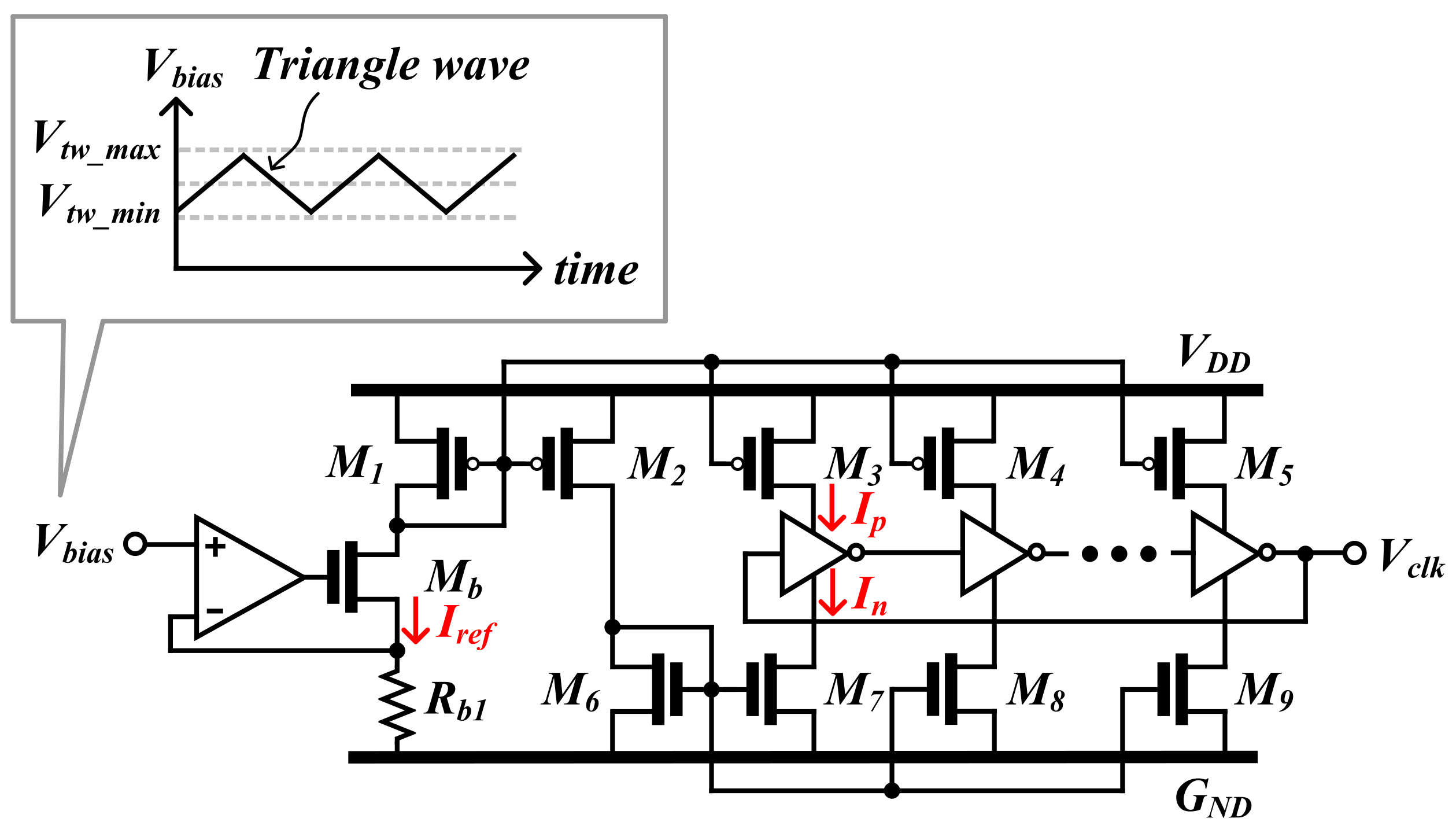
In this paper, an SSCG using a triangular wave modulation VCO is used to replace the clock generator shown in previous works. In the next paragraph, we will introduce and analyze the SSCG circuit.
Figure 2 shows the SSCG is implemented in the ring-oscillator topology VCO with triangular wave bias to achieve the simple circuit architecture with benefits of low power consumption and small design area. Although this structure is sensitive to PVT variations, it is easy to correct the frequency by adjusting V
bias. R
b1 is designed as a 100 kΩ chip resistor due to the advantage of resistors on a chip is that the chip area is small and the resistance is large. In
Figure 2, C
tot is the total output and input capacitances of a stage inverter. N is the stage of inverters in series. Assuming the inverter switching point voltage is about 0.5 V
DD, and the charging current I
p is equal to discharging current I
n, the rise time t
rise will equal to the fall time t
fall [
10]. If V
bias is a dc bias voltage, the oscillation frequency can be expressed by:
In
Figure 2, a continuous triangle-wave pattern is used to replace a dc bias voltage. The V
tw_max and V
tw_min are the peak and the valley voltage values of the continuous triangle wave, respectively. Thus, the bias current (I
ref) can be modulated, and the maximum/minimum bias current can be expressed as
In order to simplify the calculation, if the size of PMOS M1 is equal to M2, M3, M4, and M5 and the size of NMOS M6 are equal to M7, M8, and M9, Iref would be equal to Ip and In by current mirror. With I
ref_max and I
ref_min being substituted into Equation (2), the maximum/minimum oscillation frequency can be expressed as
In conclusion, we use a VCO with triangular wave bias to implement an SSCG, and the oscillation frequency is set between f
ref_max and f
ref_min. Therefore, triangular modulation frequency technology adopted in the regulated pulse current driver achieves spread spectrum. Because this driver produces a series of periodic pulse currents. In the following, we will introduce the parameter relationship of the periodic pulse signal demonstrated in the time domain and frequency domain, as shown in
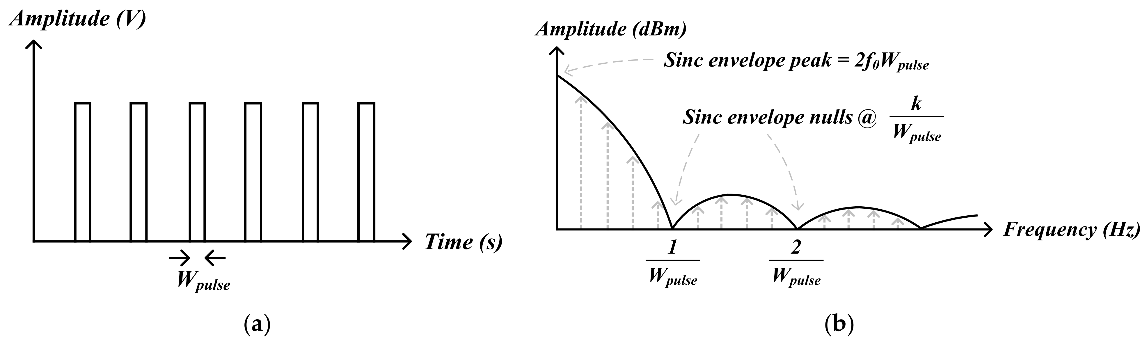
Figure 3a,b.
Figure 3b is the corresponding spectrum with a well-known Sinc(x) shaping waveform superimposed on the tonal spectrum [
11]. Thus, the frequency spectrum forms a Sinc function envelope, where the Sinc envelope peak can be expressed as
and the Sinc envelope nulls can be expressed as
where f
0 is the operation frequency of periodic pulse signal, W
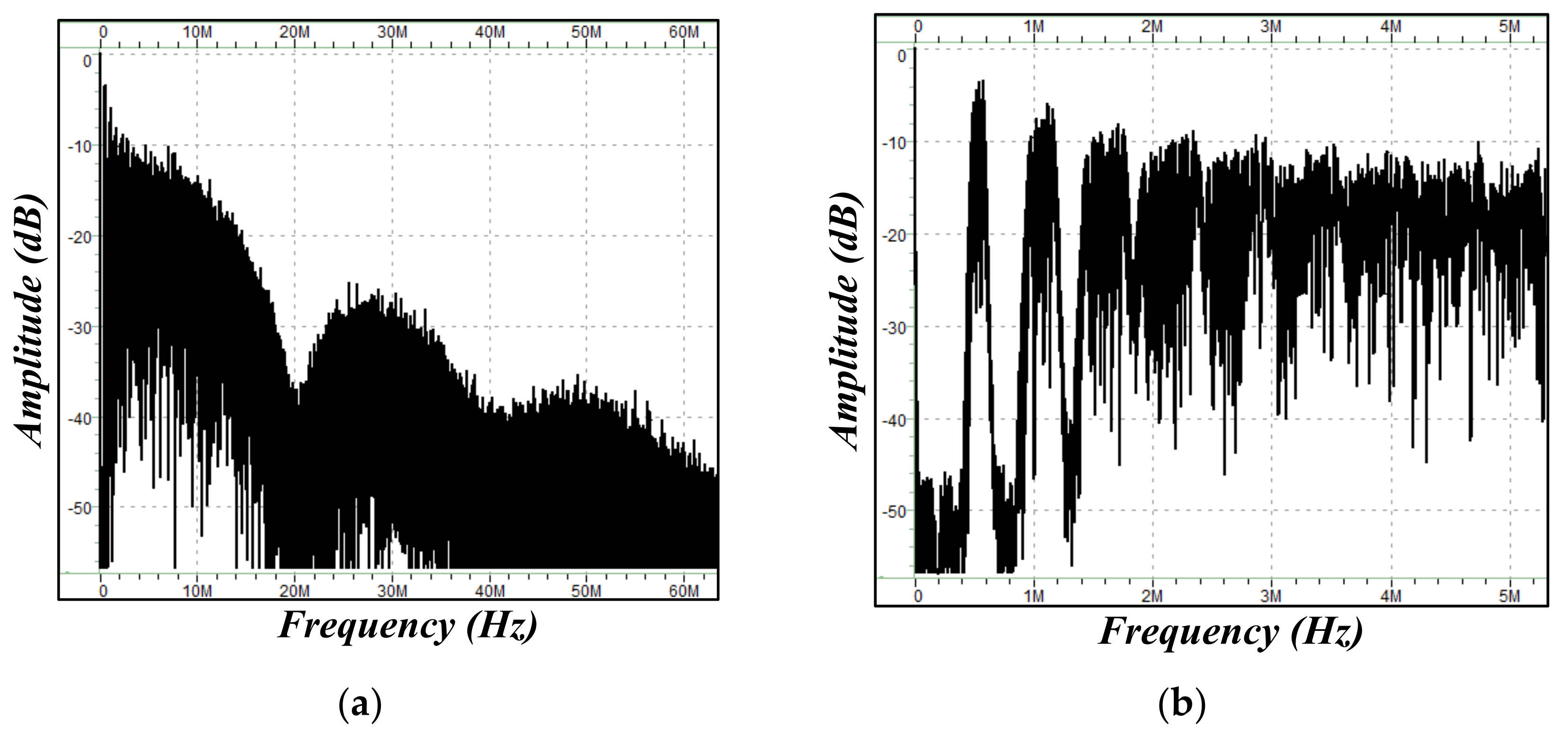
pulse is the pulse width of the periodic pulse signal, and k is a positive integer number. Moreover, observed from the above mathematical equations, the pulse width of the periodic pulse signal is proportional to the Sinc envelope peak and inversely proportional to the Sinc envelope nulls. In this driver with spread spectrum technique, the operating frequency will be modulated, but pulse width is fixed. In the frequency domain, envelope peak amplitude will be reduced, and envelope nulls are fixed. The above equation and conclusion will be used to help verify the simulation results and measurement results in the following sections.
3. Simulation Results of the Regulated Pulse Current Driver with SSCG
The regulated pulse current driver is simulated by the Hspice with VIS 0.5 μm 5 V CMOS process model.
Figure 4a shows a single pulse current with 50 ns pulse width and 300 mA peak current. The pulse current with 500 kHz operation frequency is shown in
Figure 4b.
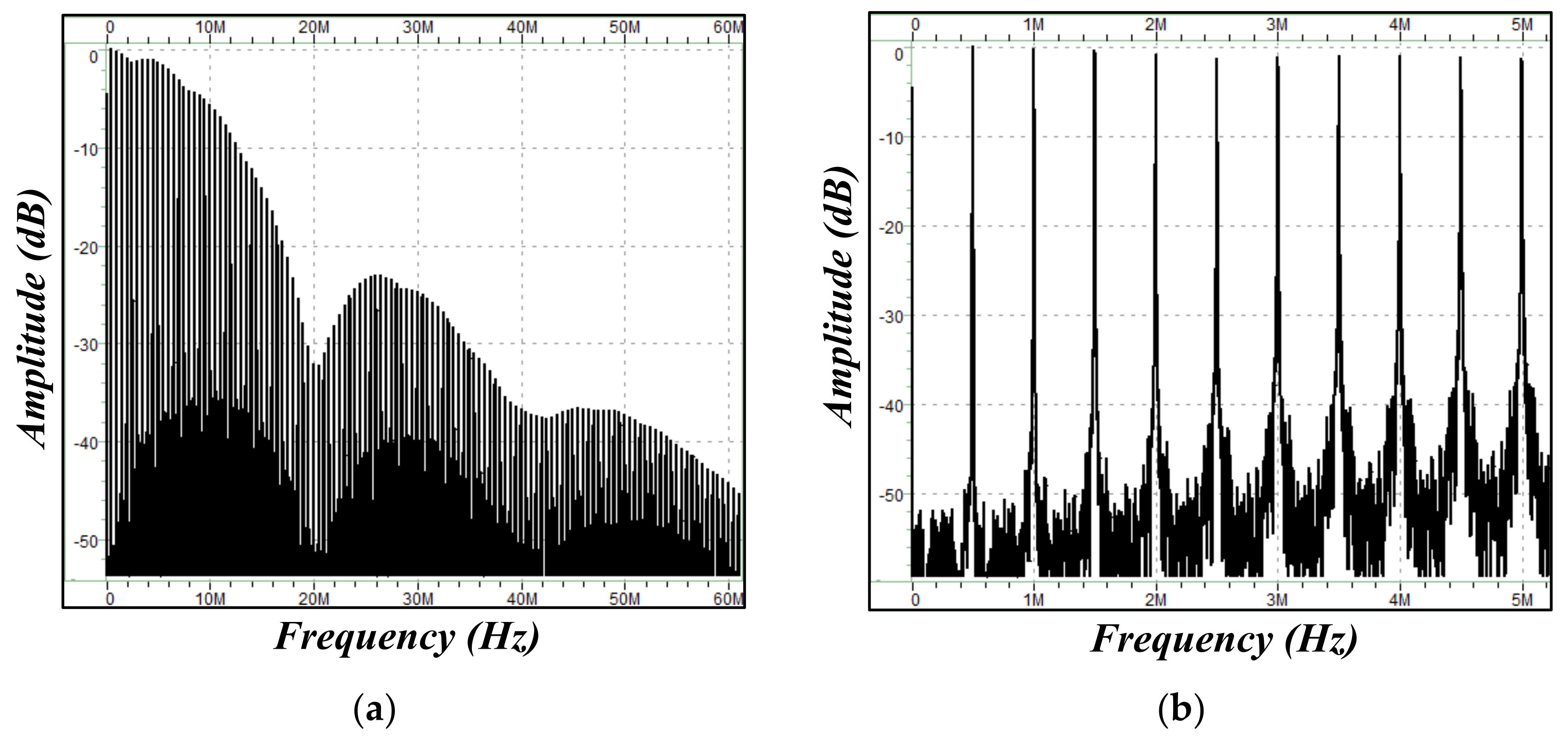
With the same operation frequency in
Figure 4b, the simulated spectrum results of the proposed driver are shown in
Figure 5a,b with spectral ranges of 60 MHz and 5 MHz, respectively. From
Figure 5a, the first envelope null is located at about 20 MHz that is corresponding to the reciprocal of pulse width in
Figure 4a. In addition, from Equation (8), the first null location can be calculated as
We zoom in
Figure 5a to get
Figure 5b with a spectral range up to 5 MHz.
Figure 5b demonstrates the operation frequency at 500 kHz, and the second harmonic at 1 MHz, and so on.
Big spread ratio makes big EMI reduction, but it is harmful to the clock purity [
4]. Moreover, the maximum deviation of the clock frequency is decided by the linearity region of the bias voltage versus clock frequency. In the following simulation condition, the operation frequency of pulse current fc is set as 500 kHz. The frequency modulation variation ∆fc is designed at 50 kHz. Triangular modulation frequency fm is designed at 10 kHz. ∆fc/fc is ±10%. The operation frequency of pulse current is approximately set at 500 kHz ± 50 kHz.
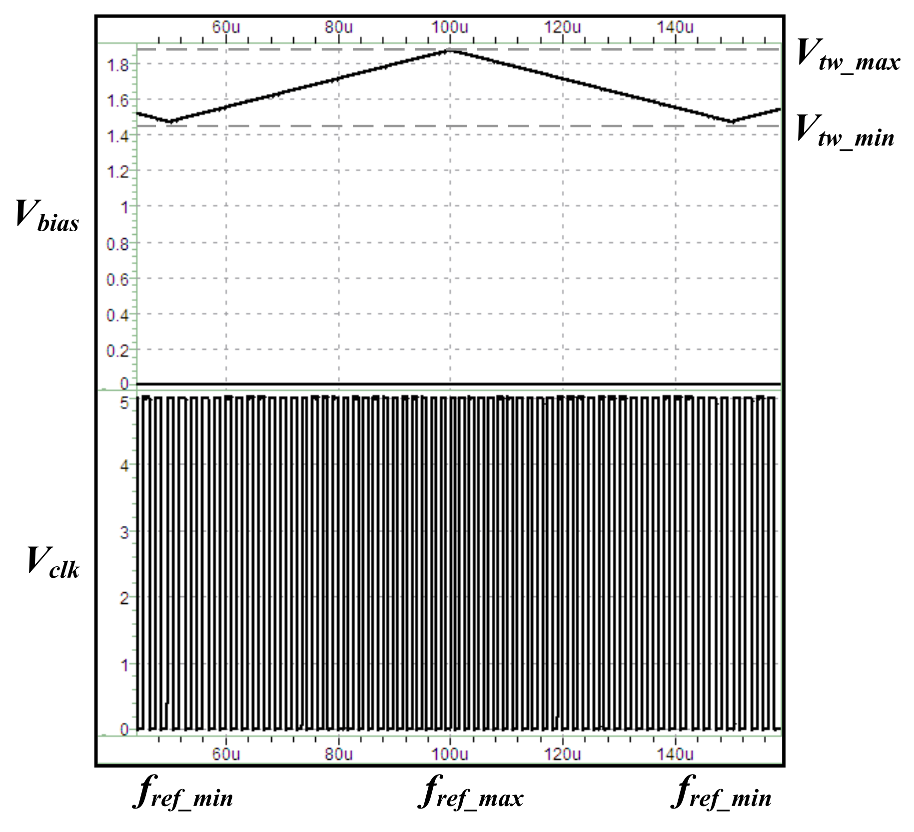
Figure 6 shows the simulation result of the triangle-wave bias voltage corresponding to the clock frequency of the SSCG. The amplitude of the triangle pattern is 200 mV, and the maximum bias voltage (V
tw_max) and minimum bias voltage (V
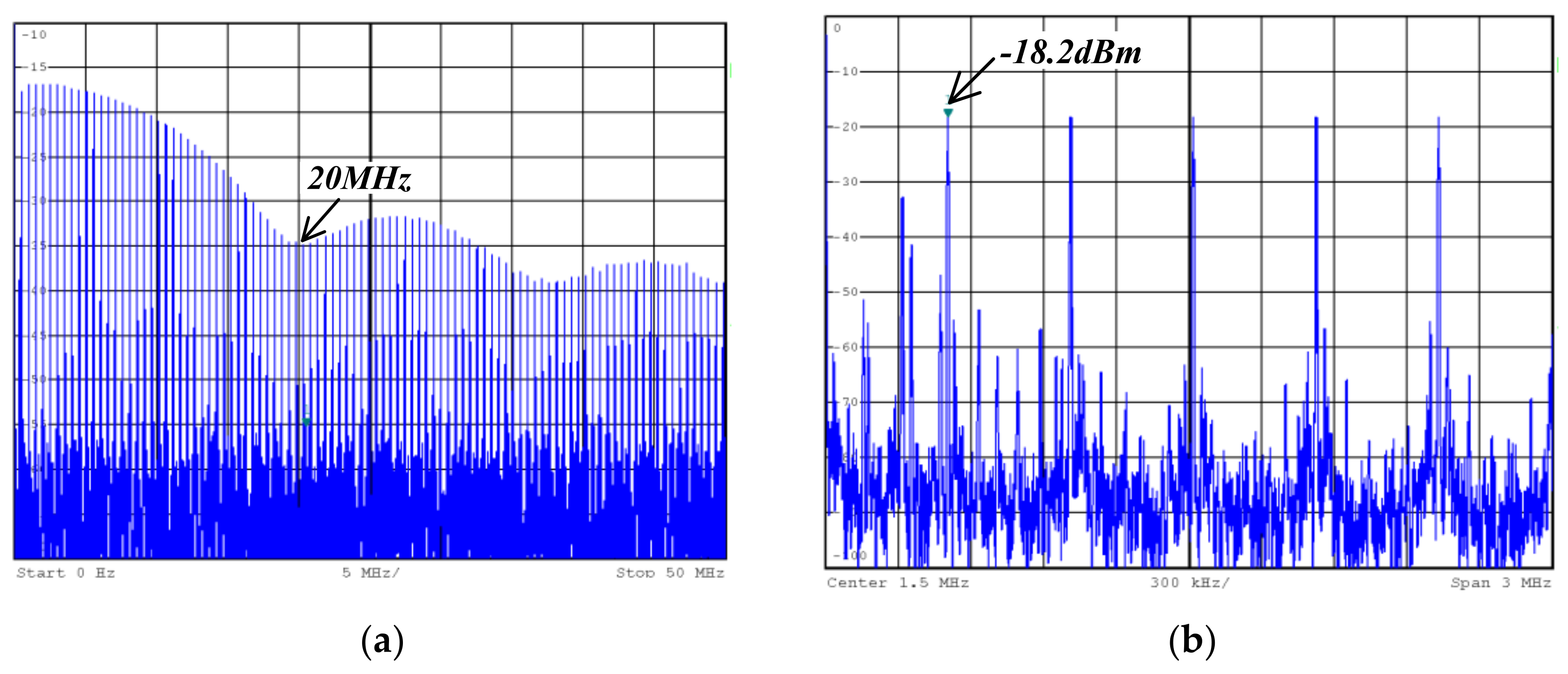
tw_min) are about 1.87 V and 1.47 V, respectively. Therefore, the output clock frequency of the SSCG with triangle-wave bias would be modulated between 450 and 550 kHz. The simulated spectrum results of the pulse current driver with SSCG are shown in
Figure 7a,b, whose spectral ranges are 60 MHz and 5 MHz, respectively.
As observed from
Figure 7a, the first envelope null is also located at about 20 MHz, which is the same as shown in
Figure 5a, which verifies Equation (8). We zoom in
Figure 7a to get
Figure 7b with a spectral range up to 5 MHz.
Figure 7b demonstrates that the operation frequency is modulated between 450 and 550 kHz, and the peak power is reduced by 3 dB from that of
Figure 5b, which verifies the feasibility of the topology.
The regulated pulse current driver comes with closed-loop control, and thus it can regulate pulse current amplitude by adjusting amplitude control signal (Vref) and modulate pulse current frequency by adjusting the output clock frequency of the SSCG. Moreover, this driver is also attached with the spread spectrum technique to disperse the energy in the frequency band to lower the EMI effect for commercial products. According to the simulated results, the feasibility of the driver’s architecture is demonstrated.
4. Measurement Results of the Regulated Pulse Current Driver with SSCG
The pulse width is related to the bandwidth of this driver. In this work, 50 ns is the shortest pulse width at a pulse current amplitude of 200 mA. The pulse current is about 50 ns pulse width, 500 kHz operation frequency, and
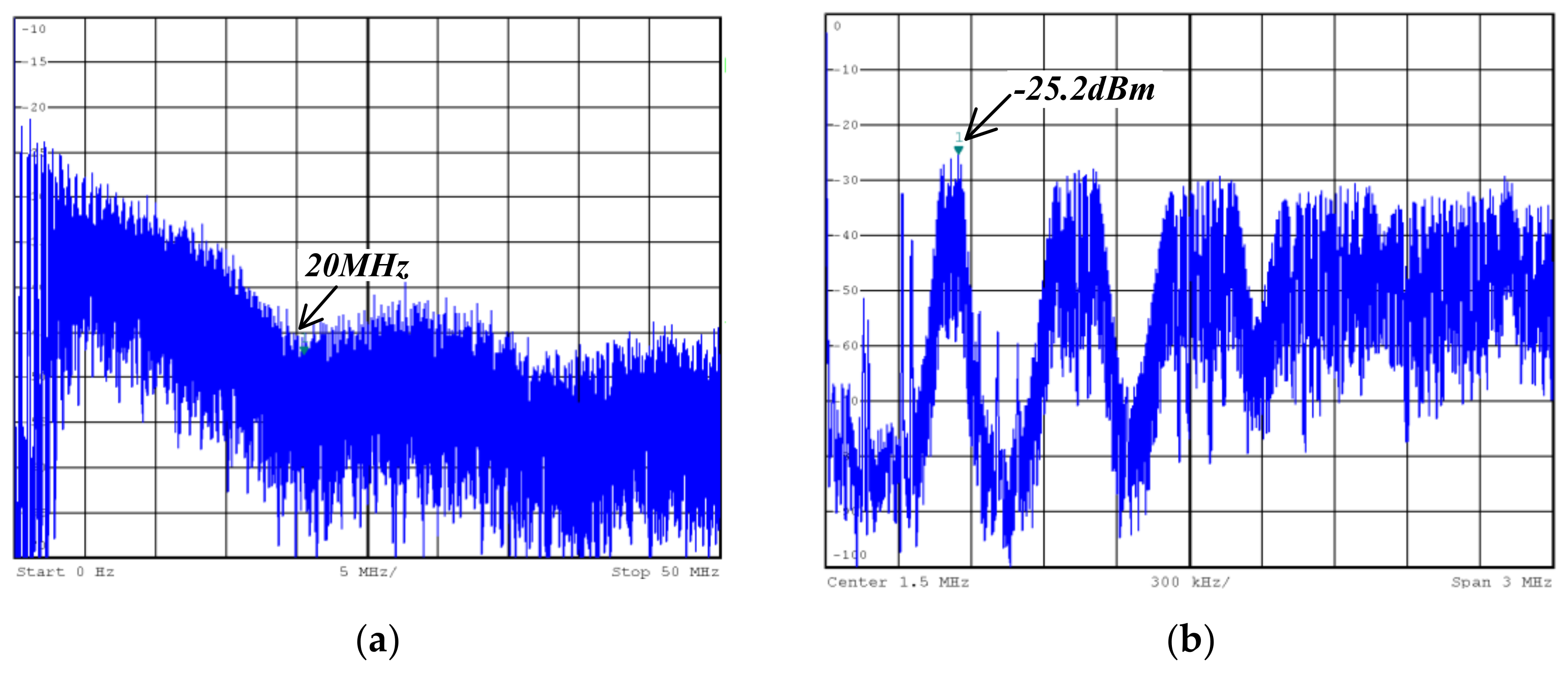
Figure 8a,b are the spectral measurement results of pulse voltage that spectral ranges are within 50 MHz and 3 MHz, respectively. As observed from
Figure 8a, the first envelope null is located at about 20 MHz that is approximately proportional to the reciprocal of the pulse width. We zoom in
Figure 8a to get
Figure 8b with a spectral range up to 3 MHz.
Figure 8b demonstrates that the operation frequency of pulse current is about 500 kHz, and the second harmonic is at about 1 MHz, and so on. The measurement results shown in
Figure 8 are consistent with the simulation results in
Figure 5.
Figure 9 is the measurement result of the triangle-wave bias voltage corresponding to the pulse current. From top to bottom, shown in
Figure 9, the waveforms are the bias voltage V
bias of the SSCG circuit and the pulse current I
pulse, respectively. The amplitude of the triangle wave is about 200 mV, and the maximum and minimum bias voltages are about 1.87 and 1.47 V, respectively. The triangular modulation frequency of V
bias is 10 kHz. The operation frequency of the pulse current is modulated between 450 and 550 kHz.
The spectral measurement results of the regulated pulse current driver with SSCG are shown in
Figure 10a,b with the spectral range of 50 and 3 MHz, respectively. From
Figure 10a, the first envelope null is located at about 20 MHz, and it is the same as the one shown in
Figure 8a. We zoom in
Figure 10a to get
Figure 10b with a spectral range up to 3 MHz.
Figure 10b demonstrates the operation frequency is modulated between 450 and 550 kHz, and the peak power is reduced by 7 dBm from that of
Figure 8b. The measurement results shown in
Figure 10 are not only consistent with the simulation results in
Figure 7 but also verify the feasibility of the structure and the performance of this topology.
Detailed specifications of the regulated pulse current driver with SSCG are listed in
Table 1. This driver is applied to consumer electronics; therefore, we use 0.5 μm CMOS process implementation to achieve lower cost.
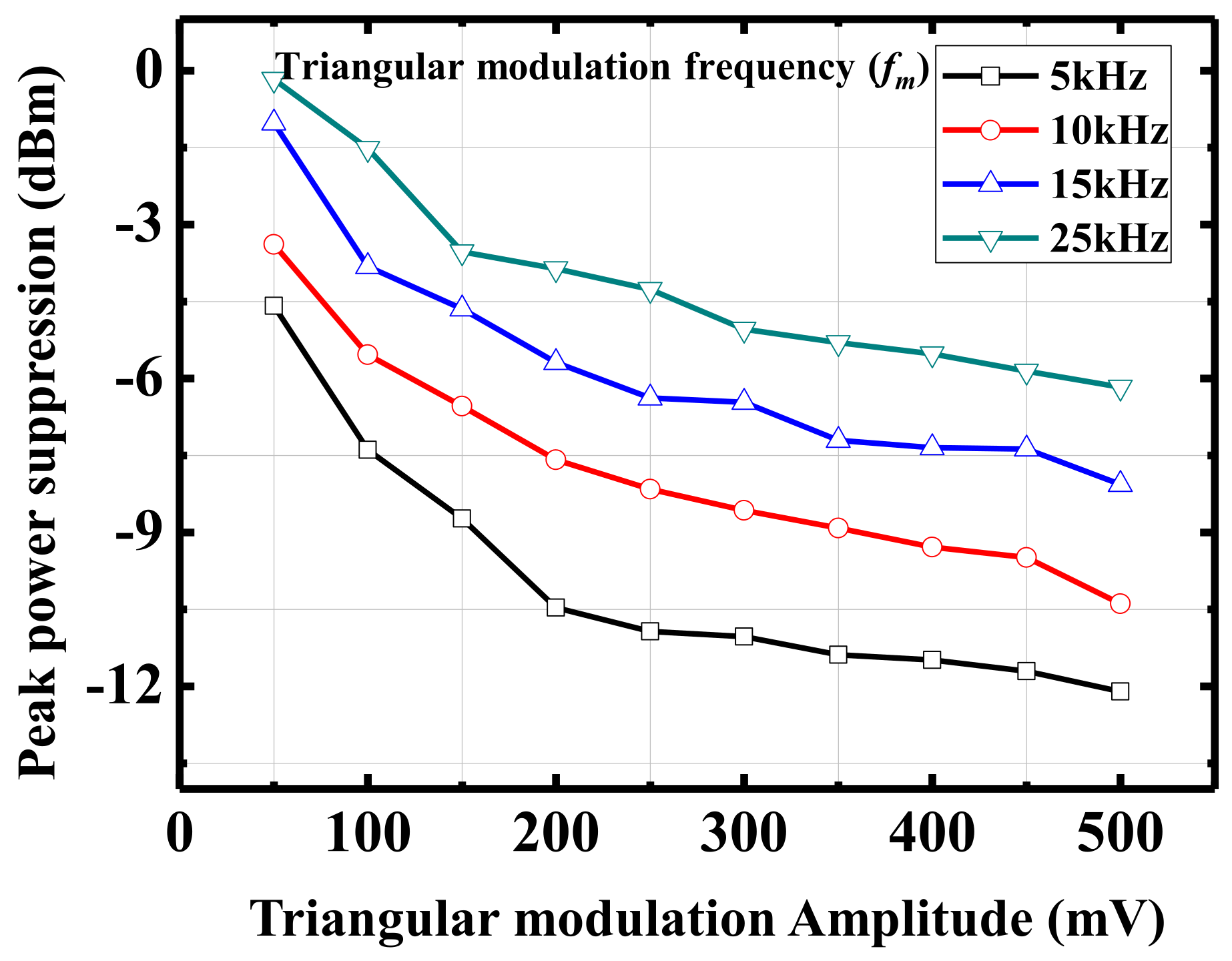
Figure 11 summarizes spectral measurement results of the peak power suppression with difference triangular modulation amplitude and frequency.
Figure 11 shows that a triangular pattern with amplitude ranges from 50 to 500 mV and shows the lower fm frequency with the more peak power suppression in the same frequency modulation variation. This driver with the triangle-wave amplitude at 500 mV and triangle modulation frequency at 5 kHz provides a maximum of up to 12 dBm peak power reduction.
Table 2 illustrates the performance comparison for different spread spectrum techniques. This work uses a relatively backward process to achieve low power consumption with the same level of EMI reduction.


