
Radiation-Tolerant All-Digital PLL/CDR with Varactorless LC DCO in 65 nm CMOS

 , , ,
, , ,  and
and
Abstract
:1. Introduction
2. Radiation Effects in Conventional PLL Designs
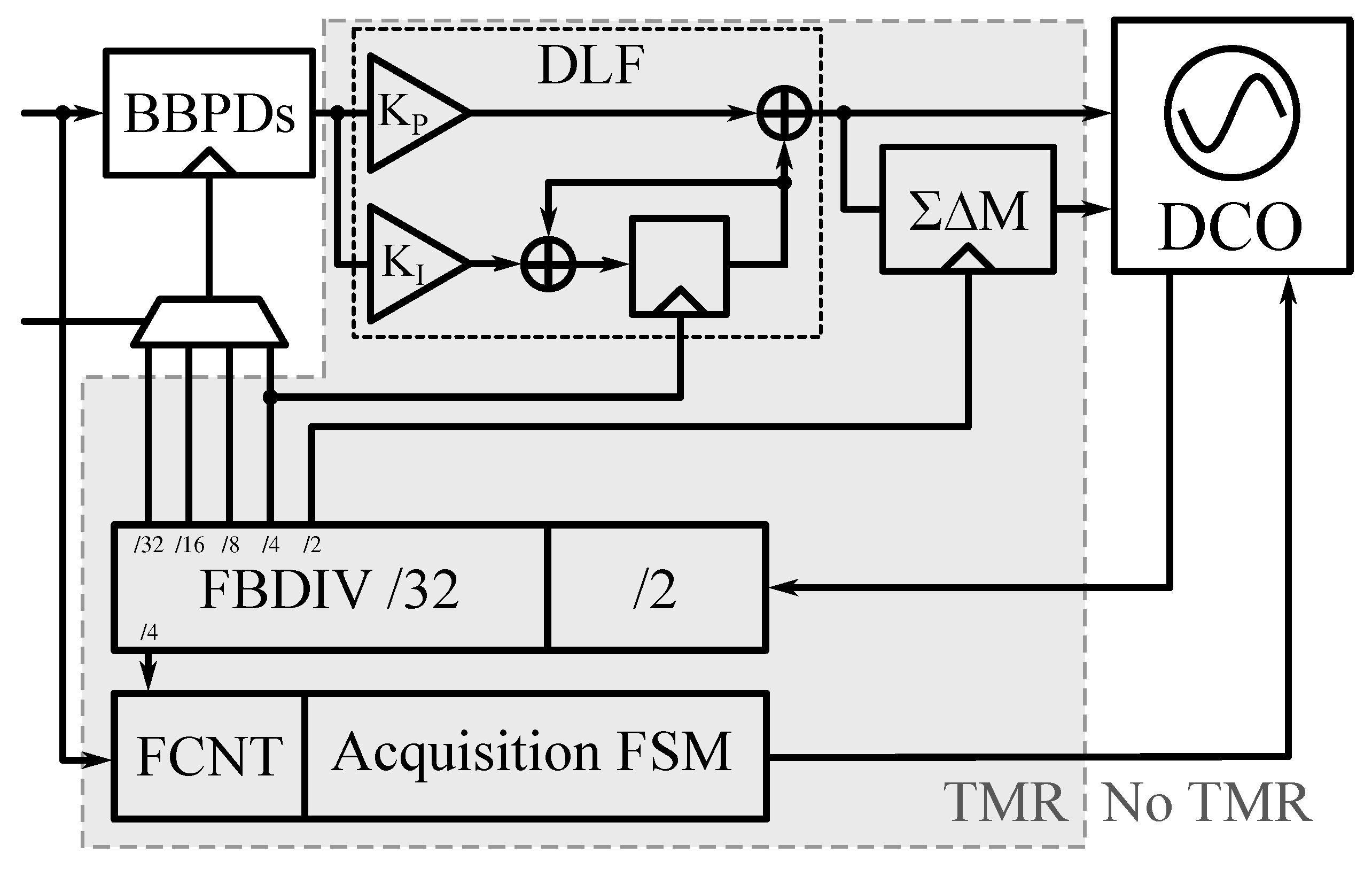
3. Radiation-Tolerant All-Digital PLL and CDR Architecture
4. Implementation
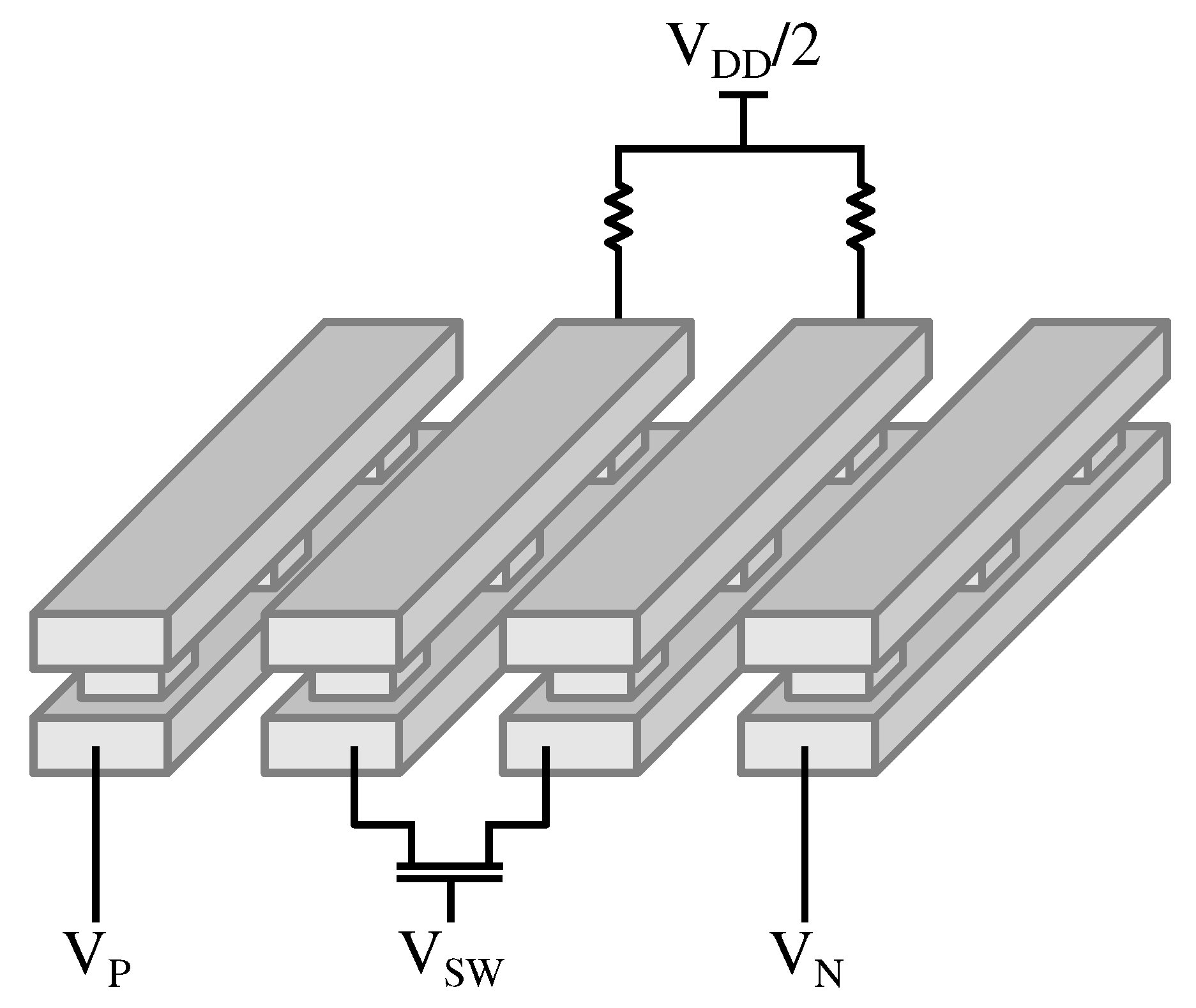
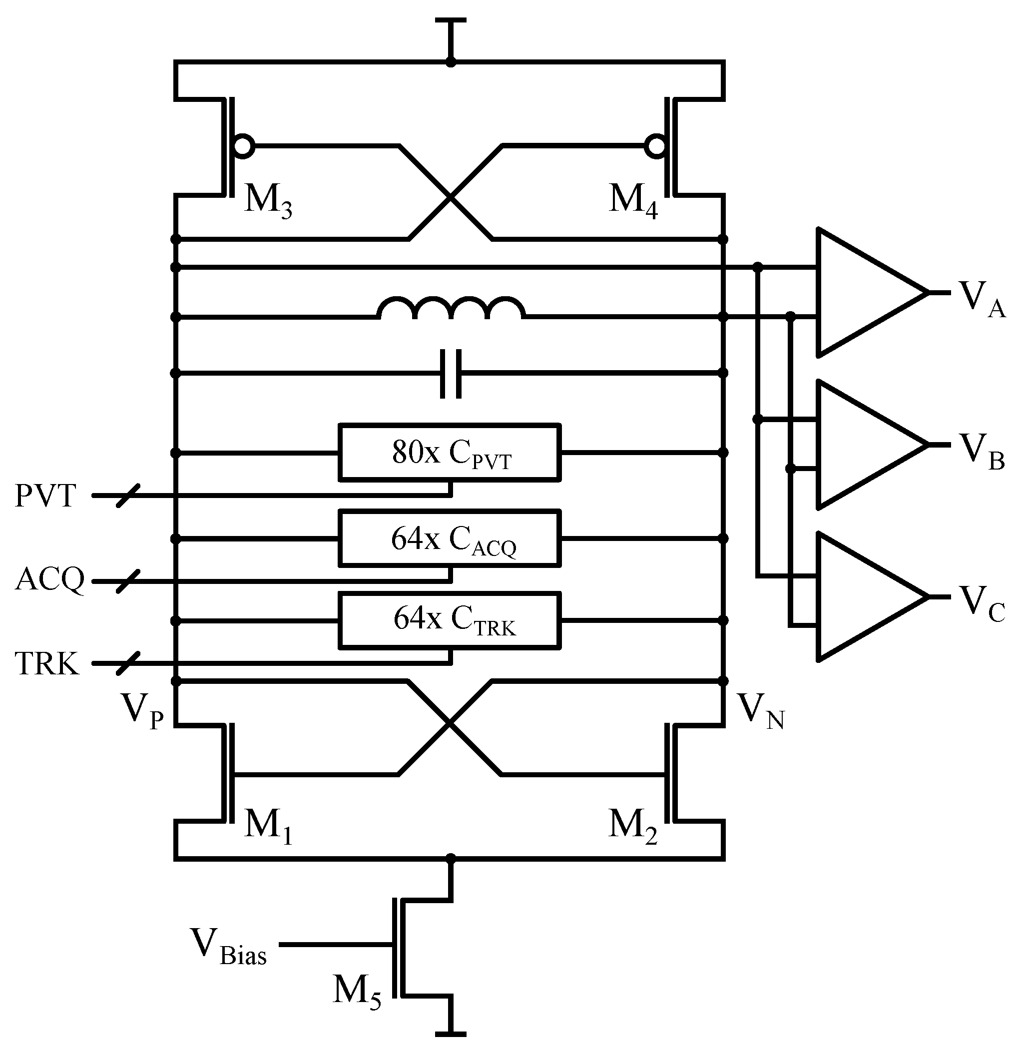
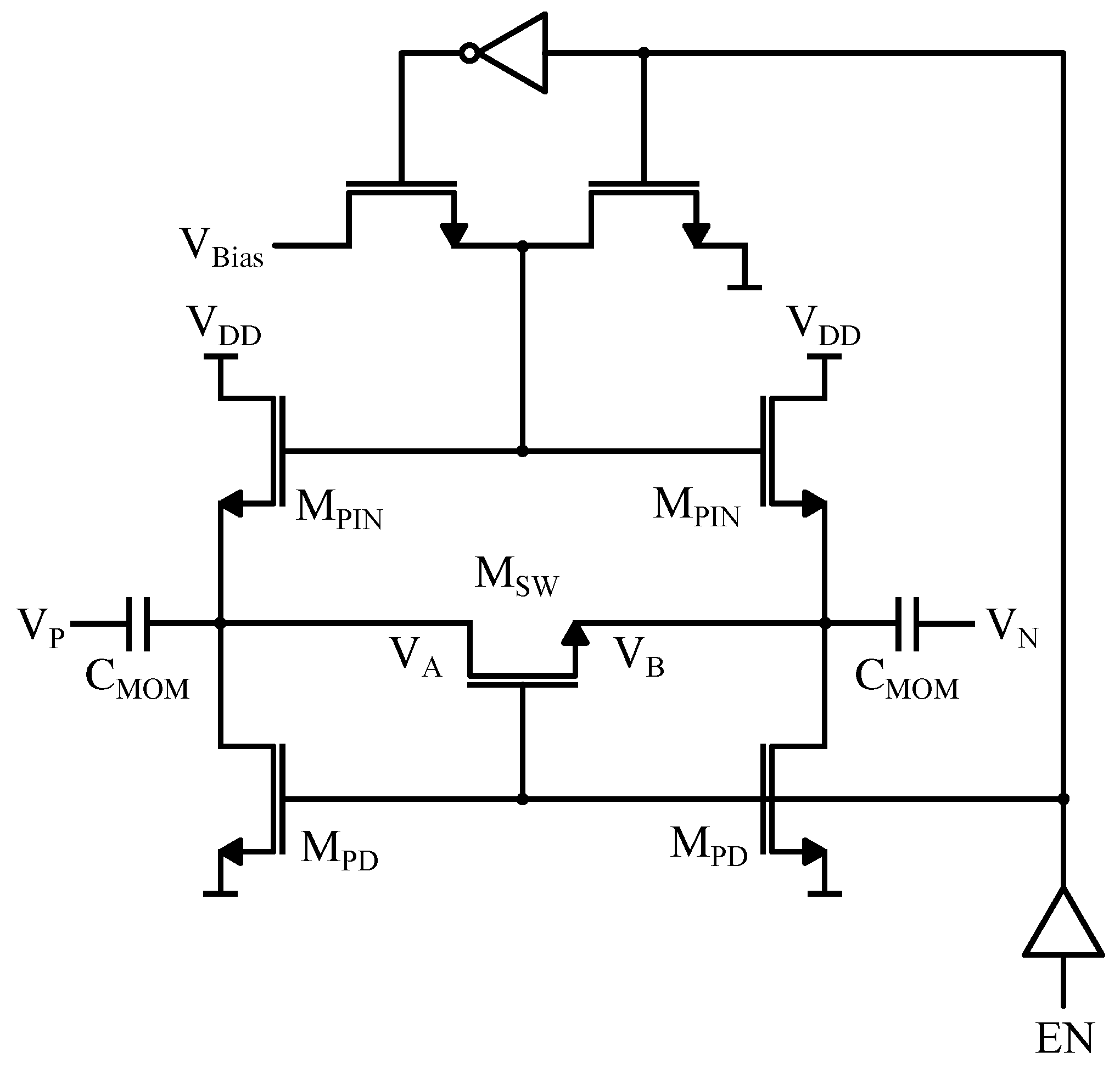
4.1. LC DCO
4.2. Divide-by-Two Prescaler
4.3. Clocking and Clock Distribution
4.4. Digital Loop
5. Measurements
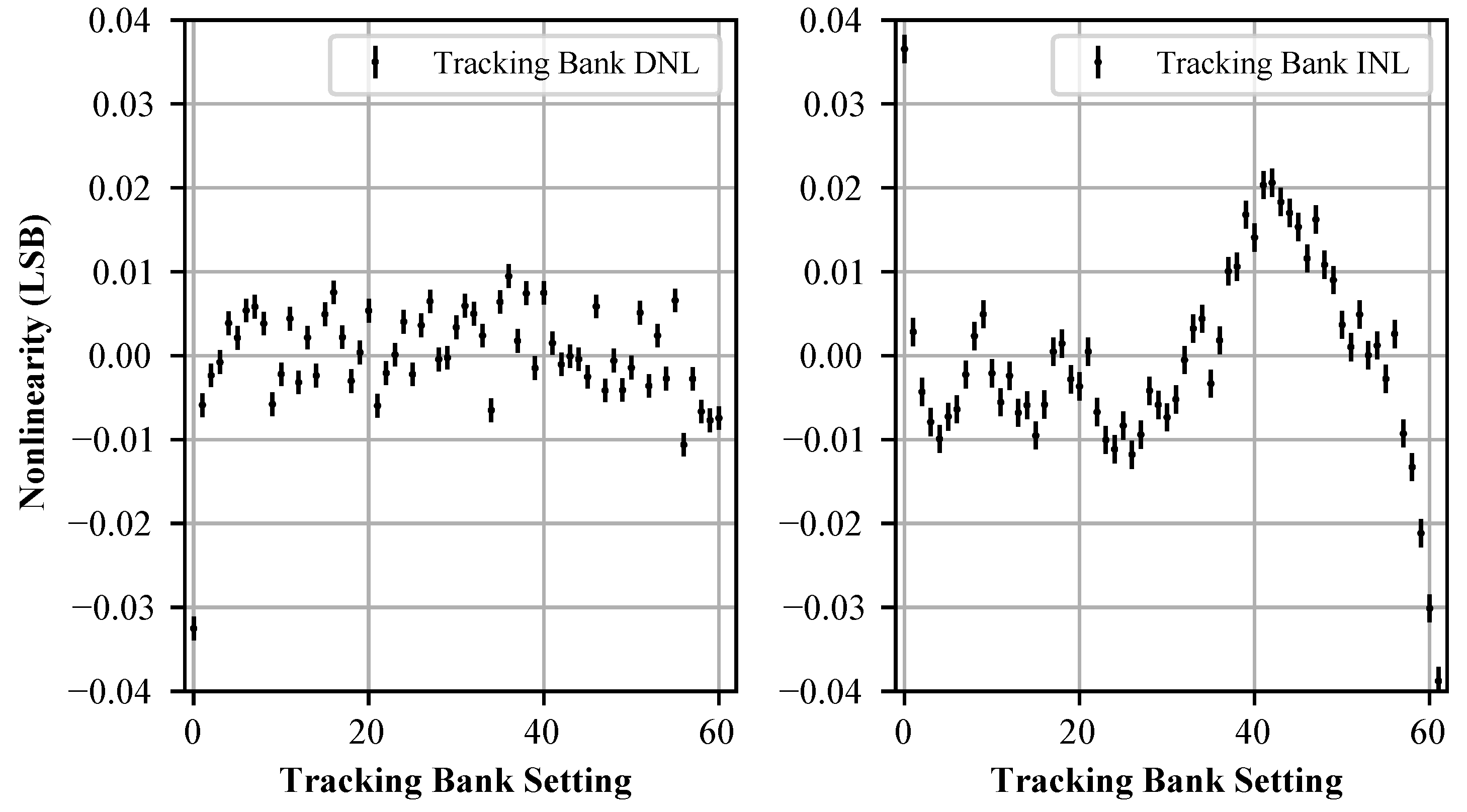
5.1. DCO Characterization
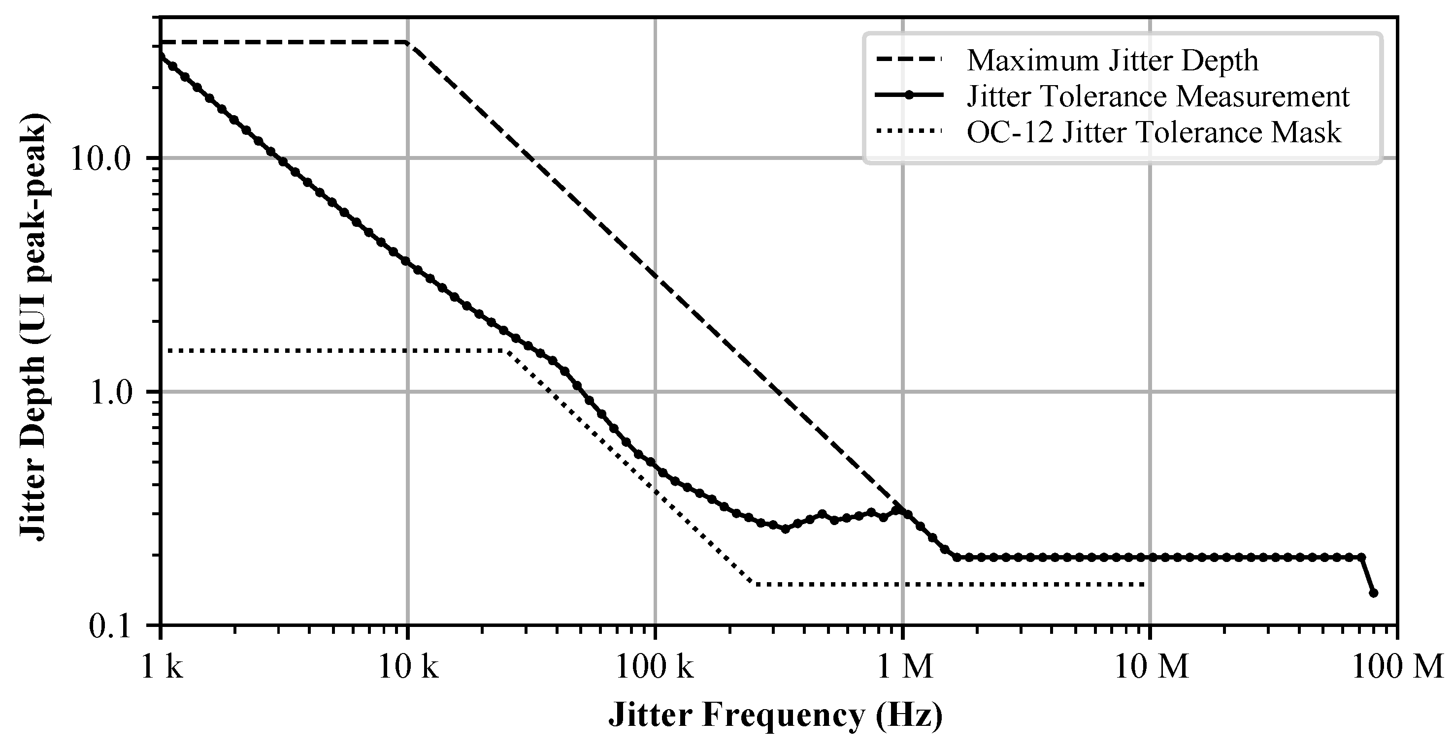
5.2. PLL and CDR Performance
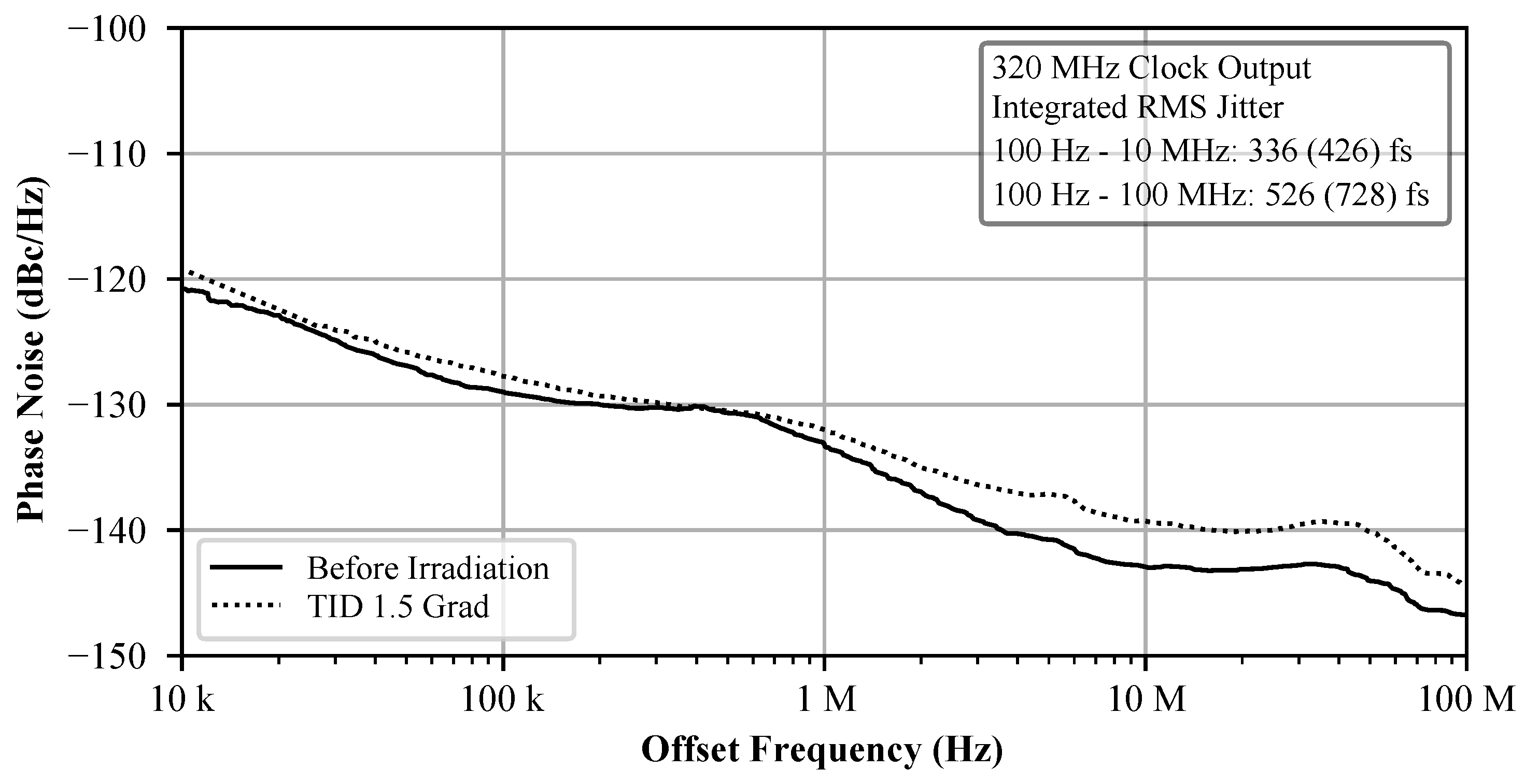
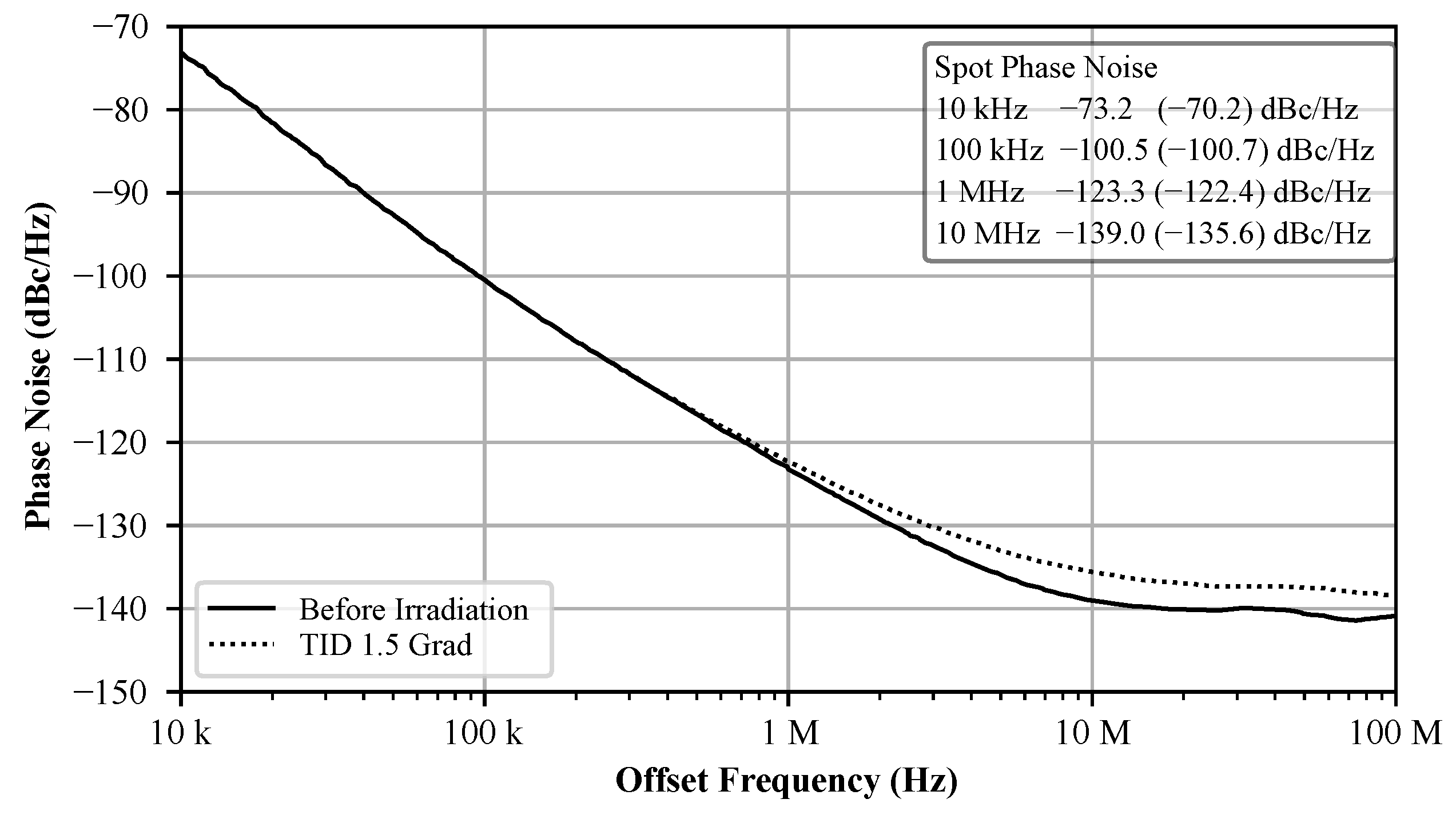
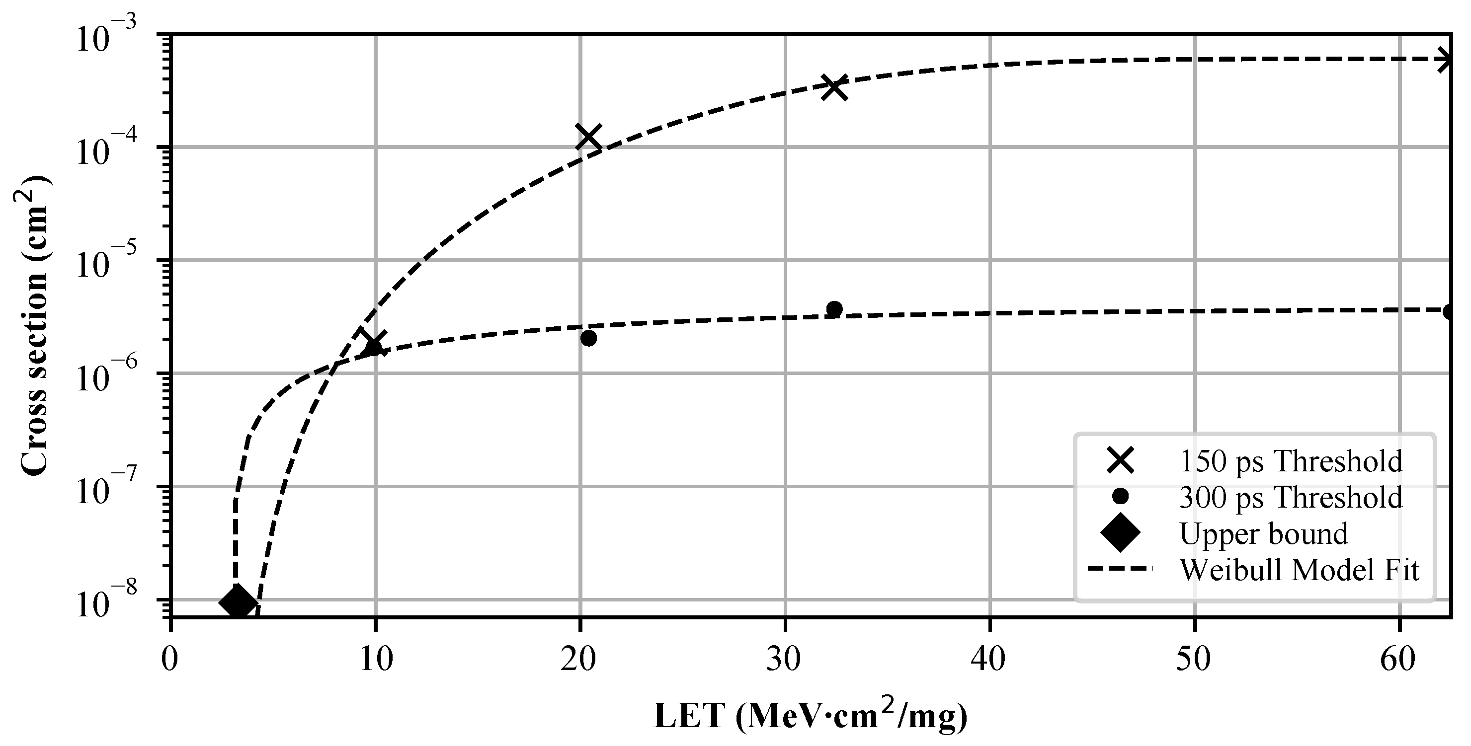
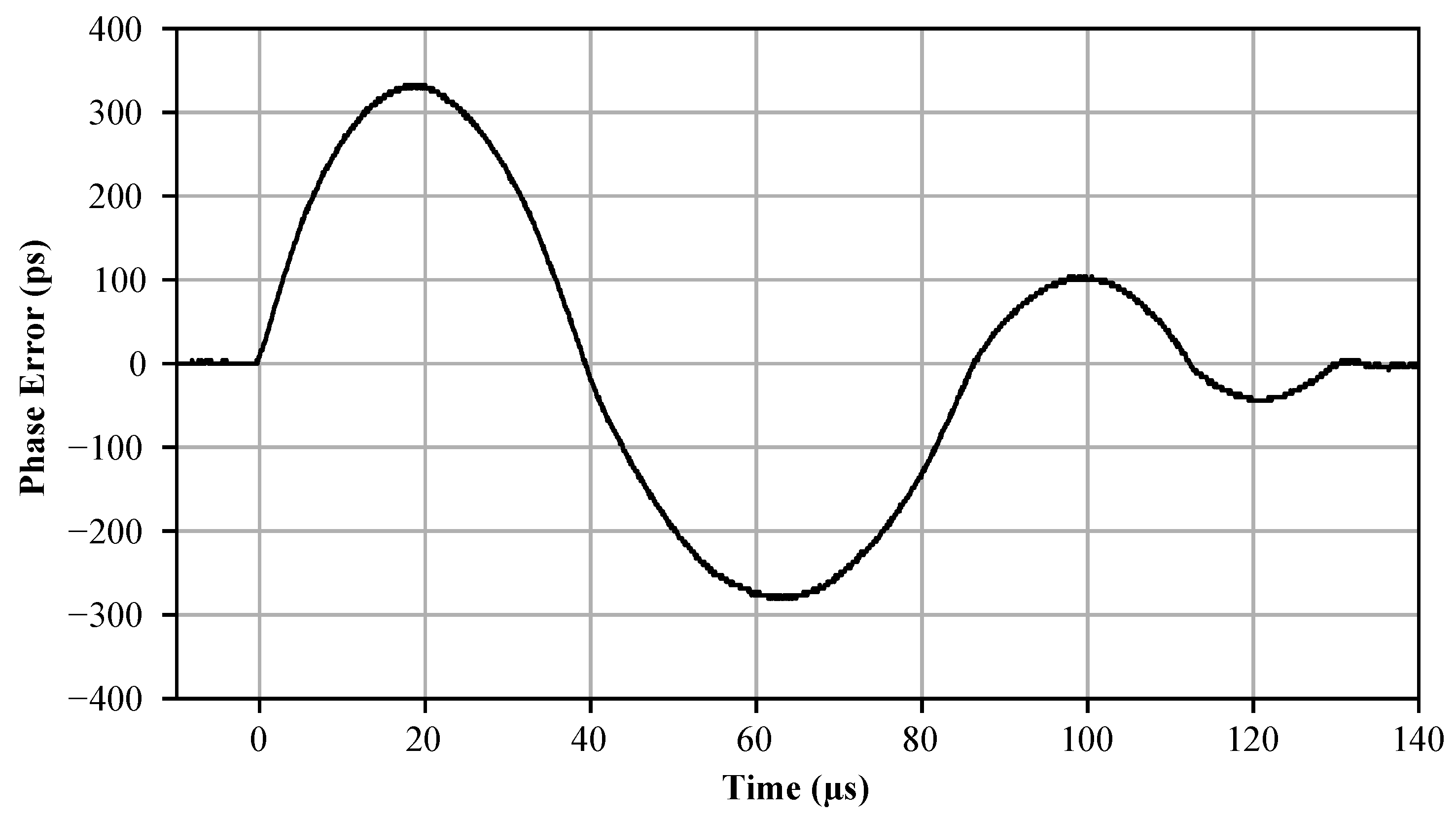
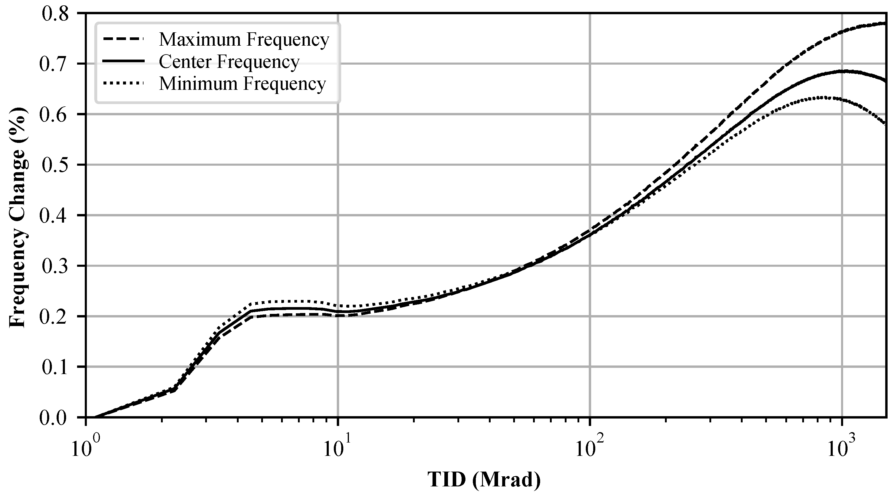
5.3. Radiation Testing
5.4. Summary
6. Conclusions
Author Contributions
Funding
Acknowledgments
Conflicts of Interest
References
- ATLAS Collaboration. Technical Design Report: A High-Granularity Timing Detector for the ATLAS Phase-II Upgrade; Technical Report; CERN: Geneva, Switzerland, 2020. [Google Scholar]
- SpaceFibre—Very High-Speed Serial Link; Standard; European Cooperation for Space Standardization: Noordwijk, NL, USA, 2019.
- Orfanelli, S. The Phase 2 Upgrade of the CMS Inner Tracker. Nucl. Instrum. Meth. A 2020, 980, 164396. [Google Scholar] [CrossRef]
- Mavis, D.; Eaton, P. Soft error rate mitigation techniques for modern microcircuits. In Proceedings of the 2002 IEEE International Reliability Physics Symposium. Proceedings. 40th Annual (Cat. No.02CH37320), Dallas, TX, USA, 7–11 April 2002; pp. 216–225. [Google Scholar] [CrossRef]
- Staszewski, R.; Wallberg, J.; Rezeq, S.; Hung, C.M.; Eliezer, O.; Vemulapalli, S.; Fernando, C.; Maggio, K.; Staszewski, R.; Barton, N.; et al. All-digital PLL and transmitter for mobile phones. IEEE J. Solid-State Circuits 2005, 40, 2469–2482. [Google Scholar] [CrossRef]
- Johnston, A. Radiation effects in advanced microelectronics technologies. IEEE Trans. Nucl. Sci. 1998, 45, 1339–1354. [Google Scholar] [CrossRef] [Green Version]
- Prinzie, J.; Steyaert, M.; Leroux, P.; Christiansen, J.; Moreira, P. A single-event upset robust, 2.2 GHz to 3.2 GHz, 345 fs jitter PLL with triple-modular redundant phase detector in 65 nm CMOS. In Proceedings of the 2016 IEEE Asian Solid-State Circuits Conference (A-SSCC), Toyama, Japan, 7–9 November 2016; pp. 285–288. [Google Scholar] [CrossRef]
- Loveless, T.D.; Massengill, L.W.; Holman, W.T.; Bhuva, B.L.; McMorrow, D.; Warner, J.H. A Generalized Linear Model for Single Event Transient Propagation in Phase-Locked Loops. IEEE Trans. Nucl. Sci. 2010, 57, 2933–2947. [Google Scholar] [CrossRef]
- Biereigel, S.; Kulis, S.; Leitao, P.; Francisco, R.; Moreira, P.; Leroux, P.; Prinzie, J. A Low Noise Fault Tolerant Radiation Hardened 2.56 Gbps Clock-Data Recovery Circuit With High Speed Feed Forward Correction in 65 nm CMOS. IEEE Trans. Circuits Syst. I Regul. Pap. 2020, 67, 1438–1446. [Google Scholar] [CrossRef]
- Jung, S.M.; Roveda, J.M. A radiation-hardened-by-design phase-locked loop using feedback voltage controlled oscillator. In Proceedings of the Sixteenth International Symposium on Quality Electronic Design, Santa Clara, CA, USA, 2–4 March 2015; pp. 103–106. [Google Scholar] [CrossRef]
- Boulghassoul, Y.; Massengill, L.W.; Steinberg, A.L.; Bhuva, B.L.; Holman, W.T. Towards SET Mitigation in RF Digital PLLs: From Error Characterization to Radiation Hardening Considerations. IEEE Trans. Nucl. Sci. 2006, 53, 2047–2053. [Google Scholar] [CrossRef]
- Loveless, T.D.; Massengill, L.W.; Bhuva, B.L.; Holman, W.T.; Witulski, A.F.; Boulghassoul, Y. A Hardened-by-Design Technique for RF Digital Phase-Locked Loops. IEEE Trans. Nucl. Sci. 2006, 53, 3432–3438. [Google Scholar] [CrossRef]
- Loveless, T.D.; Massengill, L.W.; Bhuva, B.L.; Holman, W.T.; Reed, R.A.; McMorrow, D.; Melinger, J.S.; Jenkins, P. A Single-Event-Hardened Phase-Locked Loop Fabricated in 130 nm CMOS. IEEE Trans. Nucl. Sci. 2007, 54, 2012–2020. [Google Scholar] [CrossRef]
- Gao, Y.; Lou, J.; Zhang, J.; Li, L.; Xu, F. Single-event transients in LC-tank VCO. In Proceedings of the 2012 International Workshop on Microwave and Millimeter Wave Circuits and System Technology, Chengdu, China, 19–20 April 2012; pp. 1–4. [Google Scholar] [CrossRef]
- Zhang, Z.; Chen, L.; Djahanshahi, H. A Hardened-By-Design Technique for LC-Tank Voltage Controlled Oscillator. In Proceedings of the 2018 IEEE Canadian Conference on Electrical Computer Engineering (CCECE), Quebec, QC, Canada, 13–16 May 2018; pp. 1–4. [Google Scholar] [CrossRef]
- Prinzie, J.; Christiansen, J.; Moreira, P.; Steyaert, M.; Leroux, P. Comparison of a 65 nm CMOS Ring- and LC-Oscillator Based PLL in Terms of TID and SEU Sensitivity. IEEE Trans. Nucl. Sci. 2017, 64, 245–252. [Google Scholar] [CrossRef]
- Chen, Y.P.; Massengill, L.W.; Bhuva, B.L.; Holman, W.T.; Loveless, T.D.; Robinson, W.H.; Gaspard, N.J.; Witulski, A.F. Single-Event Characterization of Bang-bang All-digital Phase-locked Loops (ADPLLs). IEEE Trans. Nucl. Sci. 2015, 62, 2650–2656. [Google Scholar] [CrossRef]
- Chen, Y.P.; Massengill, L.W.; Kauppila, J.S.; Bhuva, B.L.; Holman, W.T.; Loveless, T.D. Single-Event Upset Characterization of Common First- and Second-Order All-Digital Phase-Locked Loops. IEEE Trans. Nucl. Sci. 2017, 64, 2144–2151. [Google Scholar] [CrossRef]
- Chen, Y.P.; Massengill, L.W.; Sternberg, A.L.; Zhang, E.X.; Kauppila, J.S.; Yao, M.; Amort, A.L.; Bhuva, B.L.; Holman, W.T.; Loveless, T.D. Time-Domain Modeling of All-Digital PLLs to Single-Event Upset Perturbations. IEEE Trans. Nucl. Sci. 2018, 65, 311–317. [Google Scholar] [CrossRef]
- Alexander, J. Clock recovery from random binary signals. Electron. Lett. 1975, 11, 541–542. [Google Scholar] [CrossRef]
- Staszewski, R.; Hung, C.M.; Barton, N.; Lee, M.C.; Leipold, D. A digitally controlled oscillator in a 90 nm digital CMOS process for mobile phones. IEEE J. Solid-State Circuits 2005, 40, 2203–2211. [Google Scholar] [CrossRef]
- Xu, Z.; Miyahara, M.; Okada, K.; Matsuzawa, A. A 3.6 GHz Low-Noise Fractional-N Digital PLL Using SAR-ADC-Based TDC. IEEE J. Solid-State Circuits 2016, 51, 2345–2356. [Google Scholar] [CrossRef]
- Kuo, F.W.; Babaie, M.; Chen, H.N.R.; Cho, L.C.; Jou, C.P.; Chen, M.; Staszewski, R.B. An All-Digital PLL for Cellular Mobile Phones in 28-nm CMOS with -55 dBc Fractional and -91 dBc Reference Spurs. IEEE Trans. Circuits Syst. I Regul. Pap. 2018, 65, 3756–3768. [Google Scholar] [CrossRef]
- Bonfanti, A.; Levantino, S.; Samori, C.; Lacaita, A. A varactor configuration minimizing the amplitude-to-phase noise conversion in VCOs. IEEE Trans. Circuits Syst. I Regul. Pap. 2006, 53, 481–488. [Google Scholar] [CrossRef]
- Bonacini, S.; Valerio, P.; Avramidou, R.; Ballabriga, R.; Faccio, F.; Kloukinas, K.; Marchioro, A. Characterization of a commercial 65 nm CMOS technology for SLHC applications. J. Instrum. 2012, 7, P01015. [Google Scholar] [CrossRef]
- Hershberg, B.; Raczkowski, K.; Vaesen, K.; Craninckx, J. A 9.1–12.7 GHz VCO in 28nm CMOS with a bottom-pinning bias technique for digital varactor stress reduction. In Proceedings of the ESSCIRC 2014—40th European Solid State Circuits Conference (ESSCIRC), Venice Lido, Italy, 22–26 September 2014; pp. 83–86. [Google Scholar] [CrossRef]
- Nikolaou, A.; Bucher, M.; Makris, N.; Papadopoulou, A.; Chevas, L.; Borghello, G.; Koch, H.D.; Faccio, F. Modeling of High Total Ionizing Dose (TID) Effects for Enclosed Layout Transistors in 65 nm Bulk CMOS. In Proceedings of the 2018 International Semiconductor Conference (CAS), Sinaia, Romania, 10–12 October 2018; pp. 133–136. [Google Scholar] [CrossRef]
- Kulis, S. Single Event Effects mitigation with TMRG tool. J. Instrum. 2017, 12, C01082. [Google Scholar] [CrossRef] [Green Version]
- Jara Casas, L.M. DRAD Results Obtained during Irradiation Campaigns; Technical Report; CERN: Geneva, Switzerland, 2020. [Google Scholar]
- Biereigel, S.; Kulis, S.; Leroux, P.; Moreira, P.; Kölpin, A.; Prinzie, J. Single-Event Effect Responses of Integrated Planar Inductors in 65 nm CMOS. IEEE Trans. Nucl. Sci. 2021. [Google Scholar] [CrossRef]
- Huhtinen, M.; Faccio, F. Computational method to estimate single event upset rates in an accelerator environment. Nucl. Instrum. Meth. A 2000, 450, 155–172. [Google Scholar] [CrossRef]
- Sjoland, H. Improved switched tuning of differential CMOS VCOs. IEEE Trans. Circuits Syst. II Analog. Digit. Signal Process. 2002, 49, 352–355. [Google Scholar] [CrossRef]
- Moustakas, K.; Rymaszewski, P.; Hemperek, T.; Krüger, H.; Vogt, M.; Wang, T.; Wermes, N. A Clock and Data Recovery Circuit for the ALTAS/CMS HL-LHC Pixel Front End Chip in 65 nm CMOS Technology. In Proceedings of the Topical Workshop on Electronics for Particle Physics TWEPP2019, Santiago de Compostela, Spain, 2–6 September 2019; Volume 2, p. 6. [Google Scholar] [CrossRef] [Green Version]
- Mazza, G.; Panati, S. A Compact, Low Jitter, CMOS 65 nm 4.8–6 GHz Phase-Locked Loop for Applications in HEP Experiments Front-End Electronics. IEEE Trans. Nucl. Sci. 2018, 65, 1212–1217. [Google Scholar] [CrossRef]


| Reference | This Work | [9] | [33] | [34] |
| Type | All-Digital PLL/CDR | Analog CDR | Analog CDR | Analog PLL |
| Oscillator | LC DCO | LC VCO | Ring VCO | LC VCO |
| Technology | 65 nm | 65 nm | 65 nm | 65 nm |
| Jitter (ps rms) | 0.5 | 0.35 | 6.7 | 3.5 |
| Power (mW) | 11 | 34 | 7 | 18 |
| Area (mm) | 0.28 | 0.33 | 0.25 | 0.124 |
| TID Tolerance (Mrad) | 1500 | 350 | 600 | 250 |
| FOMPLL (dB) | −235 | −234 | −215 | −217 |
Publisher’s Note: MDPI stays neutral with regard to jurisdictional claims in published maps and institutional affiliations. |
© 2021 by the authors. Licensee MDPI, Basel, Switzerland. This article is an open access article distributed under the terms and conditions of the Creative Commons Attribution (CC BY) license (https://creativecommons.org/licenses/by/4.0/).
Share and Cite
Biereigel, S.; Kulis, S.; Moreira, P.; Kölpin, A.; Leroux, P.; Prinzie, J. Radiation-Tolerant All-Digital PLL/CDR with Varactorless LC DCO in 65 nm CMOS. Electronics 2021, 10, 2741. https://doi.org/10.3390/electronics10222741
Biereigel S, Kulis S, Moreira P, Kölpin A, Leroux P, Prinzie J. Radiation-Tolerant All-Digital PLL/CDR with Varactorless LC DCO in 65 nm CMOS. Electronics. 2021; 10(22):2741. https://doi.org/10.3390/electronics10222741
Chicago/Turabian StyleBiereigel, Stefan, Szymon Kulis, Paulo Moreira, Alexander Kölpin, Paul Leroux, and Jeffrey Prinzie. 2021. "Radiation-Tolerant All-Digital PLL/CDR with Varactorless LC DCO in 65 nm CMOS" Electronics 10, no. 22: 2741. https://doi.org/10.3390/electronics10222741
APA StyleBiereigel, S., Kulis, S., Moreira, P., Kölpin, A., Leroux, P., & Prinzie, J. (2021). Radiation-Tolerant All-Digital PLL/CDR with Varactorless LC DCO in 65 nm CMOS. Electronics, 10(22), 2741. https://doi.org/10.3390/electronics10222741