1. Introduction
In recent years, we could observe a huge increase in the number of small/micro-/nano-satellites that were launched and that are built of non-space grade electronics, but from COTS (commercial off the shelf) components. COTS components are manufactured without following as strict procedures (e.g., testing and inspection) as space-grade electronic components. In addition, the traceability of COTS components is very often limited, giving the end-user reduced knowledge on the manufacturer and manufacturing process of the product. The use of COTS is primarily driven by the requirement (and possibility) to reduce the cost and development time of missions. In addition, COTS components may enable much higher performance than available with the use of space-grade electronics. However, to assure mission success, radiation hardness assurance (RHA) schemes need to be applied [
1], otherwise, the risk induced by the space radiation effects on the COTS-based systems might be out of control. This risk is related to the radiation environment in space, i.e., particles trapped by the Earth’s magnetic field, Galactic Cosmic Rays and Solar Particle Events. The space radiation may be a source of cumulative effects (such as total ionizing dose (TID) or displacement damage) and single event effects (SEE), and in general may lead to decreased performance of specific functions, temporal malfunctions or critical failure and loss of mission. In this context, the goal of RHA is to ensure that all the potentially radiation-sensitive units of a space system (including the space system itself) will meet their design specifications up to the end of the targeted mission [
1]. The core part of the RHA is defining the target environment, defining the requirements and evaluating the design and components for the mission [
2]. The standard RHA approach requires component-level testing of all the potentially sensitive components, which is time- and money-consuming. Therefore, simplified approaches are searched for, including testing of the reduced number of components in the system (e.g., the most critical components only) and system-level testing [
3].
In this paper, the system-level radiation tests are discussed from the point of view of potential electronic system radiation qualification. The main goal of this paper is to present opportunities and limitations related to the radiation qualification of the System-in-Package (SiP) modules (and systems in general) using system-level tests.
While discussing the system-level radiation testing of electronics, it is essential to define what is understood as an electronic system and what is not. It was proposed in [
4] to define a component as any device that cannot be physically partitioned without damaging it; therefore, anything manufactured on a chip falls into this category. Furthermore, a “system” would be something at a higher integration level than a component (PCB (printed circuit board), assembly of PCB boards, SiP module, satellite subsystem or even whole satellite). Definitions proposed in [
4] were found helpful in the context of radiation testing and RHA and will also be used within this description and this project.
SiP is often used as a commercial name for a product, the electronic system developed in 3D PLUS on-demand of a client, based on provided part list, block diagram, required functionality/features list, etc., enclosed in a single, miniaturized package (typically not bigger than 3 × 3 × 2 cm
3). In this work, SiP will refer to a more general meaning of the electronic system consisting of a number of dissimilar integrated circuits and passive components, enclosed in a single, miniaturized package. However, the SiP mostly discussed in this paper is the Point-of-Load converter (PoL) from 3D PLUS [
5], as all the radiation test experiments performed within this study had the PoL as the test vehicle.
The system-level test might be defined as the one in which parameters and/or functionality of the whole system is monitored at the time of the test, instead of parameters of the specific component only. However, not the whole system has to be irradiated at a given time, to call it a system-level test. For example, during laser test, the laser is focused only on one integrated circuit at a time, but if the component is a part of the working system and parameters of the system are monitored during the test, it is a system-level test [
6]. Similarly, irradiation with heavy ions of a single component in the monitored system (such as described, e.g., in [
7]) is also a system-level test.
Different approaches for system-level testing were already used and discussed in the literature. A summary of these approaches is presented in
Table 1:
The table gives references to documents where different system-level test approaches are discussed. For more detailed information on performing tests in different facilities, or using different approaches, the Reader is encouraged to consult the references provided. Another relevant reference is the first guidelines document for system-level testing for space systems, established last year [
21].
Some of the system-level test approaches presented in
Table 1 were used to test the PoL. In this paper, selected results from these experiments will be presented, with the main goal to discuss opportunities and limitations related to the radiation qualification of the SiP modules using system-level tests.
2. Overview of System-Level Tests of the PoL SiP
The test vehicle chosen for this study was the PoL module from 3D PLUS and different entities of this SiP (both 2D prototype boards and 3D modules) were irradiated during experiments discussed in this paper. The PoL is a custom-built system based on COTS components, with 11 references of active components (6 discrete and 5 Integrated Circuits), from different technologies (bipolar/CMOS). More details on the PoL were already given in another paper in this journal issue [
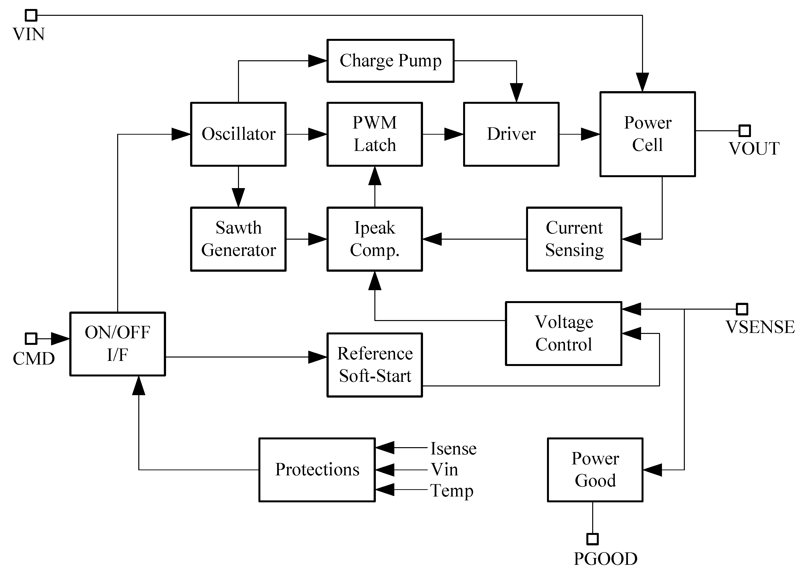
22], but the PoL schematic is reminded in
Figure 1:
PoL is a space qualified product, characterized with the use of component-level tests up to TID level of 50 krad and LET level of 80 MeV·cm
2/mg [
7].
An overview of radiation tests of the PoL performed within this study is given in
Table 2. TID and SEE tests are presented shortly, as well as the mixed-field tests at the CHARM facility.
The next chapters of this paper shall present aggregated, cross-sectional analysis of test results from the seven test campaigns summarized in
Table 2, with a special focus on the opportunities and limitations of the system-level testing.
3. Opportunities Given by System-Level Testing
The primary outcome of the system-level testing of electronics is the characterization (electrical, functional) of the whole system by a single test, i.e., the system-level test may provide:
for TID tests: information on the degradation of observed parameters as a function of TID, information on the TID level that the failure of the system is observed,
for SEE tests: energy/LET threshold of specific system-level or component level effect, a cross section of these effects (as a function of energy or LET),
for mixed-field tests at CHARM: a number of events and information on the degradation due to cumulative effects in the environment defined by the high energy hadrons spectrum.
With these data, the user acquires some level of confidence in the system’s radiation performance in a cost-efficient way. The amount and quality of data collected during system-level test will highly depend on the observability of system parameters provided by the test setup. Information from the system-level test might be used for design validation, or as an input for design improvements. Results have different specificity for TID and SEE test campaigns, therefore these two types of tests will be discussed separately.
3.1. Opportunities Given by TID Tests
Firstly, the opportunities resulting from performing the TID system-level radiation tests will be presented. These observations come from the Co-60 and X-rays irradiations performed on the PoL modules.
3.1.1. Margins Given by the System Are Incorporated in Test Results
One of interests in performing system-level testing is to evaluate margins given by the system. It is expected that the system may withstand a higher TID level than it results from component-level testing performed in the worst case conditions for specific components. This prediction is based on the fact that: (1) typically not all of the components in the system are working in their worst-case conditions, and (2) system designers apply safety margins (derating).
TID irradiations of the PoL allowed to observe these margins: it was observed that although degradation of the oscillator frequency is beyond design limits and beyond level obtained during component-level qualification of the core part of the oscillator, the system remains functional. Furthermore, although the system was qualified up to 50 krad based on Co-60 testing following the classical standard procedures [
7], it could withstand 400 krad at X-ray (high dose rate) and at least 118 krad at Co-60 (low dose rate)—although, the test was not performed in the worst case conditions. Analysis of the results have shown that the extension of the TID tolerance of the system is related to compensations between some electrical blocks in the complete system—a broad description of this example was given in [
22].
In general, it might be expected that system TID performance will be higher (or at least not lower) than the one derived from component-level testing and system-level testing is an interesting tool to estimate this overall performance. On the other hand, there is also a risk of overestimating system TID performance, if system tests are not performed in the worst-case condition—and if this condition will be met in the real use situation.
3.1.2. New Insight into Details of the System’s Radiation Performance
Results of the system-level radiation tests may be the source of valuable information about the system details, and different PoL test campaigns also gave such information.
In the X-rays test (already mentioned in
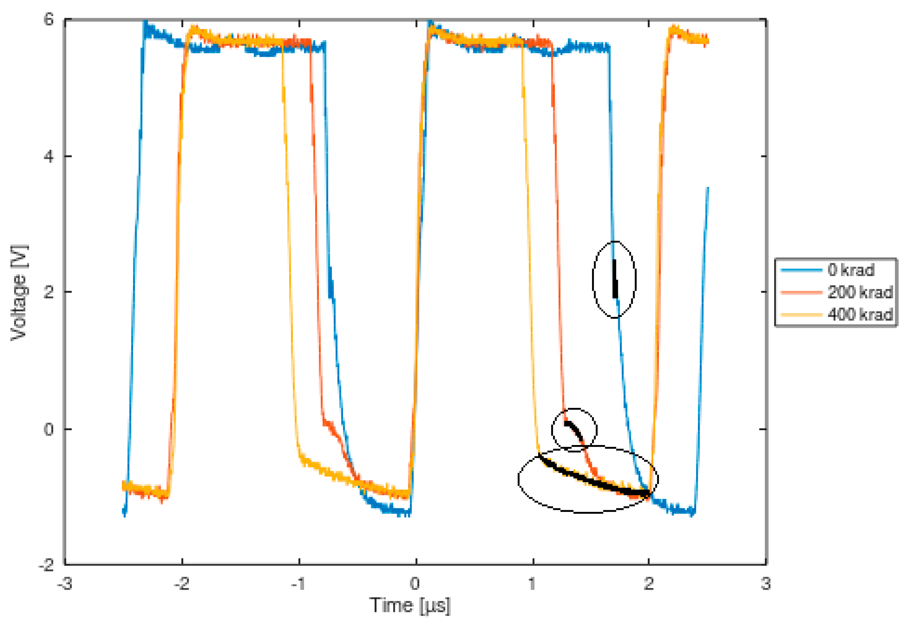
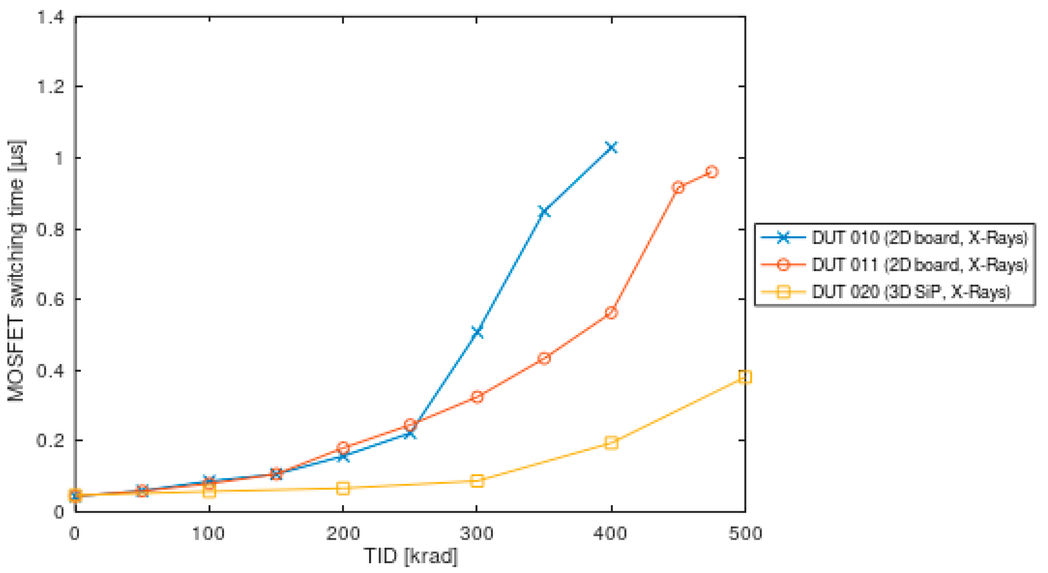
Section 3.1.1) it was possible to reach in relatively short time (around 8–10 h of irradiation) the total dose level high enough that the functional failure of two PoL modules was observed: above 400 krad and above 475 krad irradiation steps. More than 30 different electrical parameters were measured during each irradiation step of the TID tests, giving good observability during this experiment. Thanks to this good observability, it was possible to track the most sensitive component in the system (power MOSFET) and its most critical parameter, the MOSFET switching time (see
Figure 2 for the recording of MOSFET driver waveforms in one of the irradiated PoL 2D boards and
Figure 3 for the degradation of the MOSFET switching time in all three PoL modules irradiated with X-rays).
This test has shown that system-level TID irradiation may be useful to (1) assess which parts should be replaced in the system to extend its radiation performance, (2) evaluate general radiation performance (TID level that the system may survive), (3) to define error signatures for the system. Such TID system-level test might be an interesting tool for verification of mature designs, but also evaluation at the early development phase of product/project.
3.2. Opportunities Given by SEE Tests
In this section, the opportunities resulting from performing the SEE system-level radiation tests will be presented. These observations come from the heavy ions, laser and mixed-field irradiations performed on the PoL modules (see
Table 2 in
Section 2).
3.2.1. Margins Given by the System Are Incorporated in Test Results
Some kind of margins might be also expected in the SEE system-level testing: masking of soft SEEs (such as single event upsets (SEUs) or single event transients (SETs)) or mitigation of some hard SEEs (such as single event latchup (SEL)) by protection mechanisms applied at system-level. Therefore, system-level SEE testing might also give more realistic results than tests at the component level because these masking and mitigation effects will be included in test results.
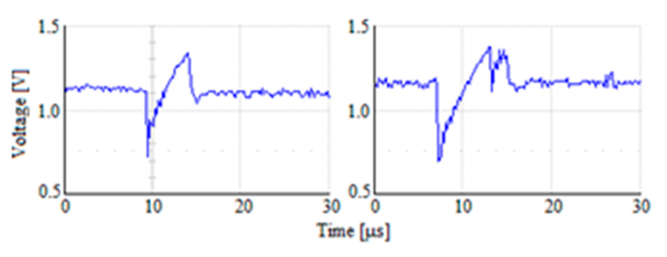
As an example of soft SEE masking, several test campaigns (e.g., heavy ion tests at GANIL, CHARM mixed-field, CHARM heavy ions, heavy ion tests at UCL, laser tests using the IES PRESERVE platform of the University of Montpellier) enabled to observe SETs at the voltage reference chip output, but most of these transients were not propagating to the general output of the device. These SETs were filtered out by the internal filter in the PoL circuit. An example of such a non-propagating transient (one of the several thousand similar events recorded during the CHARM UHE experiment) is presented in
Figure 4 (left curve).
Such results might be used for verification of the mitigation techniques efficiency in the system.
3.2.2. New Insight into Details of the System’s Radiation Performance
Apart from the SET masking, there were also rare events observed during the CHARM UHE experiments, when SETs with the special signature (as on the right curve of
Figure 4) were forcing power cycling of the device. The calculated cross-section for this event is between 1.3·10
−8 and 2.3·10
−8 cm
2, whereas the cross-section for SETs observed at the output of voltage reference chip is in order of ~10
−5 cm
2. Detailed investigation of this phenomenon (presented fully in [
6]) has shown that this specific signature of SETs is most probably due to double hits of ions at sensitive area of the chip, one hit after another shortly in time, therefore it is not something that should be expected in real operation conditions. Furthermore, it could be only observed after the significant degradation of the system due to cumulative effects, which was then leading to an increase of the voltage drop on the supply cables and a decrease of the supply voltage (as measured directly at PoL input). However, observation of such rare events enables to identify new failure modes (system-specific) and therefore to define error signatures for the system.
The presented example of the “rare event” observation shows that the system level testing may also provide information on synergistic effects at the system level: observed propagation of the SET was enabled by system degradation due to cumulative effects. Such effect had not been observed earlier and was very difficult to predict by analysis or component-level testing only. As for today, there is no procedure to evaluate synergistic effects and test at the system level seems to be the only way do to it.
3.3. Opportunities Given by System-Level Testing—Summary
Summarizing this section, it was shown based on different system-level radiation tests, that such tests might be useful in these areas:
to verify the mitigation techniques efficiency,
to identify new failure modes,
to define error signatures for the system,
to assess which parts should be replaced in the system,
to evaluate general TID performance,
to provide information on synergistic effects at the system level.
4. Limiting Factors of Qualification
Although there are interesting opportunities given by the system-level testing, performed experiments let also point out the crucial limitations in terms of system qualification by system-level test only. The most relevant results are presented in this section. Specific remarks for SEE and TID test cases will be given.
4.1. The Worst Case TEST Conditions
For the component-level tests, worst case configuration is well defined and described in standards [
26,
27] and literature [
28,
29]—both in terms of component configuration (such as applied bias) and in terms of environmental conditions (such as temperature or dose rate). In the case of system tests, the definition/choice of the worst-case conditions is more complex and might be the primary issue when considering qualification by only system-level tests.
4.1.1. Example of the Worst Case Test Conditions in TID Tests
As it was presented in the previous section, during system-level TID tests of the PoL it was possible to track the most sensitive component in the system and the most critical parameter, the MOSFET switching time. Analysis performed in [
22] has shown that for the high enough degradation, the MOSFET doesn’t open fully (ON resistance is high), therefore it doesn’t provide enough current to the PoL output. However, this gives some clue that the system worst case might be dependent on the PoL output current configuration, i.e., it might be expected that for the higher output current (lower load resistance) the PoL would fail at a lower TID level because the MOSFET would not be able to give this higher current. On the other hand, it is possible that for the lower output current configuration, the TID failure threshold would be even higher than it was observed during the X-rays experiment.
4.1.2. Example of the Worst Case Test Conditions in SEE Tests
Another example mentioned in
Section 3.2.2 was the SET propagation (during heavy ions test at CHARM), that was leading to power cycling of the PoL device. As it was already explained, this power cycling was only observed when the supply voltage of the PoL was significantly reduced. Then, we may see the dependence of the specific system-level effect from the power supply conditions: reduced supply voltage turns out to be the worst case condition for the propagation of these specific transients. Furthermore, this propagation was only observed for the specific signature of SETs (see
Figure 4), which was produced by two particles passing the sensitive region of the voltage reference chip closely in time. Therefore, a high flux of these particles was needed to produce such an effect, which leads to another conclusion, that not only specific supply configuration, but also specific environmental condition (high particle flux) was needed to produce discussed effect.
4.1.3. General Remarks Regarding the Worst Case Test Conditions
Presented results may lead to the more general conclusions, that each system might have its own, specific worst-case configuration (such as internal state (ON/OFF/idle), input/output voltage, output load, clock frequency, number of system-specific operations per time unit, etc.) that is mostly related to the system internal design and might be difficult to predict without thorough analysis (acquiring more complex for more complex systems). In addition, it might be expected that for some systems only testing in different configurations will show what is the worst-case configuration. For some systems it may be possible to simplify this problem by testing in real conditions only, instead of worst-case conditions, therefore limiting the number of required tests. However, in many cases, e.g., for systems with many internal modes or functions, real conditions cannot be covered by testing in one configuration only.
On the other hand, environmental worst-case conditions might be different for different parts in the system (depending on the component technology), therefore it might be required to irradiate the system in different temperatures or dose rates to meet the worst-case condition for all the components onboard.
For example, when considering temperature, it is confirmed that for TID testing of components, both higher and lower temperatures might be the worst case, depending on the component type. For the SEE testing, the worst case condition for SEL is the high temperature, whereas for Single Event Burnout it is the low temperature. SEU testing is typically performed at room temperature, however, some specific IC designs may show up to have SEU rates dependent on the temperature. [
28] Therefore, it may turn out that for complex designs, including different types of components, SEE testing should be performed over the full temperature range for the system. For TID, it should be sufficient to irradiate the system at one temperature and characterize it in different temperatures. In the example of PoL tests at CHARM mixed-field (see [
24]), it was expected to observe SEL in the PoL with modified components—one of the components was known to be sensitive to SEL at LET as low as 1.2 MeV·cm
2/mg and its anti-latchup protection was removed. However, the latchup characterization of the component was performed at 125 °C and the test at CHARM was at room temperature, therefore not the worst case for SEL—this could be the reason why SEL was not observed during mixed-field tests at CHARM, although the high energy hadron fluence was as high as 3.47·10
11 cm
−2 and the CHARM secondaries typical maximum LET is 15 MeV·cm
2/mg.
4.2. Number of SUT Samples to Test
According to the component-level tests standards (such as ESCC 22900 and ESCC 25100), the number of samples required for qualification tests is 11 samples and 3 samples for TID tests and SEE tests, respectively, if the samples are from the same lot. For TID, it is required to test 5 samples biased, 5 samples unbiased and have one unirradiated control sample [
27]. These recommendations result from the fact that there is always some part-to-part variability of parameters, even for the parts from the same lot, therefore the goal of tests is to obtain a statistical result.
4.2.1. Considerations on Number of SUT Samples in TID Tests
In our TID tests, such part-to-part variability was also observed. Let us take an example of the MOSFET switching time degradation during X-rays tests (see
Figure 3). In all PoL modules that were tested, the MOSFET transistors were from the same production lot. Let us focus on test results for PoL 2D boards: even if the test configuration was the same, there might be observed faster degradation of the SUT010 MOSFET (blue colour) when compared to the SUT011 MOSFET (red colour), This difference is supposed to be the main factor explaining why the system-level degradation, and—finally—functional failure of the SUT010 device is observed at lower TID level than for SUT011. This result shows that the part-to-part variability might be transformed into the SUT-to-SUT variability: TID testing of only one SUT doesn’t give full information about the TID performance of given device series, even if the components in the series are from the corresponding production lots. Testing of a higher number of SUTs is required to give reliable information on the TID radiation performance of the system.
On the other hand, if some risk might be accepted, one of the ways to reduce the required number of SUT samples would be to irradiate this reduced SUT sample set to a much higher TID level than expected in the final application of the system. In [
9] it was chosen to irradiate the system (equipment) to the level 300 times higher than expected in the target application, to accept it for use. Although such margin is typically difficult to achieve for space applications, this approach might be sometimes feasible. If it is possible to irradiate the system up to the catastrophic failure and if it is possible to track the source of failure (such as in an example of X-ray tests [
22]), this information might be also useful for further analysis of the TID level that system may withstand.
4.2.2. Considerations on Number of SUT Samples in SEE Tests
Considering system-level SEE testing, a recommendation from ESCC 22500 to test 3 samples (i.e., system units/instantiations in this case) seem to be appropriate for systems where parts are taken from the same production lots. The effect of each SEE on the system should be considered as independent from other SEEs, therefore such a system-level test might be considered as a simultaneous test of many integrated circuits inside of the system, incorporating part-to-part variability. Therefore, there is no need to perform tests on a higher number of SUT units, even if there is a higher number of integrated circuits in the system.
4.3. Irradiation Source Issues
Typical issues with the irradiation source to be used, are related to the beam penetration and the size of the SUT that might be irradiated with the homogenous beam.
4.3.1. Irradiation Source Issues in TID Tests
For TID tests, the Co-60 standard radiation source has high penetration and usually test area size is also accurate for even big systems. If another source is used, such as X-rays, constraints from the point of view of both penetration and available test area should be taken into account.
4.3.2. Irradiation Source Issues in SEE Tests
Beam parameters such as beam penetration range and beam size may be problematic particularly in SEE tests. Due to limited penetration of, e.g., heavy ions, component packages often need to be opened before irradiation (it was the case for the PoL tests at GANIL and UCL facilities). Sometimes chip dies need to be even thinned to assure that the ions reach the sensitive volume (s). Additional problems may arise when it comes to soldering the fragile component with the opened package on the PCB board. For system-level tests, it happens that it is not possible to irradiate all the components with the same LET value in one run, because components are on different layers of PCB. Furthermore, for systems that are not intended to be opened for testing (such as whole satellites or “black box” systems), penetration of the beam becomes a critical limitation for irradiating with high LET ions. (Considerations on the penetration of heavy ions in board-level tests, as well as related test methodology have been discussed in [
14]). Another limitation comes from the particle beam size: it will be a problem with beam uniformity when irradiating larger components or systems, but for system-level testing, it may turn out to be impossible to irradiate the whole system at once and different parts of the big system shall be irradiated one after another. (See
Table 3 and
Table 4 for the information on beam parameters of the chosen heavy ion and proton facilities.) However, the CHARM facility operating in mixed-field mode allows for the beam uniformity typically bigger than in standard facilities used for SEE testing.
4.4. Observability of Parameters
Observability of system parameters is important for monitoring of events during irradiation and assessment of the system health during or after irradiation. It is also crucial for tracking of failure root cause in the system (as it could be seen in the example of the PoL failing under X-ray: the source of failure could be tracked down to a failure of a single component thanks to high observability of parameters, see [
22]).
One of the limitations in the observability is intrinsic for system-level testing, as it comes from the system integration. We can imagine, e.g., OpAmp being part of the complex circuit—it is not possible (or really hard) to measure OpAmp’s bias current and many other parameters, while it’s embedded in the system. Component-level testing, giving access to all the part’s interfaces, is not restricted in this way and enables characterization of a broader number of parameters. However, limitation in the observability resulting from the system integration is not always the drawback, because not all of the parameters of the components in the system are important for monitoring, and usually, the system designer enables monitoring of the most important parameters by providing dedicated interfaces.
As it was discussed in
Section 4.1, the radiation response of an electronic component may depend on the configuration used, such as supply voltage, operating frequency, etc. When testing at the component level, we are free to use any configuration that we want, because we are irradiating only a single part. When testing at the system level, we are limited to the configurations imposed by the system. It may be only one configuration or range of options to choose from but still limited by the design of the system. From this point of view, observability is reduced again by the system that not only limits access to component interfaces but also imposes specific allowed configurations that components may work—but this type of observability reduction should not limit capabilities of qualifying by system-level test, because there is only loss in observing components’ performance in configurations that would never be used in the system.
4.4.1. Observability of Parameters in TID Tests
There is an advantage of TID tests over SEE tests in terms of observability coming from the fact that it is possible to perform remote testing after TID irradiation: DUT (device under test) or SUT might be removed from the beam area to perform electrical/functional characterization.
4.4.2. Observability of Parameters in SEE Tests
Contrary to TID tests, SEE test measurements need to be performed in-situ. This may lead to significant limitations due to facility mechanical constraints, such as length and/or number and type of available cable connections to monitor electrical and functional parameters (this limitation was met during each SEE test campaign of the PoL, but was particularly cumbersome during test campaigns at CHARM facility, see [
6,
24,
25]).
5. Discussion
Regardless of the different limitations of the system-level testing that were presented in chapter 4, this approach might be still useful in product development. Particularly, let us further discuss the example of SiP modules from 3D PLUS: the company has a database of tests at the device level, so they have knowledge of the device sensitivity to radiation and lot-to-lot variations. They are then able to identify risky devices and build systems with expected initial radiation performance reasonably good. In this context, system-level radiation tests might be used to verify the performance of 3D PLUS products.
Moreover, the electronic circuits are created by the company designers, who are then able to apply their own proprietary mitigations technics. It is essential to take benefit of the test at the system level because they are able to identify the efficiency of the mitigation techniques and to identify what could be improved. As the SiP is a white box for the company designers, they can increase the number of observability points, to have better insight into system details, particularly during the prototype-level (board-level) testing.
Furthermore, at all design phases, it is possible to identify failure modes and error signatures for the system and to evaluate general TID performance. This might be an interesting added value in the design process.
Qualification limitations presented in chapter 4, might be at least partially addressed in the SiP product development flow:
to define the worst case test conditions, testing in different configurations is needed, but the knowledge about the system design may facilitate defining the configurations to verify;
defining the number of SUTs required to have good enough statistical results is important; testing the SiP models at early development phases (e.g., without full mechanical, thermal qualification) might significantly reduce the cost, if it turns out that a high number of SUTs is needed to test;
in terms of beam limitations, which are particularly strong for SEE tests, testing the SiP at 2D board level (instead of the 3D module) would usually increase the value of performed tests, because the beam penetration might be lower, therefore the available LET range of particles increases;
in terms of the system observability, limitations are again stronger for SEE tests, but here the solution could be the use of the supplementary instrumentation in digital SUTs [
31] to increase the observability (for the cost of additional development).
Nevertheless, the complete system qualification, i.e., the one that would overcome all the qualification limitations discussed in chapter 4, is difficult. Furthermore, the cost of performing such complete qualification might be too high to make it a useful tool for the product or mission development. In some cases, simplification of the qualification is possible thanks to the knowledge about the system design or thanks to the knowledge about the target environment. However, for most of the cases, complete system qualification by system-level test remains difficult, and it is justified to consider the development of the limited qualification approach, that might be easier to apply, give valuable information, while bringing some level of risk that needs to be accepted.
Limited qualification scenarios and risk acceptance should be considered in the context of the system reliability and availability. High reliability space missions require maximum reliability (the system is not destroyed and is working within the specifications) and availability close to 100% (availability defined as a percentage of time that the system can be used during the mission, this percentage might be decreased by, e.g., power cycling of the system due to SEFI (single event functional interrupt)). High reliability missions will never accept qualification scenarios that introduce some risk in the reliability and will rarely accept any risk in the availability, even if the effort of the qualification will be lower.
On the other hand, for New Space missions, controllable risk acceptance is one of the fields to look for savings. Lower system availability, if justified, might be acceptable. Even slightly reduced system reliability might be considered if the system is understood as a single satellite in the constellation, where the mission (constellation) success is possible with partial loss of satellites. This opens the doors for use of limited TID/SEE qualification scenarios for the final qualification in New Space applications.
6. Conclusions
Based on the experimental results from several radiation test campaigns, the overview of opportunities and limitations of system qualification using the system-level radiation testing was presented. Impact on the SiP product development was discussed. Limitations for the SEE qualification are substantially stronger than for the TID qualification, however, there are still important question marks regarding also TID qualification: how to define the worst case conditions, how important is testing in these conditions, how many system units should be tested to have a high confidence level of results? Future works are planned to answer some of these questions, as well as to investigate the limited qualification approach for system qualification.
Author Contributions
Conceptualization, T.R., F.S. and P.-X.W.; methodology, T.R., F.S. and P.-X.W.; software, T.R.; validation, T.R., F.S. and P.-X.W.; formal analysis, T.R. and F.S.; investigation, T.R., F.S. and P.-X.W.; resources, T.R., F.S. and P.-X.W.; data curation, T.R.; writing—original draft preparation, T.R. and F.S.; writing—review and editing, T.R., F.S. and P.-X.W.; visualization, T.R.; supervision, F.S. and P.-X.W.; project administration, F.S. and P.-X.W.; funding acquisition, F.S. and P.-X.W. All authors have read and agreed to the published version of the manuscript.
Funding
Laser: X-rays and Co60 tests have been performed using the PRESERVE Platform which has been funded by the Occitanie Region and the EU via ERDF funds. This work has received funding from the European Union’s Horizon 2020 research and innovation program under the Marie Skłodowska-Curie grant agreement number 721624.
Institutional Review Board Statement
Not applicable.
Informed Consent Statement
Not applicable.
Data Availability Statement
Most of data used for this study might be found at [
6,
22,
23,
24,
25].
Acknowledgments
This work was realized within the RADSAGA project. The RADSAGA Innovative Training Network project has received funding from the European Union’s Horizon 2020 research and innovation program under the Marie-Skłodowska-Curie grant agreement number 721624. Authors wish to thank colleagues from CERN for their support in organizing and performing tests at the CHARM facility: Rubén García Alía, Salvatore Danzeca, Chiara Cangialosi, Pablo Fernández-Martínez, Maria Kastriotou, Andrea Coronetti, Nourdine Kerboub and Corinna Martinella.
Conflicts of Interest
The authors declare no conflict of interest. The funders had no role in the design of the study; in the collection, analyses, or interpretation of data; in the writing of the manuscript, or in the decision to publish the results.
References
- Mangeret, R. Radiation hardness assurance: How well assured do we need to be? In Proceedings of the 2018 IEEE NSREC Conference Short Course Notebook, Kona, HI, USA, 16–20 July 2018. [Google Scholar]
- Campola, M.; Pellish, J. Radiation Hardness Assurance: Evolving for NewSpace. In Proceedings of the 2019 RADECS Short Course Notebook, Montpellier, France, 16–20 September 2019. [Google Scholar]
- Perez, F. Overview of ESA CubeSat Missions and Radiation Testing on CubeSat Electronics. In Proceedings of the 2021 RADECS Conference Short Course Notebook, Vienna, Austria, 13 September 2021. [Google Scholar]
- Coronetti, A.; Alía, R.G.; Budroweit, J.; Rajkowski, T.; Da Costa Lopes, I.; Niskanen, K.; Söderström, D.; Cazzaniga, C.; Ferraro, R.; Danzeca, S.; et al. Radiation hardness assurance through system-level testing: Risk acceptance, facility requirements, test methodology and data exploitation. IEEE Trans. Nuclear Sci. 2021, 68, 958–969. [Google Scholar] [CrossRef]
- Hi-Rel Point-of-Load DC/DC Converter. 3D PLUS Product Datasheet, 3DFP-0296-REV. 6 April 2017.
- Rajkowski, T.; Saigné, F.; Pouget, V.; Wrobel, F.; Touboul, A.; Boch, J.; Kohler, P.; Dubus, P.; Wang, P.X. Analysis of SET Propagation in a System in Package Point of Load Converter. IEEE Trans. Nuclear Sci. 2020, 67, 1494–1502. [Google Scholar] [CrossRef]
- Vassal, M.-C.; Dubus, P.; Fiant, N. Electrical performances and radiation qualification tests results of a highly integrated and Space qualified Point of Load Converter. In Proceedings of the 12th European Conference on Radiation and Its Effects on Components and Systems, Sevilla, Spain, 19–23 September 2011. [Google Scholar]
- Rousselet, M.; Adell, P.C.; Sheldon, D.J.; Boch, J.; Schone, H.; Saigné, F. Use and benefits of COTS board level testing for radiation hardness assurance. In Proceedings of the RADECS 2016, Bremen, Germany, 19–23 September 2016. [Google Scholar]
- Fernández, G.; Bárcena, J.; Muñoz, E. TID test on ITER Interlock Discharge Loop Interface Box (DLIB) system, an example of radiation test at equipment level. In Proceedings of the RADECS 2017, Geneva, Switzerland, 2–6 October 2017. [Google Scholar]
- Virmontois, C.; Belloir, J.; Beaumel, M.; Vriet, A.; Perrot, N.; Sellier, C.; Bezine, J.; Gambart, D.; Blain, D.; Garcia-Sanchez, E.; et al. Dose and Single-Event Effects on a Color CMOS Camera for Space Exploration. IEEE Trans. Nuclear Sci. 2019, 66, 104–110. [Google Scholar] [CrossRef]
- O’Neill, P.M.; Badhwar, G.D.; Culpepper, W.X. Risk assessment for heavy ions of parts tested with protons. IEEE Trans. Nuclear Sci. 1997, 44, 2311–2314. [Google Scholar] [CrossRef] [PubMed] [Green Version]
- Guertin, S. Board Level Proton Testing Book of Knowledge for NASA Electronic Parts and Packaging Program; NASA JPL Publication: Pasadena, CA, USA, 2017. [Google Scholar]
- Guertin, S. Lessons and Recommendations for Board-Level Testing with Proton; Small Satellite Conference: Logan, UT, USA, 2018. [Google Scholar]
- De Bibikoff, A.; Lamberbourg, P. Method for System-level testing of COTS electronic board under High Energy Heavy Ions. IEEE Trans. Nuclear Sci. 2020, 67, 2179–2187. [Google Scholar] [CrossRef]
- Alía, R.G.; Martínez, P.F.; Kastriotou, M.; Brugger, M.; Bernhard, J.; Cecchetto, M.; Cerutti, F.; Charitonidis, N.; Danzeca, S.; Gatignon, L.; et al. Ultraenergetic heavy-ion beams in the CERN accelerator complex for radiation effects testing. IEEE Trans. Nuclear Sci. 2019, 66, 458–465. [Google Scholar] [CrossRef] [Green Version]
- Fernández-Martínez, P.; Alía, R.G.; Cecchetto, M.; Kastriotou, M.; Kerboub, N.; Tali, M.; Wyrwoll, V.; Brugger, M.; Cangialosi, C.; Cerutti, F.; et al. SEE tests with ultra energetic Xe ion beam in the CHARM facility at CERN. IEEE Trans. Nuclear Sci. 2019, 66, 1523–1531. [Google Scholar] [CrossRef]
- Mekki, J.; Brugger, M.; Alia, R.G.; Thornton, A.; Mota, N.C.D.S.; Danzeca, S. CHARM: A Mixed Field Facility at CERN for Radiation Tests in Ground, Atmospheric, Space and Accelerator Representative Environments. IEEE Trans. Nuclear Sci. 2016, 63, 2106–2114. [Google Scholar] [CrossRef]
- Thornton, A. CHARM Facility Test Area Radiation Field Description. Available online: http://cds.cern.ch/record/2149417 (accessed on 14 January 2022).
- Secondo, R.; Alia, R.G.; Peronnard, P.; Brugger, M.; Masi, A. System level radiation characterization of a 1U CubeSat based on CERN radiation monitoring technology. IEEE Trans. Nuclear Sci. 2018, 65, 1694–1699. [Google Scholar] [CrossRef]
- Coronetti, A.; Manni, F.; Mekki, J. Mixed-field radiation qualification of a COTS space on-board computer along with its CMOS camera payload. In Proceedings of the RADECS 2019, Montpellier, France, 16–20 September 2019. [Google Scholar]
- RADSAGA System-Level Testing Guideline for Space Systems. RADSAGA 2020. Available online: https://edms.cern.ch/document/2423146/2.1 (accessed on 14 January 2022).
- Rajkowski, T.; Saigné, F.; Niskanen, K.; Boch, J.; Maraine, T.; Kohler, P.; Dubus, P.; Touboul, A.; Wang, P.-X. Comparison of the Total Ionizing Dose Sensitivity of a System in Package Point of Load Converter Using Both Component- and System-Level Test Approaches. Electronics 2021, 10, 1235. [Google Scholar] [CrossRef]
- RADSAGA Test Report No. 01: GANIL RADSAGA Campaign, Date: 15/01/2019, Version no. 2.1—EDMS 2086126/1, RADSAGA 2019. Available online: https://radsaga.web.cern.ch/test-reports (accessed on 12 January 2022).
- RADSAGA Test Report No. 02: CHARM RADSAGA Campaign #1, Date: 23/01/2019, Version no. 2.1—EDMS 2086128/1, RADSAGA 2019. Available online: https://radsaga.web.cern.ch/test-reports (accessed on 12 January 2022).
- RADSAGA Test Report No. 05: CERN Heavy Ions RADSAGA Campaign, Date: 27/08/2019, Version no. 1.1—EDMS 2215703 v.1, RADSAGA 2019. Available online: https://radsaga.web.cern.ch/test-reports (accessed on 12 January 2022).
- Single Event Effects Test Method and Guidelines. ESCC Basic Specification No. 25100, Issue 2, October 2014. Available online: http://escies.org/escc-specs/published/25100.pdf (accessed on 20 January 2022).
- Total Dose Steady-State Irradiation Test Method. ESCC Basic Specification No. 22900, Issue 5, June 2016. Available online: http://escies.org/escc-specs/published/22900.pdf (accessed on 20 January 2022).
- Schwank, J.R.; Shaneyfelt, M.R.; Dodd, P.E. Radiation Hardness Assurance Testing of Microelectronic Devices and Integrated Circuits: Radiation Environments, Physical Mechanisms, and Foundations for Hardness Assurance. IEEE Trans. Nuclear Sci. 2013, 60, 2074–2100. [Google Scholar] [CrossRef]
- Schwank, J.R.; Shaneyfelt, M.R.; Dodd, P.E. Radiation Hardness Assurance Testing of Microelectronic Devices and Integrated Circuits: Test Guideline for Proton and Heavy Ion Single-Event Effects. IEEE Trans. Nuclear Sci. 2013, 60, 2101–2118. [Google Scholar] [CrossRef]
- Söderström, D. Board and system level testing in other RADSAGA facilities and beyond. presentation during RADSAGA System Level Test Review, CERN, Geneva, Switzerland, 11–13 November 2019; Available online: https://indico.cern.ch/event/843292/contributions/3541581/ (accessed on 20 January 2022).
- Lopes, I.C.; Pouget, V.; Wrobel, F.; Saigne, F.; Touboul, A.; Røed, K. Development and evaluation of a flexible instrumentation layer for system-level testing of radiation effects. In Proceedings of the 2020 IEEE Latin-American Test Symposium (LATS), Maceio, Brazil, 30 March–2 April 2020. [Google Scholar]
| Publisher’s Note: MDPI stays neutral with regard to jurisdictional claims in published maps and institutional affiliations. |
© 2022 by the authors. Licensee MDPI, Basel, Switzerland. This article is an open access article distributed under the terms and conditions of the Creative Commons Attribution (CC BY) license (https://creativecommons.org/licenses/by/4.0/).


