Article

Theoretical and Experimental Substractions of Device Temperature Determination Utilizing I-V Characterization Applied on AlGaN/GaN HEMT

by
Martin Florovič
1,*,
Jaroslav Kováč, Jr.
1,
Aleš Chvála
1,
Jaroslav Kováč
1,
Jean-Claude Jacquet
2 and
Sylvain Laurent Delage
2
1
Faculty of Electrical Engineering and Information Technology, Slovak University of Technology, Ilkovicova 3, 812 19 Bratislava, Slovakia
2
III-V Lab, Route de Nozay, 91460 Marcoussis, France
*
Author to whom correspondence should be addressed.
Electronics 2021, 10(22), 2738; https://doi.org/10.3390/electronics10222738
Submission received: 14 October 2021 / Revised: 3 November 2021 / Accepted: 4 November 2021 / Published: 10 November 2021
(This article belongs to the Section Microelectronics)

Abstract

:
A differential analysis of electrical attributes, including the temperature profile and trapping phenomena is introduced using a device analytical spatial electrical model. The resultant current difference caused by the applied voltage variation is divided into isothermal and thermal sections, corresponding to the instantaneous time- or temperature-dependent change. The average temperature relevance is explained in the theoretical section with respect to the thermal profile and major parameters of the device at the operating point. An ambient temperature variation method has been used to determine device average temperature under quasi-static state and pulse operation, was compared with respect to the threshold voltage shift of a high-electron-mobility transistor (HEMT). The experimental sections presents theoretical subtractions of average channel temperature determination including trapping phenomena adapted for the AlGaN/GaN HEMT. The theoretical results found using the analytical model, allow for the consolidation of specific methodologies for further research to determine the device temperature based on spatially distributed and averaged parameters.

1. Introduction

The commercial wireless market requires more demanding microwave operation with higher requirements in terms of self-heating, high operating voltage and inherent processes and their impact on the device reliability in consumer electronics [1,2,3]. The presence of two-dimensional electron gas (2DEG) in a gallium nitride (GaN) based structure presents the potential to fabricate high electron mobility transistors (HEMTs) with Schottky diodes employed as excellent devices for application in the microwave and power conversion field. The suppression of the critical temperature increase, caused by high power density along the device active area, requires the utilization of high thermal conductance substrates e.g., silicon carbide (SiC) [4]. Since the devices are microscopic in size, the conventional methods lack the accuracy to estimate the device operating temperature.
Numerous experimental methods were developed to determine the temperature inside and nearby active device area such as Raman spectroscopy or interferometric mapping [5,6,7]. Additionally, various methods utilizing external heating, or a low-power operating regime were employed, taking advantage of specific electro-thermal device properties. However, these methods, that are widely applied to determine average temperature of HEMT operating in the saturation regime, suffer from a lack of accuracy due to the marginalization of the drain current increase caused by, e.g., gate length modulation or leakage effects [8,9,10]. Moreover, the current comparison at the defined operating point to the peak current under short-pulsed operation at various ambient temperatures [11] in these devices does not account for time dependent isothermal phenomena caused processes such as by charge trapping.
Although device thermal simulations, based on non-linear equations, resolve thermal processes inside the structure [12], the combined integral and differential analysis of the resultant current and the separation of the isothermal and thermal sections are emphasized in this work. The complex theoretical considerations, utilizing thermal profile variation, were simplified and adapted for the practical purposes to acquire the average HEMT channel temperature. The theoretical and experimental results obtained are present the potential to improve and consolidate the already utilized methodologies described empirically for specific devices.

2. Theory

2.1. Electrical Model

The presented model is possible to be applied to an n-port device with applied voltage Vn considering resultant current I at one port and neglecting the other port current. Devices meeting these requirements are e.g., Schottky diode, ungated or gated transmission line model (TLM) structure such as field-effect transistor (FET) when neglecting the gate current.
The resultant current change dI (∆I) consists of an isothermal section dIE (∆IE) induced by applied voltage change dVn (∆Vn) and isothermal trapped charge variation dQTE(X) (∆QTE(X)) and thermal section dIT (∆IT) assigned to spatial temperature change dT(X) (∆T(X)) and the thermal trapped charge variation dQTT(X) (∆QTT(X)):
d I = d I E + d I T
The current change is defined for the time interval dt (∆t) considering the device area consisting of spatial elements dX (∆X) and thermal profile T(X). The resultant trapped charge dQT (X) (∆QT (X)) is defined in a similar way, as follows:
d Q T ( X ) = d Q T E ( X ) + d Q T T ( X )
In general, dIE is related to dVn and dQTE(X) by time invariant coefficients kVn and kQ(X), respectively, whereas dIT is related to dT(X) and dQTT(X) by time invariant coefficients kT(X) and kQ(X), respectively:
d I E = k V n d V n + X k Q ( X ) d Q T E ( X ) d X
d I T = X [ k T ( X ) + k Q ( X ) k T T ( X ) ] d T ( X ) d X
In (4) k T T ( X ) = d Q T T ( X ) / d T ( X ) is time and state dependent variable. The coefficients kQ(X), kT(X), kTT(X) and kVn at the operating point defined by Vn, I and T(X) at time t can be obtained using an analytical solution or advanced simulation software calibrated by experimental results. Although the majority of commercially utilized simulation software allows for self-heating to be switched off/on [12] or DC measurements to be realized in a pulse or quasi-static state [13], it is impossible to turn self-heating on separately to obtain T(X) and I at a predefined operating point and to subsequently turn it off for ∆t and ∆Vn to separate ΔIT and ΔIE.
It is recommended that the device current response of a stepping and rectangular pulse source is differentiated into time elements Δt to find the particular ΔIE and ΔIT as shown in Figure 1a,b, respectively. The small parasitic capacitance, typical for GaN-based devices, and a short switching time of the stepping source in comparison with thermal and trapping time constants make it possible for ∆IT to be obtained as the difference between I acquired at t1t and at t1t in the case of a negligible ΔQTE(X). To reach an equilibrium state during quasi-static stepping, the voltage source measurements shown in Figure 1a, Δt is utilized much higher than the thermal and trapping time constants. For the pulse voltage source measurements initialized at time t0 depicted in Figure 1b, the temperature T(X)T0 is found along the active device area at t t 1 , that it is zero ΔVn at t > t 1 and a negligible ΔQTE(X) results in ΔIT ≈ ΔI. Otherwise, ΔQTE(X) is required to be incorporated into ΔIE as illustrated below.

2.2. Average Temperature Definition

To avoid thermal gradient calculations, the average temperature contribution dTA in the active device area XA is defined by the substitution of k T I ( X ) = k T ( X ) + k Q ( X ) k T T ( X ) and the spatially independent thermal coefficient kT related to the operating point:
d I T = k T ( T A , V n ,   t ) d T A = X A k T I ( X ) d T ( X ) d X
To eliminate the k T I ( X ) spatial determination, the approximation, demonstrated by an infinite thermal conductance for which the power density of XA does not perform a function, is usually utilized to calculate average temperature TA with trapping centers thermally excited by the same dTA. Therefore the k T = X A k T I ( X ) d X as TA, Vn and t dependent are used in the following way:
d I T = k T ( T A , V n ,   t ) d T A = [ X A k T I ( X ) d X ] d T A
The deviation between (5) and (6) leads to a discrepancy in TA determination, especially for different heat flux distributions caused by power dissipation, ambient temperature and time variation. For a spatially independent kT(X), kQ(X) or kTT(X) in XA, (5) and (6) appear identical, resulting in k T = k T I ( X ) X A and subsequently dTA as the thermodynamic average temperature contribution in XA:
d T A = X A 1 X A d T ( X ) d X

2.3. Ambient Temperature Variation

The average temperature determination method depicted in Figure 2a is based on the resultant current I comparison with an isothermal device current IE at time t1 after the measurement initialization at time t0, where the maximum I and IE should be reached at time t0’. The trapping effects must be included in IE as illustrated below. In spite of the zero thermal contribution X k T I ( X ) d T E ( X ) d X to IE, the variation of the isothermal temperature profile TE(X), together with a spatially dependent k T I ( X ) , results in a thermodynamic average temperature deviation from the initial temperature at t0, caused by the difference between (5) and (6). Therefore, this method is found to be sufficient for devices with a relatively small active area or negligible spatial k T I ( X ) variation.
Two identical measurements at distinct ambient temperatures, such that T01T0 and T02T0 + ΔT* with a small temperature difference ΔT* result in the current I1 and I2, temperature profiles T1(X) and T2(X), as depicted in Figure 2b, and exhibit the temperature profile difference Δ T * ( X ) = T 2 ( X , t 1 ) T 1 ( X , t 1 ) T 2 ( X , t 1 + Δ t ) T 1 ( X , t 1 + Δ t ) , Δ T ( X ) = T 1 ( X , t 1 + Δ t ) T 1 ( X , t 1 ) and the differential current Δ I = I 1 ( t 1 + Δ t ) I 1 ( t 1 ) , Δ I * = I 2 ( t 1 ) I 1 ( t 1 ) I 2 ( t 1 + Δ t ) I 1 ( t 1 + Δ t ) . The assumption of a low Δt means that the following formula is applicable for quasi-static and pulsed operations:
Δ I * = X k T I ( X ) Δ T * ( X ) d X
The substitution of Δ T * ( X ) = Δ T ( X ) Δ T E ( X ) and Δ T E ( X ) = T 1 ( X , t 1 + Δ t ) T 2 ( X , t 1 ) in (8), utilized for the dIT comparison with Δ I T = X k T I ( X ) Δ T ( X ) d X based on the comparison of difference and differential substitution d I T / Δ I T = d T ( X ) / Δ T ( X ) , results in:
d I T Δ I * = X k T I ( X ) d T ( X ) d X X k T I ( X ) Δ T * ( X ) d X
As a result, a TA definition utilizing (6) and substitution XXA, dIT and ΔI* caused by ΔVn and ΔT0 leading to dTA and ∆TA*, respectively, leads (9) to the following relationship:
d I T / Δ I * = d T A / Δ T A *
However, despite the zero IE thermal current, a non-zero ∆TE(X) variation results in a discrepancy between the definition of dTA and ∆TA* by (7) and the definition utilizing infinite thermal conductance of the device active area, on the other side. Nevertheless, the TA determination methods utilizing (10) are found to be sufficient for devices with a negligible spatial k T I ( X ) variation or a relatively small active area.
Already known ∆TA* and ΔIE time dependence allows to obtain TA as the sum of dTA calculated in (10) in the quasi-static or pulsed operating regime. Temperature dependent thermal resistance and thermal capacity result in a ∆TA* deviation from ΔT0. Quasi-static state methods, utilizing the T0 variation, allows for the calculation of dTA and ∆TA* [9,14].

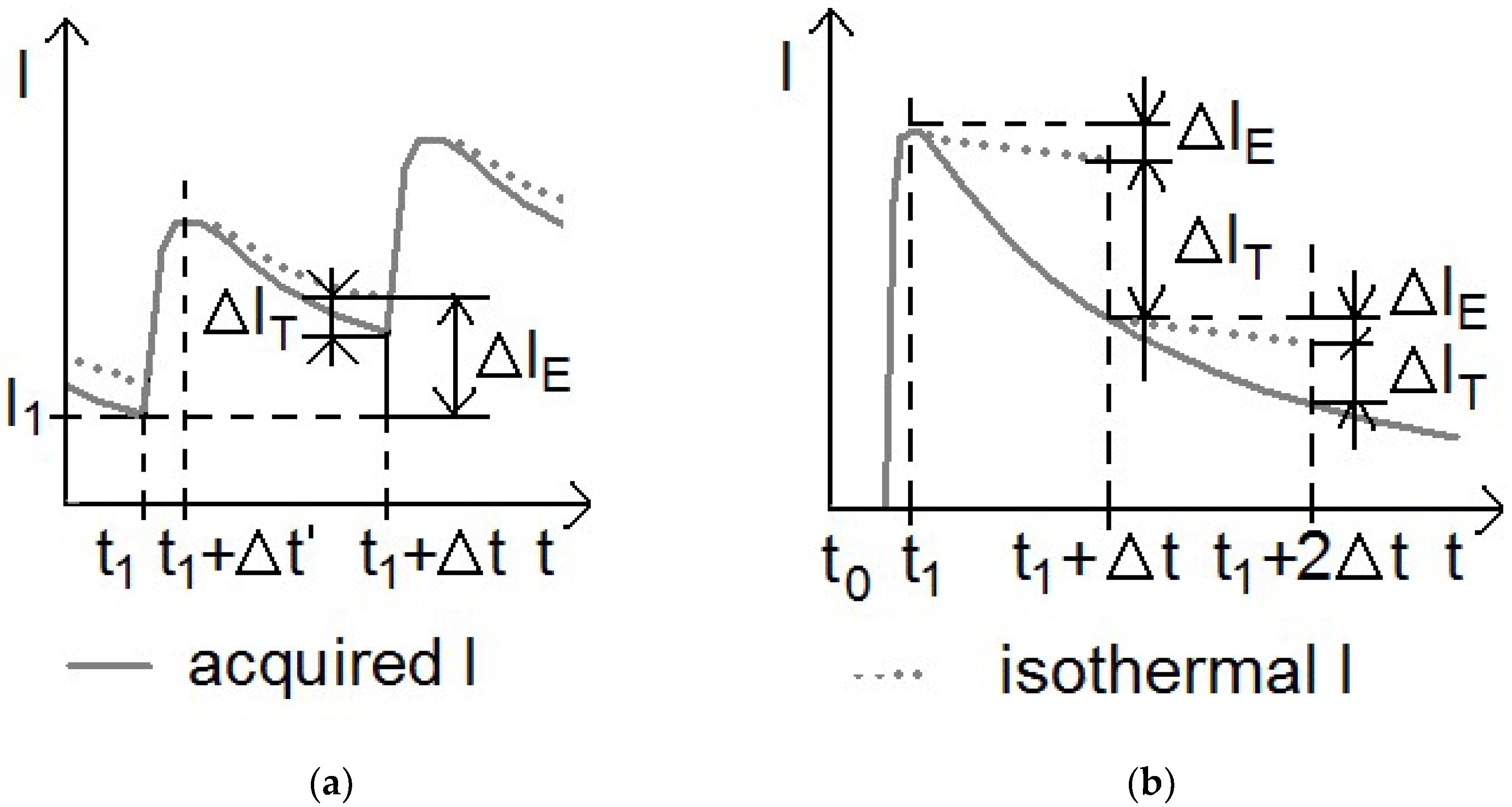
2.4. Trapping Effects Approximation in FET

We further consider the TA determination of the FET-neglecting parasitic gate, and its entire electric capacitance. Even a relative carrier velocity v change, and pinch-off area formation are thought to have no impact on channel potential distribution along the channel [15,16].
The threshold voltage VTH shift is related to the time and temperature variation of energy barrier height, free charge concentration along the conductive channel as well as charge trapping, resulting in the additional virtual gate electrode. The gate voltage VGS, drain voltage VDS and ambient temperature T0 variation causes dTA, with a direct impact on the v and VTH change. These variations result from the isothermal section dVTHN, caused by an immediate band energy diagram and free charge concentration change. The isothermal section dVTHE, is a result of the trapping phenomena during the defined time and the thermal section dVTHT originates from thermal carrier and trap center density change.
A widely utilized FET approximation [15] in the case of stepping VDS and/or VGS at a defined T0 is as follows:
d I = g M 0 ( d V G S d V T H E d V T H T ) + g D 0 d V D S + d I T V
It is possible to acquire the isothermal transconductance gM0 and output conductance gD0 via immediate isothermal VDS and VGS responses, including d V T H N / d V D S and d V T H N / d V G S . The term dITV represents the thermal change caused by dVDS, dVGS and dT0 and has a major impact on v, excluding dVTH. A substitution of d I 0 = g M 0 d V G S + g D 0 d V D S and d I = d I E + d I T , as applied in (11), results in:
d I E = d I 0 g M 0 d V T H E
d I T = d I d I E = d I T V g M 0 d V T H T
A common way to obtain VTH is pulsed and/or quasi-static transfer I-V characteristics utilization at defined T0 and VDS assuming VTH independent on VGS as well as an approximation of isothermal and measured I-V characteristics pointing on the same VTH shift at T0 in the operating range. Trapping phenomena and voltage drop in the source-to-gate and drain-to-source area have a partial influence on the VTH determination especially for low applied VDS or non-linear VTH vs. VDS dependence. The following ways of trapping effects incorporation in TA calculation coming out of VTH determination from transfer I-V characteristics are explained.
In the case of the quasi-static state operation VTH shift, resulting in ( d V T H E + d V T H N ) / d V D S caused by T0 and VDS variation, can be simply obtained from quasi-static I-V characteristics. Transfer I-V characteristics, measured by short-pulsed VGS and VDS offering trap influence separation, allow to get d V T H N / d V D S obtained from negative VTH shift caused by roll-off effect in short-channel FET [15,17]. Subsequently, the ratio d V T H E / d V D S dependent on VDS and T0 is acquired and utilized in (12), whereby dI0 is acquired at the beginning of VDS and/or VGS step, a measured transconductance g M | g M g M 0 | is supposed. For a significant g M d V T H E / d V D S temperature variation in comparison with d I T / d V D S an iteration process is required for TA determination.
For VDS and/or VGS pulse responses, depicted in Figure 1b, the pulsed transfer I-V characteristics are measured utilizing VGS and/or VDS quiescent biasing and/or voltage pulses. At T0 and the defined time t1 after the increase of constant amplitude VDS and the sweeping amplitude VGS, drain currents are acquired to extract the VTH as t1 and T0 functions. At the time interval ∆t, during the pulse, Δ V T H E = V T H ( T A ,   t 1 + Δ t ) V T H ( T A ,   t 1 ) gives the opportunity to utilize Δ I E = g M 0 Δ V T H E for both a small Δt and ΔVTHE corresponding to the virtual gate electrode potential shift, neglecting the gM0 time variation. The maximum resultant current IE and VTH, obtained immediately after VGS and/or VDS rising edges at t0, provides the opportunity to plot the IE time dependence at T0, depicted in Figure 2a:
I E ( t 1 ) = I E ( t 0 ) g M 0 [ V T H ( t 1 ) V T H ( t 0 ) ]
In the considerations above a thermal gradient along the active device area that effects the trap spatial localization is truncated. Isothermal trapping phenomena and a voltage drop in the source-to-gate and the drain-to-source area having a partial influence on VTH shift are neglected as well. Despite this, an appropriate analytical approximation of the I-V characteristics provides an opportunity to predict the trapping phenomena in particular devices. An advantage of the T0 variation method during the device operation is that the calibration of for d I T V / d T A vs. TA, VDS and VGS with an additional trapping phenomena analysis is not required.

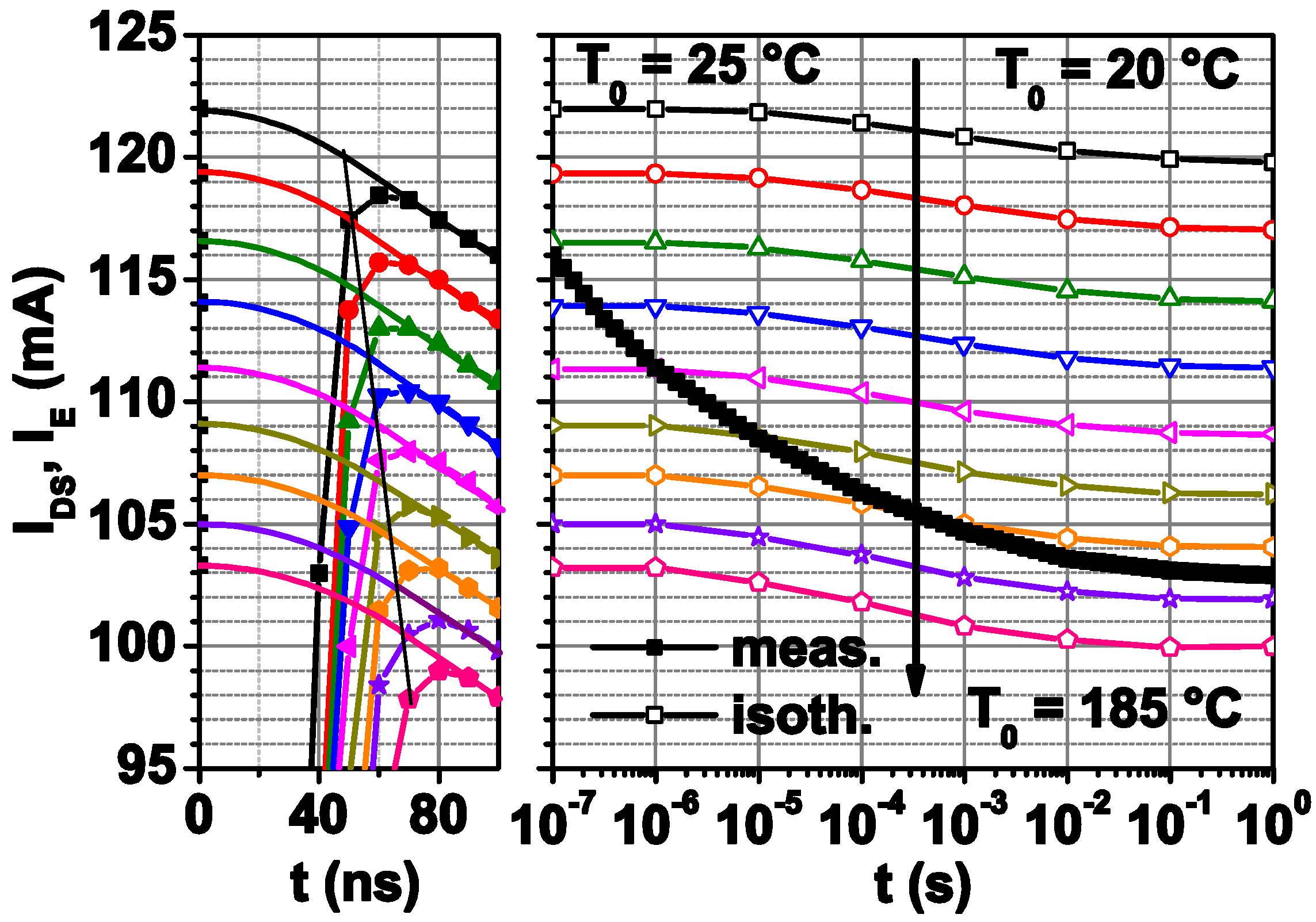
2.5. Short Time Response Current Utilization

Many of the experimental methods that are widely utilized for the TA acquisition of FET in a saturation regime are based on a zero isothermal drain current change d I E / d V D S at constant VGS. The requirement of zero dIE in (12) is satisfied for a gate length modulation or a leakage current increase compensated by the trapping phenomena in the saturation regime, resulting in d I E d I T . Long-channel FET excluding VDS such as VGS dependent charge trapping variation meets this condition therefore the methods to acquire TA in quasi-static operation coming out from temperature calibration of major electrical parameters [8,16] or ambient temperature variation [9,18] require standard DC measuring equipment. The dIE prediction at various ambient temperatures, using an analytical model or simulation software also makes such methods applicable for short-channel FET [17,18].
In general, the resultant current acquisition after a short period after the voltage step/pulse is required, to obtain the dI0. The method depicted in Figure 2a is simply applicable for devices exhibiting relatively short time responses t0t0, operating in the quasi-static and dynamic state as well providing the opportunity to obtain an isothermal trapping effects approximation. However a switching time of ~10−8 s is required for full load turning-on, which makes the experimental setup more expensive.

3. Experimental

3.1. Structure Design and Experimental Setup

The investigated Al0.25Ga0.75N/GaN HEMT structure, including 14 nm Al0.25Ga0.75N/1.5 nm AlN/1700 nm GaN/75 nm thermal boundary resistance layer (TBR) heterostructure was grown by MOVPE on a 70 μm thick 4H-SiC substrate, containing the backside Au contact, which was soldered to 1 mm thick CuMo leadframe using a 60 μm thick AuSn solder. The top ohmic drain/source and gate contacts were created via standard Au-based metallization. A gated transmission line model (GTLM) HEMT with a width of w ≈ 100 μm, a gate with a length of dG ≈ 0.15 μm, asource to gate gap of length dGS ≈ 0.75 μm and the drain to gate gap of length dGS ≈ 1.5 μm was investigated [14]. The device is placed in an open package located on the Al thermal chuck and maintainedat a constant temperature.
A semiconductor parameter analyzer Agilent 4155C and controlled thermal chuck were utilized to acquire the output characteristics at zero gate-source voltage VGS and the drain-source voltage VDS varied from 0 V up to 20 V. The chuck temperature was set in the range of 25–185 °C to demonstrate methods based on ambient temperature and threshold voltage variation. The device trapping level was reset via white LED illumination for one minute between quasi-static measurements. The 3D model incorporating device geometry, layout and thicknesses of individual layers was created using the 3D thermal FEM simulations performed by Synopsys TCAD Sentaurus [12]. The material thermal conductivity and capacity values were obtained from the previous work and calibrated utilizing the measurements provided [19,20]. The constant ambient temperature boundary condition was set to the structure backside, assuming an ideal heat transfer between leadframe and heatsink. The structure’s self-heating is simulated by three thermal contacts placed along 2DEG, between the drain and source, representing heat contribution from the drain to the source access region, under the gate electrode and the pinch-off region located at the drain side gate edge [19].

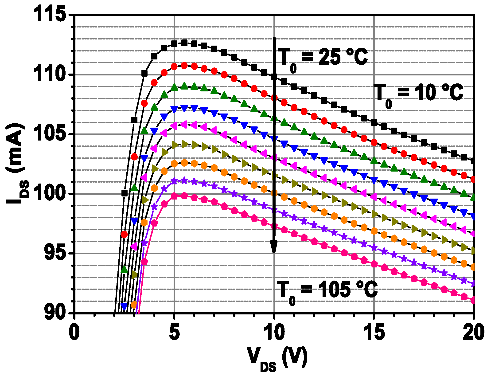
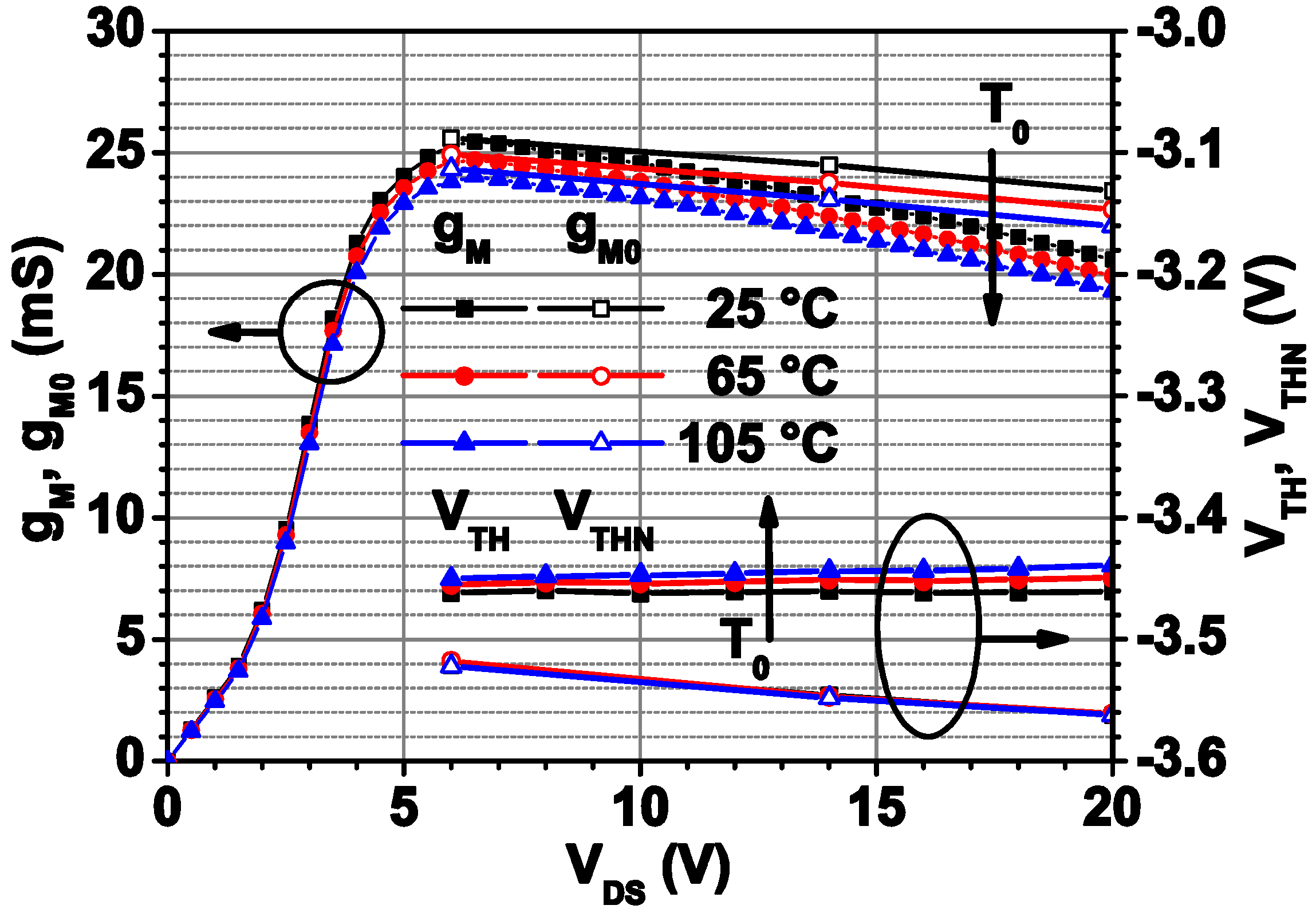
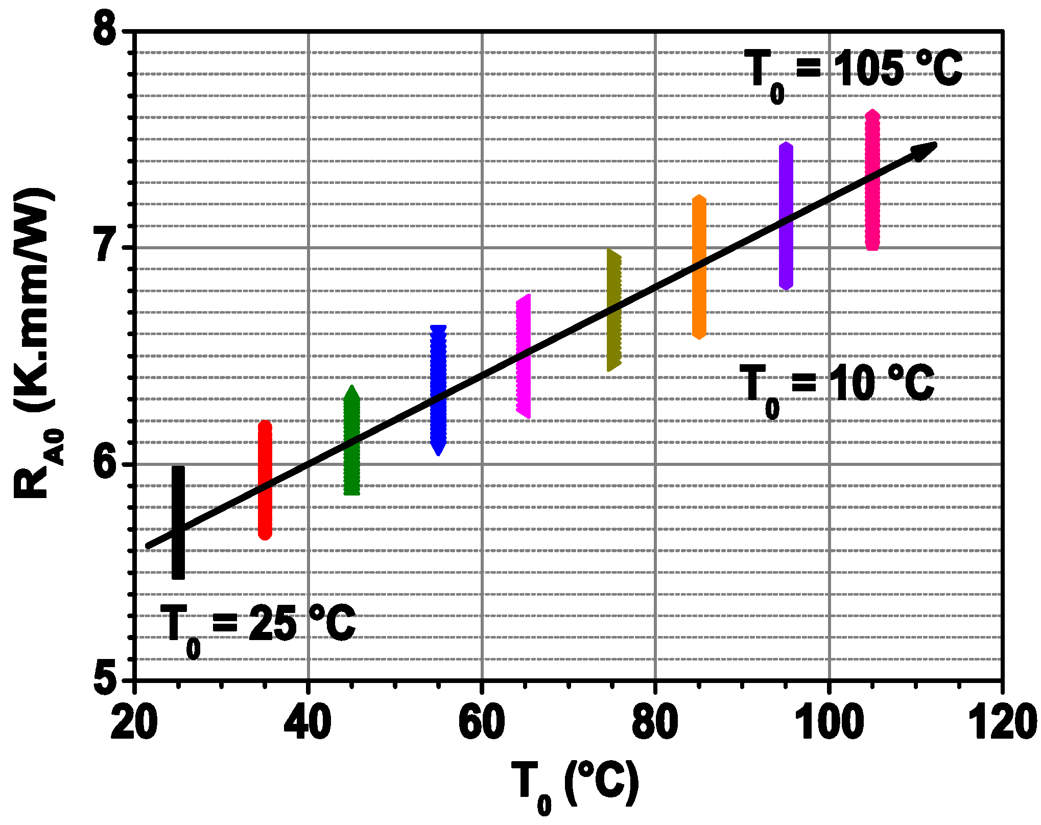
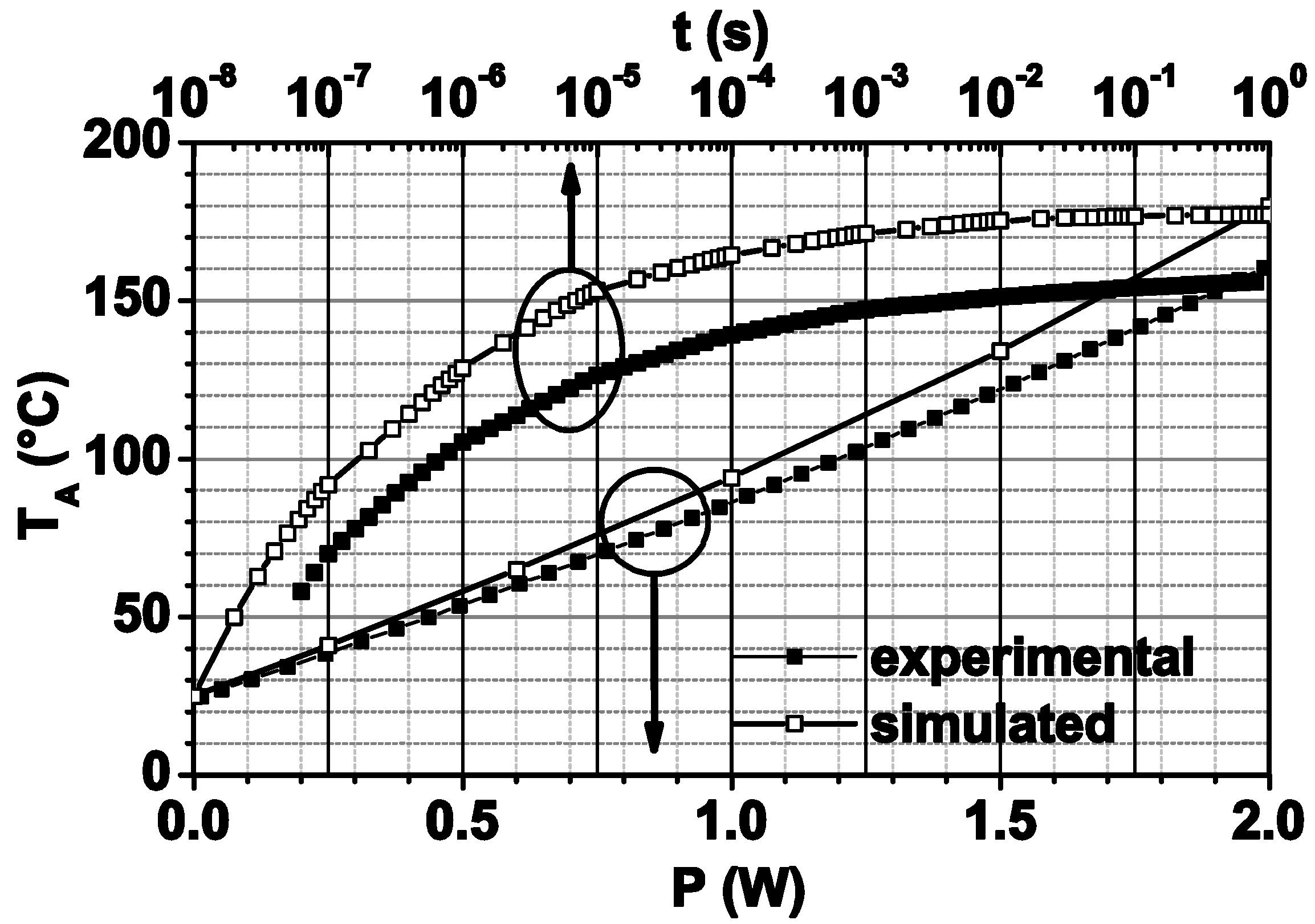
3.2. Average Channel Temperature Determination

The drain-source current IDS dependence on drain-source voltage VDS for gate-source voltage VGS = 0 V at varying ambient temperature T0 in the range of 25–105 °C was acquired during the VDS step, for a period of period ~1 s using the quasi-static operation as depicted in Figure 3. The maximum IDS obtained at the beginning of the extended VDS step ∆VDS ≈ 2 V, and subtracted by IDS value, that were acquired under quasi-static operation from the previous VDS step, results in dI0. Quasi-static and pulsed transfer I-V characteristics show soft gM and a gM0 decrease with rising VDS and T0 as illustrated in Figure 4. In particular, the VTH and VTHT were obtained from square rooted transfer I-V characteristics resulting in constant d V T H E / d V D S for a defined TA. Therefore d V T H E / d V D S ( d V T H d V T H N ) / d V D S is approximately d V T H E / d V D S k T H E ( T A T 00 ) + k T H 00 , T00 ≈ 25 °C, k T H E 8.8 · 10 6 K 1 and k T H 00 1.97 · 10 3 for TA (°C) in the saturation area. However, TA above T0 ≈ 105 °C was reached, which results in g M d V T H E / d V D S being linearly approximated, exhibiting variations of ~ 8·10−8°V/K in the range of 25–225 °C, corresponding to ~10% of d I T / d V D S . Interpolated thermal and isothermal parts of d I D S / d V D S vs. VDS at T0 ≈ 25 °C are depicted in Figure 5. Moreover, the dissipated power contribution d P * = V D S Δ I * , caused by dT0 for low VDS negligible in comparison with d P = V D S d I D S + I D S d V D S caused by dVDS, results in the simplified formula for differential thermal resistance RA0(T0) calculation [14] utilizing (12):
R A 0 = ( d T 0 * / d P ) ( d I d I 0 + g M d V T H E ) / Δ I *
The linear approximation T A T 0 R A 0 P , utilized in the first g M d V T H E iteration step in (15), leads to a formula resulting in RA0(T0) plot at different T0 and VDS as shown in Figure 6:
R A 0 = d I D S d I 0 + g M [ k T H E ( T 0 T 00 ) + k T H 00 ] d V D S ( Δ I * d P / d T 0 * ) ( g M k T H E V D S I D S d V D S )
Increasing VDS results in different RA0 values at a defined T0, which is partially caused by spatially distributed electrical parameters of the active device area such as the g M d V T H E / d V D S variation. The approximation R A 0 k R A ( T 0 T 00 ) + R 00 , T00 ≈ 25 °C, k R A 0.2   W 1 , R 00 57.0   K / W at the defined T0 was utilized to calculate TA in a recurrent way [14] as illustrated in Figure 7. In [8] the major contribution of the thermal IDS section is assigned to the serial source area resistance increase, caused by self-heating in a saturation regime for AlGaN/GaN HEMT. The simulated average channel temperature of the source to the gate area is in acceptable agreement in comparison to the calculated TA.
For the TA investigation of HEMT in the pulse operation, VGS and VDS bias was set to zero, superimposed by a VDS = 20 V pulse of length ~1 s. In the case of non-zero biasing, the initial condition of zero power dissipation is required to be satisfied. The period of ~5 s between voltage pulses was found sufficient because of the absence of the automated white LED illumination during the pulse breaks. The resultant current IDS acquired at T0 and delay t1 after the rising edge of constant amplitude VDS = 20 V and VGS amplitude sweeping from −4 V to −2 V at defined points, allowed us to plot the transfer I-V characteristics and to subsequently obtain the VTH dependent on t1 in the logarithmic scale in the range of 10−7–1 s, where the T0 step is set linearly in the range of 25–185 °C. Experimentally acquired IDS in the range of 20–100 ns and 25–185 °C for pulsed VDS = 20 V and zero VGS are depicted in Figure 8. Setting the VGS =−0.5 V allows us to obtain the supposed gM0 constant at the defined T0 due to a small deviation under isothermal conditions.
Although in the theoretical section the maximum IDS obtained at t0 ≈ 60–90 ns is suggested as the initial resultant current IDS0 at T0, simulation results exhibit higher TA than T0 by 30–50 °C at t0 which is caused by the rapid device self-heating. The real parasitic capacitance time constant and carrier transit time of the investigated device and measurement setup are the causes of this discrepancy. Linear extrapolation of IDS rising edge for t < t0 resulting in a linear dissipated power P increase, provides an opportunity to estimate IDS0 from d I T / k T = d T A ~ P utilizing the dIT sum as the quadratic time dependence. This approximation is found to be sufficient, although further VDS and IDS time dependence investigations for t < t0 are recommended. The trapping time constants of at least one order higher than ~10−7 s allow the calculation of the isothermal time dependence utilizing (14).
The intersection of the measured IDS time dependence and IE at defined T0 allows TA determination as depicted in Figure 7 and Figure 8. The difference between the TA obtained by the quasi-static and the pulsed measurements at t1~ 1 s can be explained by the partially compensated IDS during the rising time for the voltage pulse ΔVDS ≈ 20 V and the uncompensated IDS during the rising time at the voltage step ΔVDS ≈ 2 V, which were utilized in the quasi-static measurements. The difference of ~20 °C (13%) between simulated and experimental TA values is assigned to the different heat-flux distributions, resulting in the deviation between (5) and (6), as well as in the electric parameters from the source to the gate area, influencing dIT and IE approximation.

4. Conclusions

The average temperature significance was underlined in the theoretical section to avoid spatially distributed device parameters acquisition. The particular methods, based on an ambient temperature variation for a device under a quasi-static state and a device under pulse operation, were compared by taking the trapping process into account as a result of the FET threshold voltage shift that neglects electric capacitance. In the experimental section, the theoretical subtractions were adapted for the AlGaN/GaN HEMT channel temperature determination. The calculations were a result of the isothermal and thermal current sections separation, by taking into account the threshold voltage shift caused by trapped and free carrier concentration, the band diagram variation in operating temperatures and the applied voltage. The calculated and simulated average channel temperature ~160 °C of the source to the gate area for power dissipation ~2 W exhibits a difference of ~20 °C (13%). The considerations applied in the analytical model offer methodological consolidation for use in further research.

Author Contributions

Conceptualization, M.F., J.K.J. and A.C.; methodology, M.F.; software A.C.; validation M.F. and A.C.; device preparation, J.-C.J. and S.L.D.; writing—original draft preparation, M.F., J.K.J., J.K. and A.C.; funding acquisition, J.K.J. and J.K. All authors have read and agreed to the published version of the manuscript.

Funding

This work received funding from the ECSEL JU under grant agreement No 783274, project 5G_GaN2. The JU receives support from the European Union’s Horizon 2020 Research and Innovation Program and France, Germany, Slovakia, Netherlands, Sweden, Italy, Luxembourg, Ireland. This publication reflects only the author’s view and the JU is not responsible for any use that may be made of the information it contains. The work was also supported by Grant VEGA 1/0733/20 through the Ministry of Education, Science, Research and Sport of Slovakia.

Institutional Review Board Statement

Not applicable.

Informed Consent Statement

Not applicable.

Data Availability Statement

Data available on request from corresponding author.

Conflicts of Interest

The authors declare no conflict of interest.

References

  1. Ambacher, O.; Smart, J.; Shealy, J.R.; Weimann, N.G.; Chu, K.; Murphy, M.; Schaff, W.J.; Eastman, L.F. Two-dimensional electron gases induced by spontaneous and piezoelectric polarization charges in N- and Ga-face AlGaN/GaN heterostructures. J. Appl. Phys. 1999, 85, 3222. [Google Scholar] [CrossRef] [Green Version]
  2. Chattopadhyay, M.K.; Tokekar, S. Thermal model for dc characteristics of AlGaN/GaN HEMTs including self-heating effect and non-linear polarization. Microelectron. J. 2008, 39, 1181. [Google Scholar] [CrossRef]
  3. Doré, J.-B.; Belot, D.; Mercier, E.; Bicaïs, S.; Gougeon, G.; Corre, Y.; Miscopein, B.; Ktenas, D.; Strinati, E.C. Technology Roadmap for Beyond 5G Wireless Connectivity in D-band. In Proceedings of the 2nd 6G Wireless Summit (6G SUMMIT), Levi, Finland, 17–20 March 2020. [Google Scholar] [CrossRef]
  4. Chowdhury, S. Gallium nitride based power switches for next generation of power conversion. Phys. Stat. Sol. A 2015, 212, 1066. [Google Scholar] [CrossRef]
  5. Berthet, F.; Guhel, Y.; Gualous, H.; Boudart, B.; Trolet, J.L.; Piccione, M.; Gaquière, C. Characterization of the self-heating of AlGaN/GaN HEMTs during an electrical stress by using Raman spectroscopy. Microel. Rel. 2011, 51, 1796–1800. [Google Scholar] [CrossRef]
  6. Kuball, M.; Rajasingam, S.; Sarua, A. Measurement of temperature distribution in multifingerAlGaN/GaN heterostructure field-effect transistors using micro-Raman spectroscopy. Appl. Phys. Lett. 2003, 82, 124. [Google Scholar] [CrossRef]
  7. Kim, J.; Freitas, J.A.; Mittereder, J.; Fitch, R.; Kang, B.S.; Pearton, S.J.; Ren, F. Effective temperature measurements of AlGaN/GaN-based HEMT under various load lines using micro-Raman technique. Solid-State Electr. 2006, 50, 408–411. [Google Scholar] [CrossRef]
  8. Kuzmik, J.; Javorka, P.; Alam, A.; Marso, M.; Heuken, M.; Kordos, P. Determination of channel temperature in AlGaN/GaN HEMTs grown on sapphire and silicon substrates using DC characterization method. IEEE Trans. Electr. Dev. 2002, 49, 1496–1498. [Google Scholar] [CrossRef]
  9. Menozzi, R.; Membreno, G.A.U.; Nener, B.D.; Parish, G.; Sozzi, G.; Faraone, L.; Mishra, U.K. Temperature-dependent characterization of AlGaN/GaN HEMTs: Thermal and source/drain resistances. IEEE Trans. Dev. Mat. Rel. 2008, 8, 255. [Google Scholar] [CrossRef]
  10. Tarter, T.S. A Novel Circuit for the Evaluation of Thermal Impedance Characteristics of MOS Integrated Circuits. In Proceedings of the IEEE Semiconductor Thermal and Temperature Measurement (SEMI-THERM) Symp., San Diego, CA, USA, 7–9 February 1989; pp. 131–135. [Google Scholar] [CrossRef]
  11. Raj, B.; Bindra, S. Thermal Analysis of AlGaN/GaN HEMT: Measurement and Analytical Modeling Techniques. Int. J. Comp. Appl. 2013, 75, 4–13. [Google Scholar] [CrossRef]
  12. Synopsys. Sentaurus Device User Guide; v. L-2017.09; TCAD Sentaurus: San Jose, CA, USA, 2017. [Google Scholar]
  13. Heo, D.; Chen, E.; Gebara, E.; Yoo, S.; Laskar, J.; Anderson, T. Temperature Dependent MOSFET RF Large Signal Model Incorporating Self Heating Effects. In Proceedings of the IEEE MTT-S Int. Microwave Symp. Dig., Anaheim, CA, USA, 13–19 June 1999; Volume 1, pp. 415–418, ISBN 0-7803-5136-3. [Google Scholar]
  14. Florovic, M.; Kovac, J., Jr.; Kovac, J.; Chvala, A.; Weis, M.; Jacquet, J.C.; Delage, S.L. Models for the self-heating evaluation of GaN-based HEMT. Semicond. Sci. Technol. 2021, 36, 025019. [Google Scholar] [CrossRef]
  15. Chenming, C.H. MOS Transistor and MOSFETs in ICs—Scaling, Leakage and Other Topics. In Modern Semiconductor Devices for Integrated Circuits, 1st ed.; Prentice Hall: Midland Park, NJ, USA, 2010; Chapters 6 and 7; pp. 200–214, 266–269. ISBN 9780136085256. [Google Scholar]
  16. Florovic, M.; Szobolovszky, R.; Kovac, J., Jr.; Kovac, J.; Chvala, A.; Weis, M.; Jacquet, J.C.; Delage, S.L. Thermal analysis of AlGaN/GaN HEMT: Measurement and analytical modeling techniques. Semicond. Sci. Technol. 2019, 34, 065021. [Google Scholar] [CrossRef]
  17. Alim, A.A.; Rezazadeh, A.A.; Gaquiere, C. Temperature dependence of the threshold voltage of AlGaN/GaN/SiC high electron mobility transistors. Semicond. Sci. Technol. 2016, 31, 125016. [Google Scholar] [CrossRef]
  18. Florovic, M.; Szobolovszky, R.; Kovac, J.; Kovac, J., Jr.; Chvala, A.; Jacquet, J.C.; Delage, S.L. AlGaN/GaN HEMT channel temperature determination utilizing external heater. IEEE Semicond. Sci. Technol. 2020, 35, 025006. [Google Scholar] [CrossRef]
  19. Chvala, A.; Szobolovszky, R.; Kovac, J.; Florovic, M.; Marek, J.; Cernaj, L.; Donoval, D.; Dua, C.; Delage, S.L.; Jacquet, J.C. Advanced characterization techniques and analysis of thermal properties of AlGaN/GaN multifinger power HEMTs on SiC substrate supported by three-dimensional simulation. J. Electron. Packag. 2019, 141, 031007. [Google Scholar] [CrossRef] [Green Version]
  20. Chvala, A.; Marek, J.; Pribytny, P.; Satka, A.; Stoffels, S.; Posthuma, N.; Decoutere, S.; Donoval, D. Analysis of multifinger power HEMTs supported by effective 3-D deviceelectrothermal simulation. Microelectron. Reliab. 2017, 78, 148–155. [Google Scholar] [CrossRef]
Figure 1. Current time response I for (a) stepping Vn and (b) Vn pulse.
Electronics 10 02738 g001
Figure 2. Current time response comparison for various T0 for (a) Vn pulse and (b) time interval ∆t.
Electronics 10 02738 g002
Figure 3. Output I-V characteristics for VGS= 0 V at various T0.
Electronics 10 02738 g003
Figure 4. Transconductance gM, gM0 and threshold voltage VTH and VTHN dependence on VDS at various T0 required for trapping phenomena incorporation.
Electronics 10 02738 g004
Figure 5. Interpolated thermal and isothermal difference current sections dependence on VDS at T0 ≈ 25 °C.
Electronics 10 02738 g005
Figure 6. Temperature dependence of normalized thermal resistance RA0.
Electronics 10 02738 g006
Figure 7. Average channel temperature TA vs. dissipated power P in quasi-static state and TA time dependence for applied VDS pulse.
Electronics 10 02738 g007
Figure 8. Measured IDS time dependence (full-dot) at T0 ≈ 25 °C and approximated isothermal IE time dependence (empty-dot) at various T0 for applied VDS pulse.
Electronics 10 02738 g008
Publisher’s Note: MDPI stays neutral with regard to jurisdictional claims in published maps and institutional affiliations.

