Article

Design and Hardware Implementation of an IGBT-Based Half-Bridge Cell for Modular Voltage Source Inverters

by
Roberto Morales-Caporal
*,
José F. Pérez-Cuapio
,
Haydee P. Martínez-Hernández
and
Raúl Cortés-Maldonado
National Technological Institute of Mexico/Technological Institute of Apizaco, Av. Instituto Tecnológico s/n, Apizaco C.P. 90300, Tlaxcala, Mexico
*
Author to whom correspondence should be addressed.
Electronics 2021, 10(20), 2549; https://doi.org/10.3390/electronics10202549
Submission received: 15 August 2021 / Revised: 31 August 2021 / Accepted: 1 September 2021 / Published: 19 October 2021
(This article belongs to the Section Power Electronics)

Abstract

:
This article presents the design and hardware implementation of an IGBT-based half-bridge voltage source inverter (VSI) to be used as a basic cell to assemble VSIs of different topologies in modular ways. Herein, we have presented the design methodology and utilized techniques for reducing stray inductances and EMI radiation on the printed circuit board, as well as the way to calculate and select the main electronic components. For the design of the circuit board, local regulations for grid interconnection and international standards were considered in order to obtain a safe and reliable electronic power cell. The developed hardware was subjected to different tests using AC electric motors as loads to validate its design. Two VSIs topologies were evaluated: a single-phase two-level full-bridge inverter and a three-phase two-level inverter. The experimental results validated the theory and demonstrated the excellent performance, reliability, and high efficiency of the developed half-bridge power cell for modular VSIs.

1. Introduction

A power inverter converts a direct current (DC) source at its input into an alternating current (AC) output waveform [1]. The AC power at the output has a fundamental component with adjustable frequency and amplitude. According to the type of AC output waveform, the inverter topology can be considered a voltage-source inverter (VSI), where the independently controlled AC output is a voltage waveform, or as current-source inverter, where the independently controlled AC output is a current waveform [2]. VSI topologies are the most widely used because they naturally behave as voltage sources, as required by many electrical applications, such as: variable speed electrical drives, electric vehicles, active power filters, uninterruptible power supplies, power generation from renewable energy sources, etc. VSIs can be built with any number of output phases, but in practice, single-phase and three-phase inverters are most common [1,2]. Different design approaches address various issues that may be more or less important depending on how the VSI is to be used.
Researchers continually develop different VSI topologies to achieve an increase in reliability, performance, efficiency, and a reduction in cost and size, always considering the application of the inverter [3]. Lately it has become particularly desirable to have a certain degree of modularity for reasons of replaceability and scalability [4]. Modularity, in this case, refers to a technique for comparably building a large power inverter by combining (in series and/or parallel connections) identical smaller subsystems, called power cells [5]. The assembly of modular VSIs using power cells formalizes the idea that reliability can be improved while reducing operating cost. Moreover, this technique allows the possibility of assembling multilevel inverters (MLIs) [6]. The basic concept of MLI is that it uses several low-rated power semiconductor switches (PSSs) for synthesizing a stepped voltage waveform for achieving higher power levels.
There are different topologies of power cells proposed in the literature, but the most common are the half-bridge (HB) inverter and the full-bridge (FB) inverter, as shown in Figure 1a,b, respectively [6,7].
The HB inverter shown in Figure 1a was composed of two PSSs (in this case, represented by IGBTs) and two diodes. The freewheeling diodes are required to provide continuity of current for inductive loads. This power cell can operate in two quadrants and can generate only two voltage levels at the output, as shown in Figure 1a [2]. The PSSs T1 and T2 cannot be on simultaneously because a short circuit across the DC-link voltage source (Vdc) would be produced. The states for the PSSs T1 and T2 are defined by the modulating technique, which in this case can be a carrier-based Sinusoidal Pulse-Width Modulation (SPWM). On the other hand, the FB inverter, which is built with two identical HB cells can generate positive, zero and negative output voltages, as shown in Figure 1b, hence, the output voltage (vo) of the FB inverter is twice that obtained with the HB topology. This implies that, for the same power, the output current and the switch currents are one-half of those for a HB inverter. As expected, both PSSs T1 and T2 should not be on at the same time, nor T3 and T4. Otherwise, a short circuit would exist across the DC source.
In order to avoid the short circuit or an undefined AC output voltage condition, the modulating technique should ensure that either the top or the bottom PSS of each leg is off at any instant. Several modulating techniques have been developed for single-phase FB inverters. Among them are the bipolar and unipolar SPWM techniques.
A full explanation of the operation, switch states, control techniques and output waveforms of the HB and of the FB inverters are beyond the scope of this article; however, they can be consulted in [1,2].
From Figure 1a it can be seen that a branch of the single-phase FB or of the three-phase inverters are identical to a HB cell. For this reason, in this work, an HB cell was designed and implemented to be able to assemble other VSI topologies in a modular way.

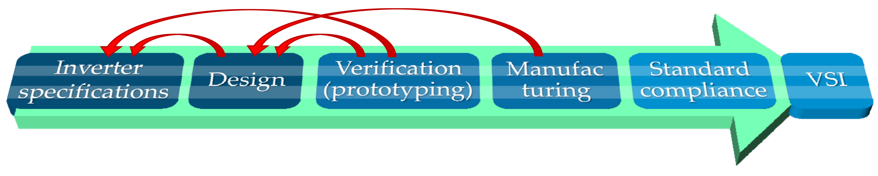
2. A Review on Power Converter Design Methodologies

In recent years, several research groups have proposed design workflows for the design and implementation of power converters. Currently, all of them inherently include the use of computer-aided design (CAD) tools [4]. They can be summarized in four main groups: traditional design (TD) [8,9,10], design for reliability (DFR) [11,12,13], multi-objective design optimization (MODO) [14,15,16,17], and automated design (AD) [8,16,17,18,19,20].

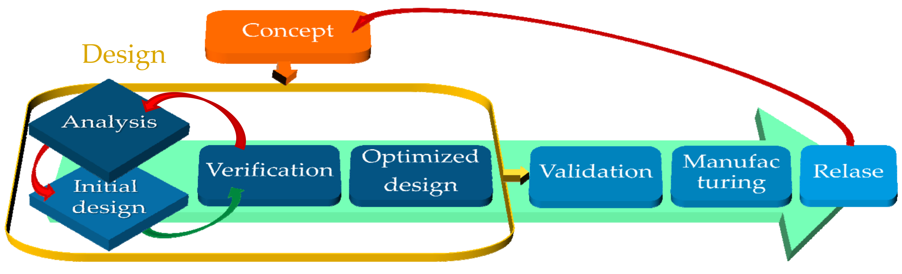
2.1. Traditional Design

Power converters are traditionally designed following the main steps shown in Figure 2. A brief explanation of these steps is given below:
Specifications: All specifications, including function, power density, shape, and weight must be clear, well defined and approved by the lead designer. This also includes application requirements such as efficiency, price, and standards compliance.
Design: The power levels are calculated based on the operating temperature and switching frequency. Then, the circuit schematic is designed. The components are selected, considering power level, reliability, cost, and functionality. Designers must take care of the physical arrangements of the converter and the positions of the components on the PCB. Housing, cooling techniques, and packaging must be defined according to operating conditions. In case of any unforeseen requirement or specification that prevents the conclusion of this stage, the designer returns to the previous stage [9].
Verification (prototyping): A prototype is usually implemented to verify if the design is in accordance with the specifications and the targeted performances. If the specifications are not achieved, or if the performances are below expectations, the designer must take some steps back and carry out a rework of the design itself [9].
Manufacturing: In this phase, the availability of components is verified, along with the manufacturing complexity. The layout and position of components may be modified to ease the assembly process. In addition, some tests to evaluate the design are carried out.
Standard compliance: The developed inverter must be tested for standard and regulation compliance before entering into mass production.
Advantages: This is the lowest-cost design process. It is easily replicable and easily accessible. It can be used for the development of specific purpose converters.
Disadvantages: No optimization algorithm is considered. It is the least reliable methodology. Sometimes, more than one prototype must be manufactured, and it is possible to fall into a repetitive design cycle, resulting in increased development time.

2.2. Design for Reliability

The DFR procedure is shown in Figure 3. It designs reliability into each stage of the process (i.e., concept, design, validation, production and release), especially in the design phase. Design tools applied in the design stage according to the initial design concept are explained below. A more comprehensive study of its workflow can be found in [12].
Concept: In the initial phase, the relevant conditions to which the converters are expected to be exposed (i.e., mission profile) are identified. Benchmarking of system architecture and circuit topology is conducted.
Analysis: The analysis covers the following four aspects: (a) basic operation of the power converter; (b) electrical and thermal stress analysis based on the system specifications and mission profile for preliminary selection of components; (c) failure mode effect and analysis to identify the failure mechanisms [13], and (d) list of reliability critical components in the system.
Initial design: Multi-domain simulation, especially the electrical-thermal simulation, is a very useful tool to virtually investigate the static and dynamic properties of the system to be designed. The link between the electrical domain and thermal domain is the power loss and thermal model of individual component, and fault tolerant design is considered.
Verification: At this stage, a prototype of the converter is implemented for testing, including: highly accelerated limit testing, multi-environment over stress testing, test data analysis, reliability and durability degradation analysis.
Optimized design: At this stage, some optimization technique is used for one of the design goals (reliability, availability, lifetime, robustness, efficiency, power density, etc.).
Advantages. The design is based on the mission profile, taking into account the large parametric variations. Fault tolerant design and well suited for mass production.
Disadvantages: In a typical case, optimization is carried out for one manufactured prototype and one specific control procedure. A virtual prototype is required for the optimization process. It has only been used in the design of PSS modules.

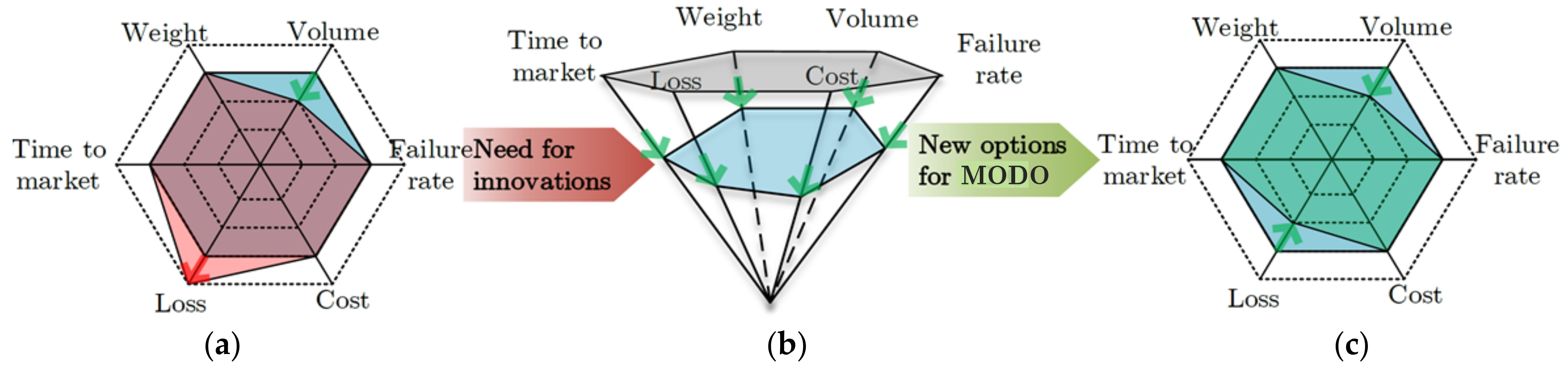
2.3. Multi Objective Design Optimization

The MODO method is based on mathematical multi-physics models of the system. The optimization objectives are efficiency, converter volume, and costs. The ultimate goal of the approach is the determination of the Pareto fronts, i.e., the absolute performance trade-off limits for a given set of converters building blocks (topologies, control schemes and components). Regarding the optimization of power converters, a fundamental observation is the fact that typical primary performance measures (but also general performance measures) are coupled, i.e., inherent trade-offs complicate the concurrent improvement of multiple or all performance measures. Consequently, single-objective optimizations should be avoided as the aggressive improvement of a particular performance measure will usually result in poor performance regarding other performance measures [16].
The fundamental trends for the development of power electronics converters are shown in Figure 4a [16,17]. As mentioned above, the performance indices considered in the design of power converters are mutually coupled, e.g., high power densities imply high frequencies, which potentially lead to a reduction in efficiency due to physical barriers and technology constraints (as a result, there is a constant demand for new PSS technologies, new circuit topologies, and modulation schemes, etc., to reduce these barriers). These limits are realized through mathematical modeling and subsequent multi-objective optimization of converter systems.
Figure 4b shows the performance trends over time. As technology improves and innovation occurs, there will be more options available in design optimization which will allow for all requirements to be met simultaneously (see Figure 4c) [17].
The MODO methodology can actually be included within the AD technique, since once the topology and the application of the converter are known, it can be designed automatically, thanks to a software that contains a prototyping subroutine that generates a digital twin prior to the manufacture of the physical prototype. A simplified workflow of the prototyping routine of the MODO-based design process is shown in Figure 5 [16].
Advantages: MODE-based procedure can be totally automated. Different design objectives can be included. Facilitates the systematic design and the concurrent optimization with respect to the efficiency, volume, and the component costs.
Disadvantages: Design cost increases. Software for modeling and simulation is required. An exact virtual model is required (digital twin), which can be hard to carry out.

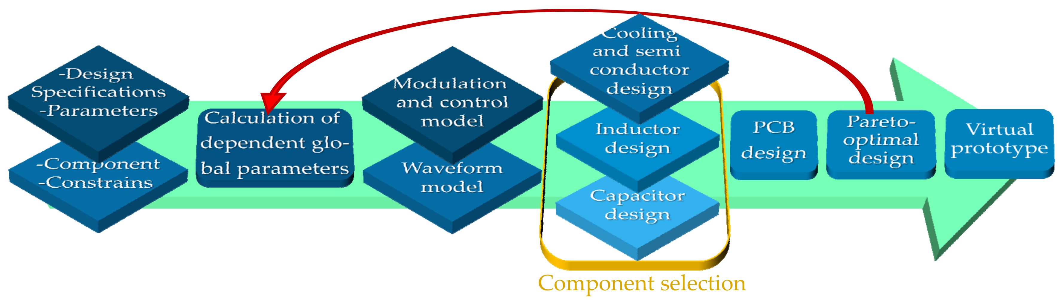
2.4. Automated Design
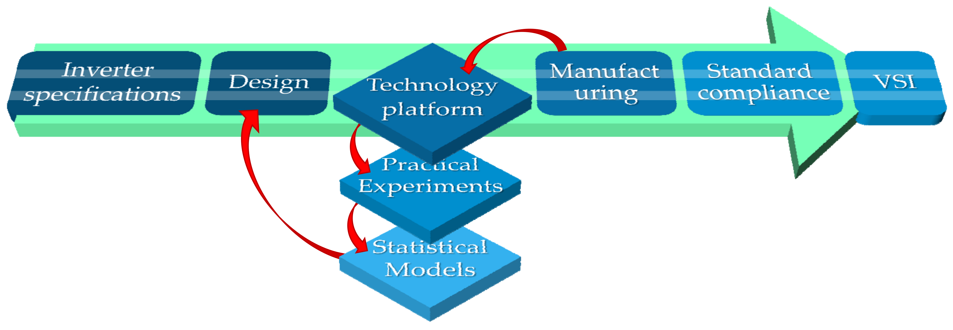
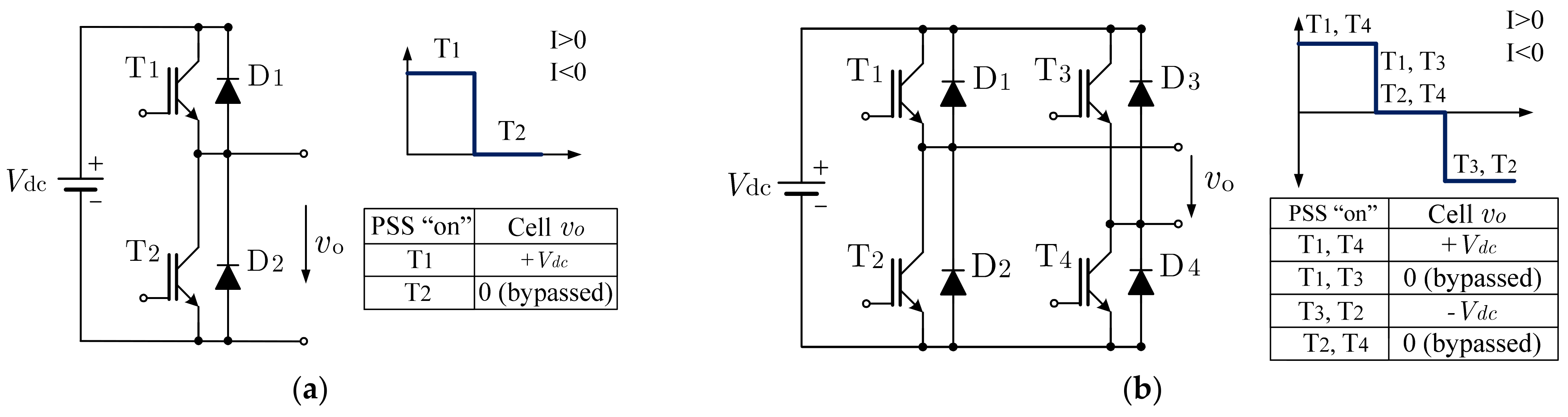
In contrast with DFR and MODO methods, the AD method does not aim to create an optimal solution for the power converter. Instead, it proposes a viable solution, with a reliable prediction of efficiency and operating temperature. The performance levels of the designed power converter are not defined by an optimization at converter-level design but by an overall optimization of the technology platform characteristics [19].
Figure 6 shows a simplified workflow of the AD method. A set of technology platforms must be made available to cover a wide range of options, applications, and targeted performances. Once each of these technology platforms are characterized and modeled, a database is built for each platform with many parameters and characteristics made available for design and selection routines. Based on machine learning, the characteristics are extracted from existing and representative power converter arrays and conversion standard cells, providing accurate prediction models [20].
Based on these highly accurate models, a straightforward design and selection approach can be carried out from the specifications of the desired VSI through a virtual prototyping phase (as done in MODO methodology). First, the converter specifications are compared to the characteristics of each technology platform. Then, the possible solutions are identified in each phase of the technology platform compliance. Various configurations and architectures are virtually prototyped to identify the one with the best characteristics. Finally, in the space of all possible solutions, the designer identifies the best option to be produced.
Advantages: It is very suitable for mass production. The development time is reduced. The strategy can be applied to design VSIs based on modules or discrete devices.
Disadvantages: Design cost increases. Software with artificial intelligence techniques is required. It is not suitable for custom designs.

3. Background

3.1. Development Purpose and Contribution

Although nowadays, power cells and even MLIs of different levels and topologies can be found on the market [21], in developing economies, it is still difficult to obtain or assemble modular VSIs to alleviate some of the problems that commonly appear in rural power generation facilities from unconventional source, such as:
  • Low power generation facilities with renewable sources of different power levels can be found, and it is difficult to obtain different VSIs for each installed power level. Additionally, in case that the installed power is modified, the VSI must also be changed.
  • Many times, a VSI of adequate power is not available on the local market and an oversized VSI is installed, resulting in an excessive investment cost.
  • Sometimes the VSIs do not comply with local grid regulations and standards (operational issues and/or design issues), which can limit their use [22].
  • It is difficult to find single-phase VSIs (with or without interconnection capacity) for small customers/generators (homes, workshops, shops, health centers, rural schools, etc.) than three-phase VSIs for large consumers (industry, electric traction, etc.).
  • Researchers and educators still find it expensive to build unconventional converter topologies with commercial hardware for research and teaching purposes.
This work aimed to contribute to the acceleration of solutions to the aforementioned inconveniences. Furthermore, it is well known that power electronics is one of the key technologies to address real-life issues in energy access and its utilization.

3.2. Design Considerations

Having identified the problems to be solved—and considering that the converter will have home and laboratory applications—it was concluded that the main design objectives were low cost and high functional performance [3].
Other important design considerations that were taken into account include:
  • Low consumption and reduced EMI
  • High efficiency and reliability.
  • Modularity and reduced size.
  • Local grid regulations and international standards.
  • Natural convection cooling

4. Design Process

4.1. Specifications and Key Components Selection

4.1.1. DC-Link Capacitance

The output power rating of the VSI will be determined by the number of used HB cells and by its final topology. In single-phase HB and FB inverters, the capacitor design is crucially determined by the load current [23]. Thus, for the HB cell a maximum output current of io = 25 A (rms) and switching frequency of fSW = 10 kHz has been considered, to keep low the power dissipation losses. A single-phase utility grid of vs = 120 V (rms) before rectifier is also consider as input.
When using SPWM techniques and neglecting the DC-link voltage oscillation compared to its average value, the single-phase VSI output voltage, averaged over a switching period TS = 1/fSW, can be calculated within a linear modulation range as [24]
v ¯ o t = m V d c sin w t ,
being t the time, w the angular fundamental frequency, and m is the modulation index (m = Vo/Vdc). Neglecting the switching ripple, the nominal output current of the VSI can be expressed as a sinusoid as follows
i o t = I o sin w t φ ,
where Io represent the maximal output current amplitude and φ its phase angle compared to the voltage.
On the other hand, the maximum voltage ripple on DC-link in one switching period is calculated by [24]
Δ v d c max = max Δ u d c min Δ u d c ,
since this voltage ripple is linearly proportional to the Io and to TS, a voltage switching ripple coefficient (Δrmax) can be defined to simply the analysis, as
Δ r max = C d c Δ v d c max I o T S .
Δrmax is numerically calculated under different scenarios, and depends on the angle of reference voltage wt, which ranges from 0 to 2π within a single fundamental period.
Under sinusoidal PWM in one fundamental period, Δrmax = 0.2165, which occurs at m = 0.5 and φ = π/2 [24,25]. Thus, if Ts = 100 μs and the Δ v d c max = 5 V is considered, the minimum DC-link capacitor for this application can be dimensioned as
C d c 0.2165 I o T S Δ v d c max = 0.2165 25 2 100 e 6 5 = 153.08   μ F .
This is the minimum capacitance value. Therefore, in this work, a higher capacitance value was selected, but considering that the volume, weight, and cost remain within acceptable ranges. Two electrolytic capacitors connected in parallel of C = 390 μF and 600 V have been used to keep the voltage ripple smaller than 5 V for two-level VSIs.

4.1.2. Power Semiconductor Switches (PSSs)
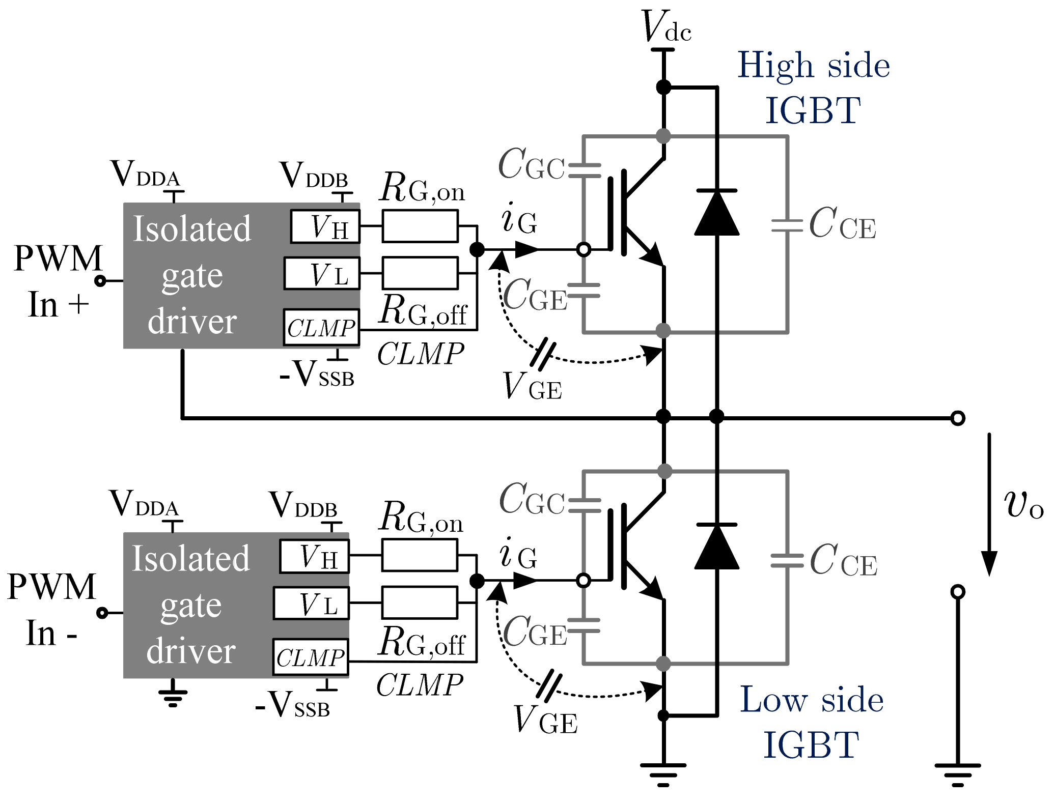
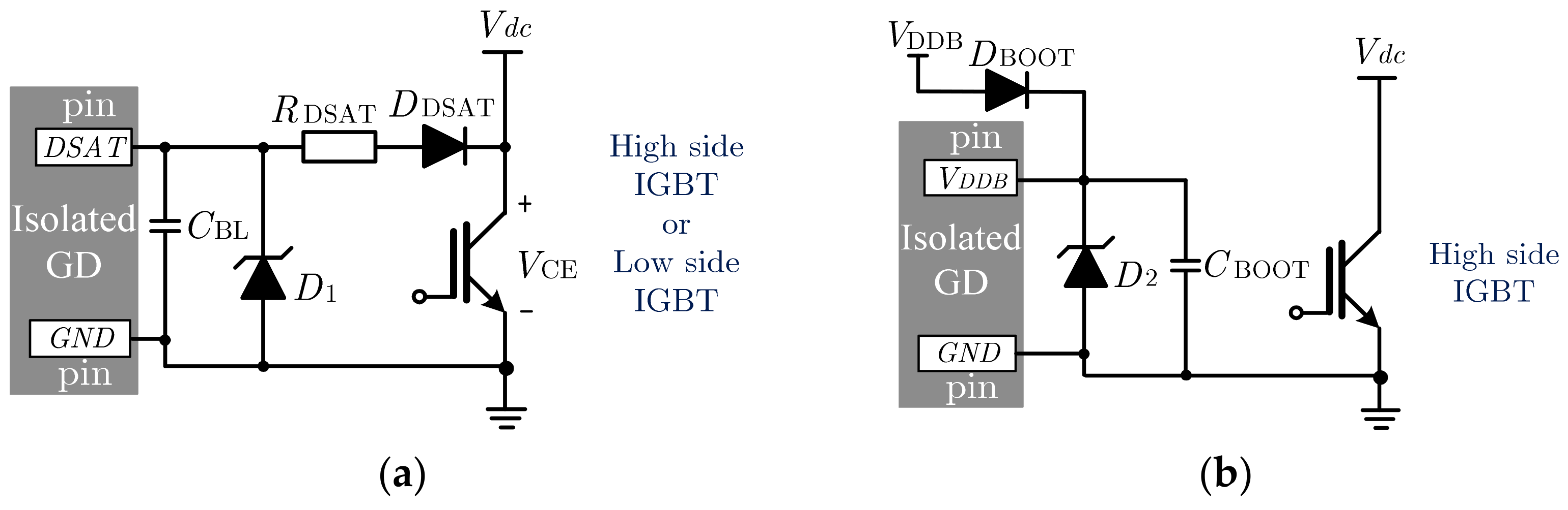
Nowadays, the insulated-gate bipolar transistor (IGBT) is typically the PSS of choice for assembling low-cost, medium-frequency VSIs, since IGBTs have some key advantages over metal-oxide-semiconductor field-effect transistors (MOSFETs) [26]. On the other hand, and according to the indicated applications, a common IGBT is much cheaper than either a siC-IGBT or a GaN-IGBT.
Thus, considering the voltage level and the application (hard switch), a punch-through technology is preferable [27] and an ultra-fast freewheeling diode must be included; a discrete device (IGBT+diode) is selected. This allows designers to build a more economical VSI since discrete devices are cheaper than modules.
The specifications of the designed power cell are shown in Table 1.

4.1.3. Gate Driver

In HB configuration, as shown in Figure 7, the high-side IGBT and the low-side IGBT rapidly toggle the load’s connections between positive and negative poles of the DC-link.
Driving the gates of these IGBTs is essential to maximizing efficiency by making them behave, as much as possible, like ideal switches. Figure 7 also shows isolated gate drivers (GDs) to separate a low-voltage system controller from the high-voltage power stage. The other essential functions of the GDs are to amplify control signals and to give to the high-side control signal a reference ground with separate power domain.
After conducting a detailed analysis between the different gate drivers for IGBTs with the characteristics according to the present design, and above all looking for an acceptable cost, the Si8285 by Silicon Labs was selected [28].
IGBT Switching behavior: IGBT’s turn-on and turn-off depend on the voltage between gate and emitter (VGE), due to the parasitic input capacitance (CGE) and the Miller capacitance (CGC), as depicted in Figure 7 [29]. CGE and CGC require the design of certain circuits for rapid charge and discharge during switching. In this design, an isolated GD with separated output pins was selected to allow independent setting of the switch’s turn on and off times. This capability is quite helpful in HB cell configuration where the speed of the turn-on and -off are aligned to minimize shoot-through current [29,30]. The low-impedance Miller clamping pin (CLMP) attenuates the Miller voltage spikes and renders the driver with three output pins more suitable for driving high power IGBT with larger input gate (CGE and CGC) parasitic capacitances. The explanation of the turn-on and -off characteristics of the IGBT can be found in [28,29,30] and will no longer be explained here.
Turning the power switch on and off requires current flow to charge and discharge the gate capacitors. Commonly, the datasheet provides the total gate charge (QGtotal) required to switch a device between the on and off positions. Equation (6) defines the relationship between the iG, the total gate charge Qtotal, and the switching transition time t.
Q total = i G t .
Gate resistors: The switching transition time depends on how quickly the total gate charge QG is delivered, which in turn, depends on the amplitude of the iG. Therefore, transition times (trise and tfall) can be controlled by selecting the values of the gate resistors to a desired gate current levels [28]. From Equation (6) and the turn-on and -off characteristics, the iG required to switch the IGBT between the on and off states can be approximated:
i G , on = Q G t rise ,   i G , off = Q G t fall .
Then, the gate resistors can be calculated using Ohm’s law and the driver’s operating voltage [31] as
R G , on = V H I G , on R 0 G , on ,   R G , off = V L I G , off R 0 G , off ,
where R0G,on and R0G,off represent the internal source impedance of the gate driver when on and off, respectively. The voltages VH and VL must be calculated from the voltage VDDB, and its respective reference when on and off, since the gate voltage from the on state (sustained by gate capacitors) needs to discharge to 0 V to turn off the power device.
Desaturation detection: The GD provides sufficient voltage and current to drive and keep the IGBT in saturation during on time to minimize power dissipation and maintain high efficiency operation. However, under abnormal load conditions (i.e., when load has low impedance), it can force the switch out of saturation and cause permanent damage. To protect the IGBT during abnormal load conditions, GD shuts down the driver upon detecting the fault, and provides a fault indication to the controller. Figure 8a illustrates the Si8285 de-saturation circuit, which has been designed with help of the datasheet. Due to the parasitic inductance of the VSI, voltage spikes are generated during high current switching. Therefore, it is prudent to add a Zener diode (D1) from GND pin to DSAT pin.
Bootstrap circuit: When using HB configurations, it is necessary to generate high-side bias to drive the gate of the high-side MOS referenced to the switch node. One of the most popular and cost-effective ways for designers to do so is through the use of a bootstrap circuit which consists of a bootstrap capacitor (CBOOT), a bootstrap diode (DBOOT), and a current limiter resistor, which was omitted in this design. Figure 8b shows a simplified bootstrap circuit diagram. The operation and design of this circuit is explained in [32].
Dead-time: For VSI circuits, it is necessary to set an on-off timing delay (dead-time) in order to prevent short circuits. During the dead-time, both the upper and lower arms are in the off state. It is important to be careful with the dead-times recommended by the datasheet. An appropriate dead-time should be settled by confirming the power level to be handle [30]. In this work, a dead time of 2.3 µs was programmed and compensated as recommended in [33].
Power consumption: When all the circuit components of the GD are calculated, it is important to review the total power dissipation of the driver’s package to ensure that the maximum junction temperature of the GD is not exceeded while operating within the desired temperature range. Power consumptions should be calculated with assistance of the technical datasheet, to prevent the driver exceeding the power consumption rating.
Fault and reset: The FLT pin is an open-drain output. A 10 kΩ pullup resistor is used to make it rise more quickly and to provide logic high when FLT and RDY are inactive. Fast common mode transients can inject noise and glitches on FLT and RDY pins due to parasitic coupling. This is dependent of the board layout. In this case, an additional capacitance of 100 pF was included on the FLT and RDY pins. Other protection circuits recommended by the manufacturer were also considered in the present design.
Table 2 summarize the bill of materials of the designed HB cell board.

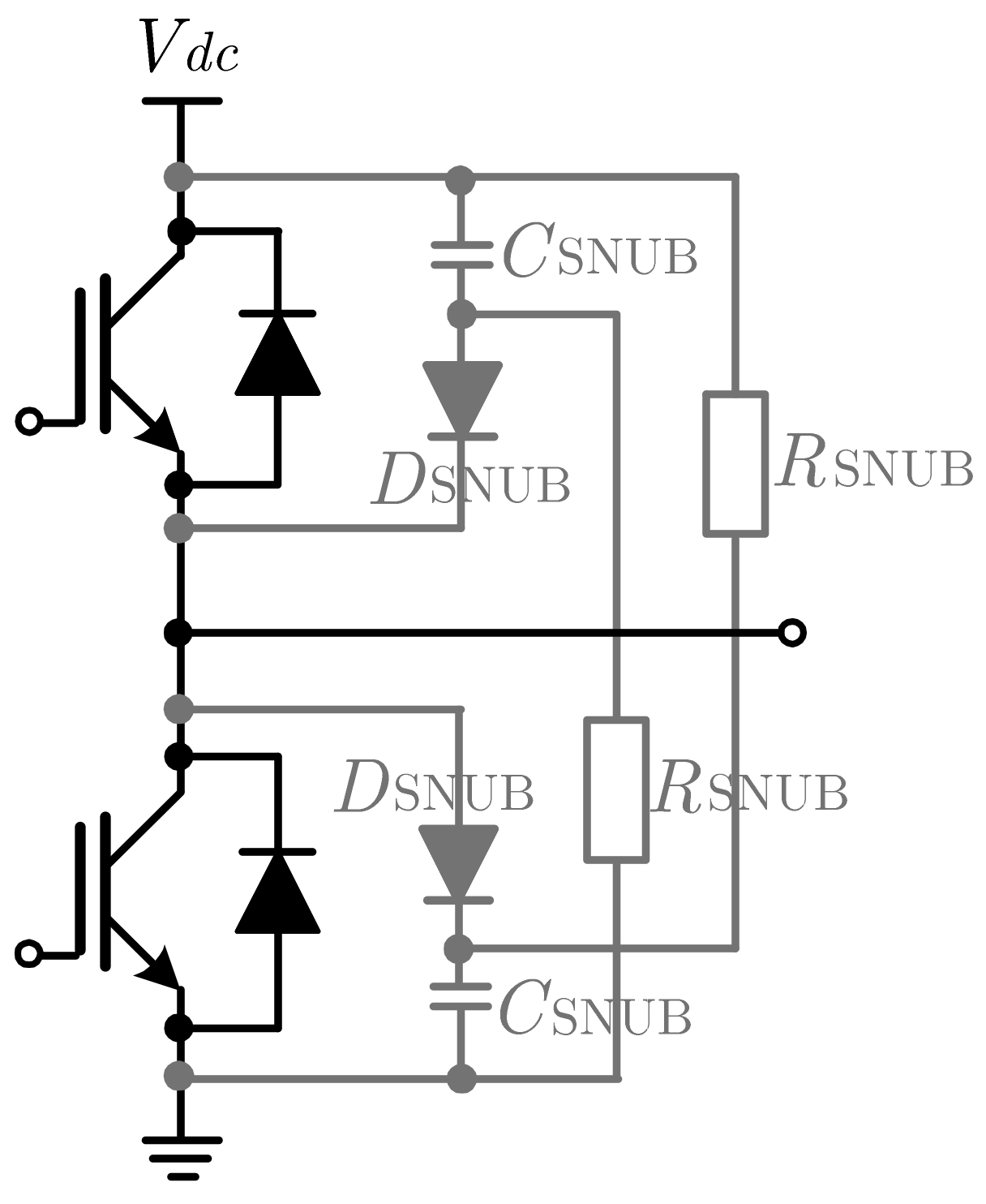
4.2. Snubber Circuit
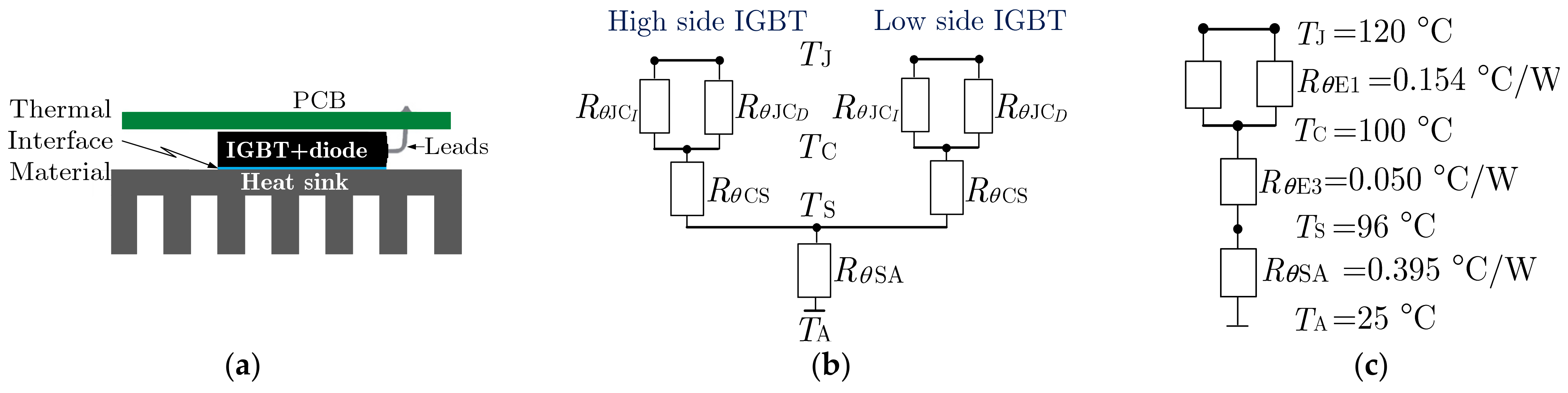
Peripheral parasitic inductance (Ls) of the VSI induces ringing when power device switching. The voltage over Ls is expressed by following
V L s = L s d i d t .
Snubber circuits are commonly used to suppress ringing. The discharge-suppressing RCD snubber circuit shown in Figure 9 was implemented in this work because of its lower-power consumption. The snubber capacitor (CSNUB) absorbs ringing through the snubber diode DSNUB at turn off. The excessive noise is consumed by the snubber resistor (RSNUB) during off. The snubber does not suppress ringing at turn-on because DSNUB keeps current conducting only in one direction, and thus saves energy.
The RSNUB and CSNUB parameters of the snubber can be approximated as [34]
C SNUB = L S I o f f 2 V P S V dc 2 ,   R SNUB 1 2.3 C SNUB f S W .
The calculated and the used snubber parameters are shown in Table 3.

4.3. Heat Sink

In power converters, heat sinks are used to move heat away from the devices in order to maintain a lower temperature. Before conducting the heat sink selection process, common terms were defined, and the concept of a thermal circuit was established.
PD: total power or rate of heat dissipation in W.
TJ: maximum junction temperature of the device in °C.
TC: case temperature of the device in °C.
TS: sink temperature in °C.
TA: ambient air temperature in °C.
Using temperatures and the rate of heat dissipation, a quantitative measure of heat transfer efficiency across two locations of a thermal component can be expressed in terms of thermal resistance Rθ, defined as [35]
R θ = Δ T P D ,
where ΔT is the temperature difference between the two locations. The unit of thermal resistance is in °C/W, indicating the temperature rise per unit rate of heat dissipation.
In this case, the two packages (IGBT+diode) were mounted on a common heat sink, leaving a small space between the device and the PCB as shown in Figure 10a. Then, using the concept of thermal resistance, a thermal circuit of this system can be drawn, as shown in Figure 10a,b. In this thermal model, heat flows from each junction of each case, then from each case across similar interface material into the common heat sink. Finally, the heat is dissipated from the heat sink to the ambient air.
The thermal resistance between the junction and the case (RθJC) of one package is given by the manufacturer, thus from Table 2 and Figure 10b, the total RθJC of a package (IGBT+diode) is
R θ E 1 = 1 1 / R θ JC I + 1 / R θ JD D = 1 1 / 0.2 + 1 / 0.67 = 0.154   ° C / W .
According to the package datasheet, PD = 625 W when TC = 25 °C, Thus
T J = R θ E 1 × P D J C + T C = 0.154 × 625 + 25 = 121   ° C .
For the design process TJ = 120 °C and TC = 100 °C have been considered. From Equation (11), and considering the same TJ and TC in both package (see Figure 10c), the dissipated power by the two devices can be evaluated as
P D E 1 = T J T C 1 / 1 / R E 1 + 1 / R E 1 = 20 0.77 = 259.740   W .
In Figure 10b, RθCS represents the thermal resistance across the interface between each device case and the common heat sink, depending on the surface finish, flatness, applied mounting pressure, and contact area [35]. In this case, according to the used material (thermal grease) RθCS = 0.1 °C/W. The RθSA represents the heat sink thermal resistance, which should be determine for the heat sink selection.
In this design, a difference of 4 °C between TC and TS was considered, as mentioned in [36]. Thus TS = 96 °C and if a TA = 25 °C is selected the dissipated power by the heat sink is
P D E 3 = T J T C R θ E 3 = 4 0.050 = 80   W ,
now the RθSA can be calculated with the help of the power to be dissipated as
P D S A = 259.740 80 = 179.74   W ,
R θ SA = ( 96 25 ) 179.74 = 0.395   ° C / W ,
the maximum RθSA required of a heat sink for this application. Therefore, for a TJ = 120 °C and two packs mounted on the same heatsink, since natural convection cooling is desired, a 193AB1500B heat sink may be useful. Nevertheless, a smaller heat sink can be selected if a forced cooling is considered.

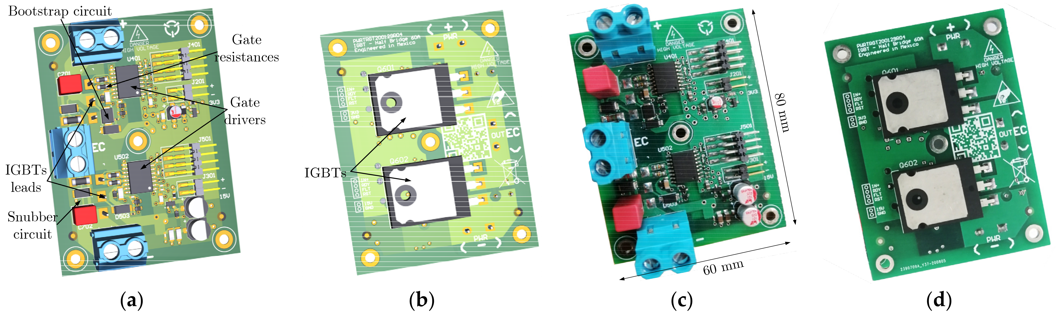
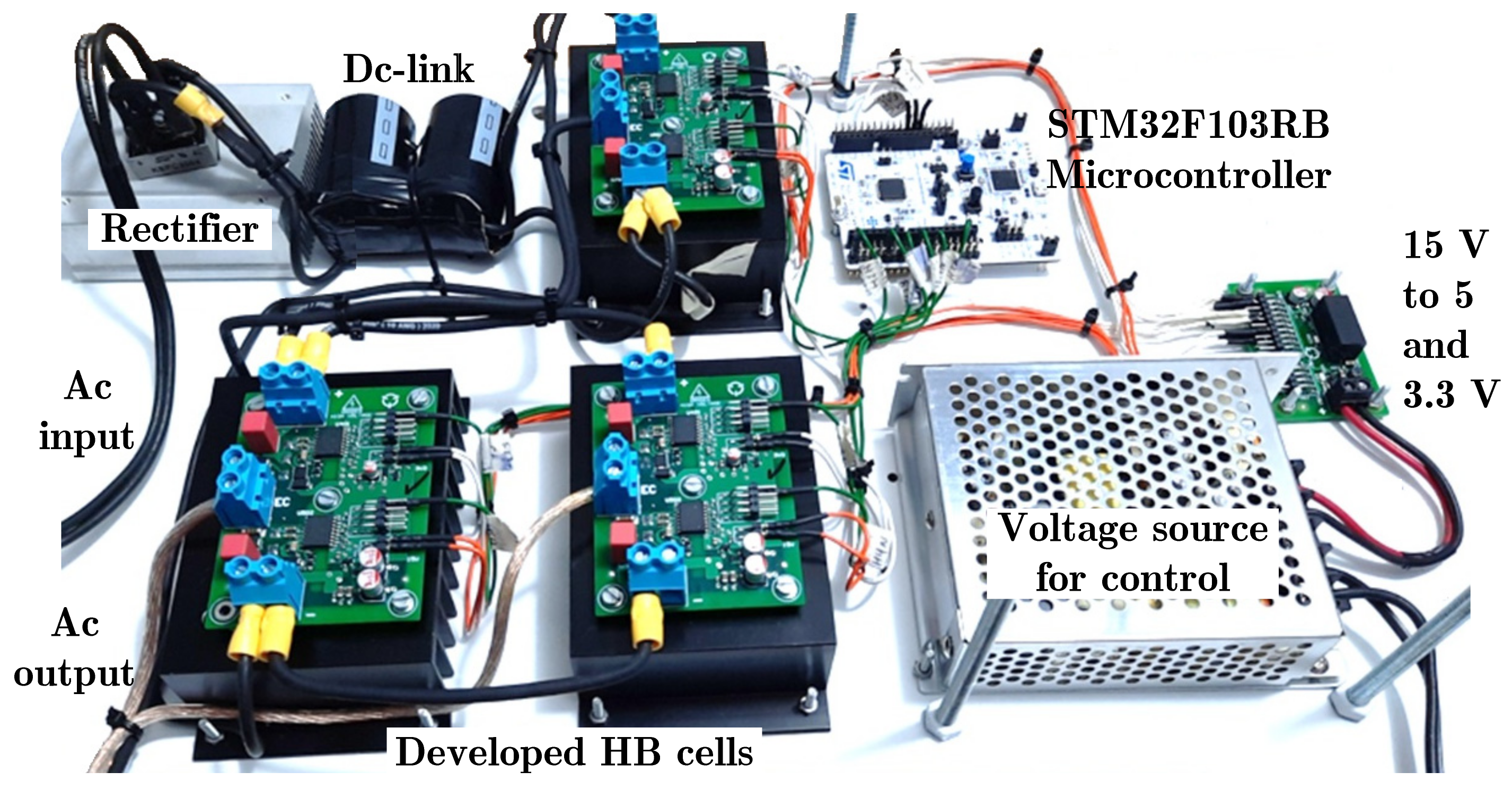
5. Hardware Implementation and Results

5.1. PCB Design

5.1.1. Standards

The PCB was designed considering some international electronic design standards, such as IPC-2221, IPC-2231, IPC-2152 and IPC-D-325A [37]. The IPC-2221A recommends a series of standard sizes to be more efficient with the number of boards that can be manufactured at the same time. To keep the board size as small as possible, 4 layers and 2 oz copper PCB is selected. The price of a PCB layout can increase considerably when the board size exceeds 100 mm × 100 mm. Therefore, in this design, a dimension of type A1 was selected (60 mm × 80 mm).
Fashioning the design according to article 705 of NOM-001 (Mexican standard) for interconnection to the national electrical network was also considered [38].

5.1.2. Design Considerations for Low Stray Inductance and Reduced EMI
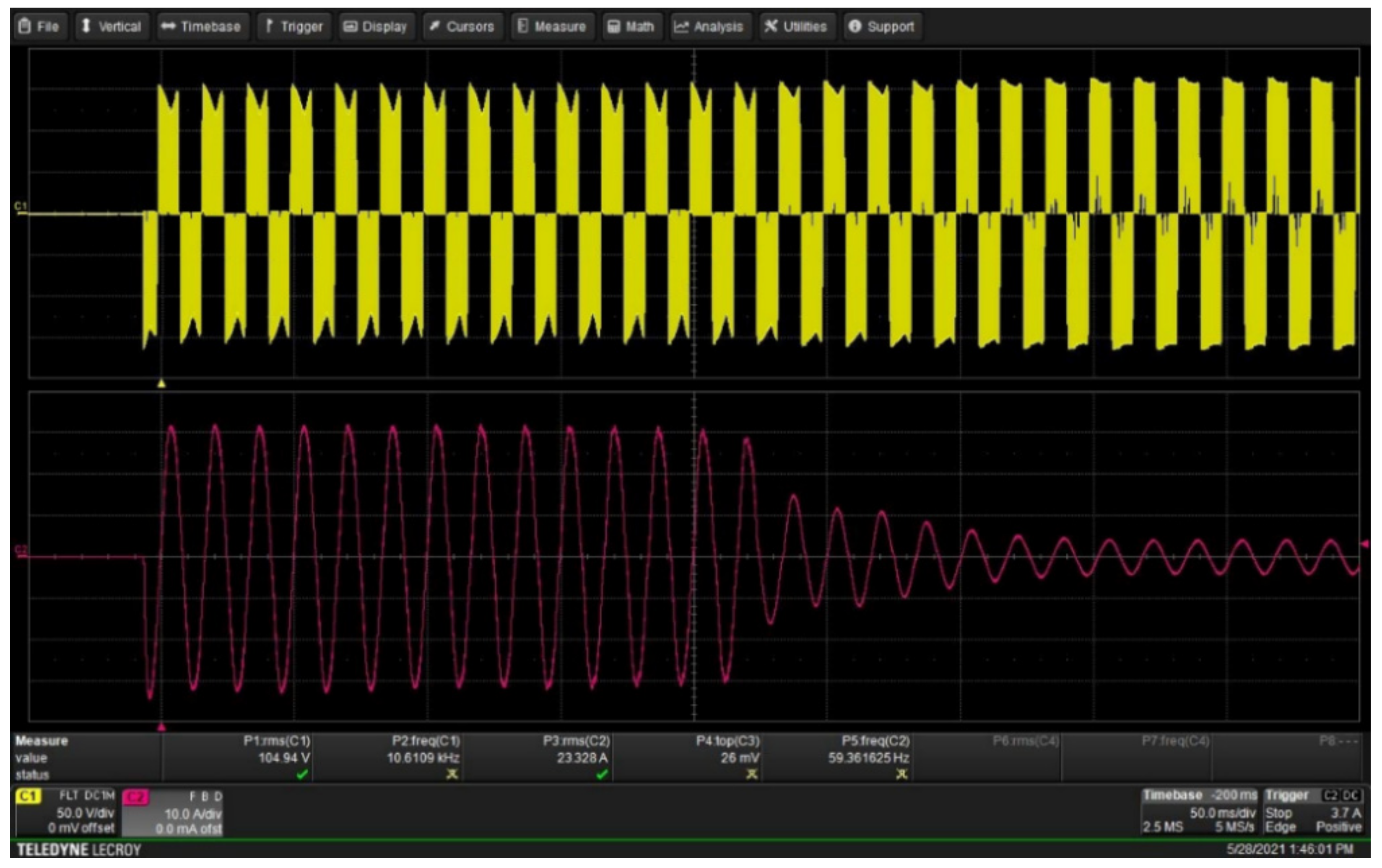
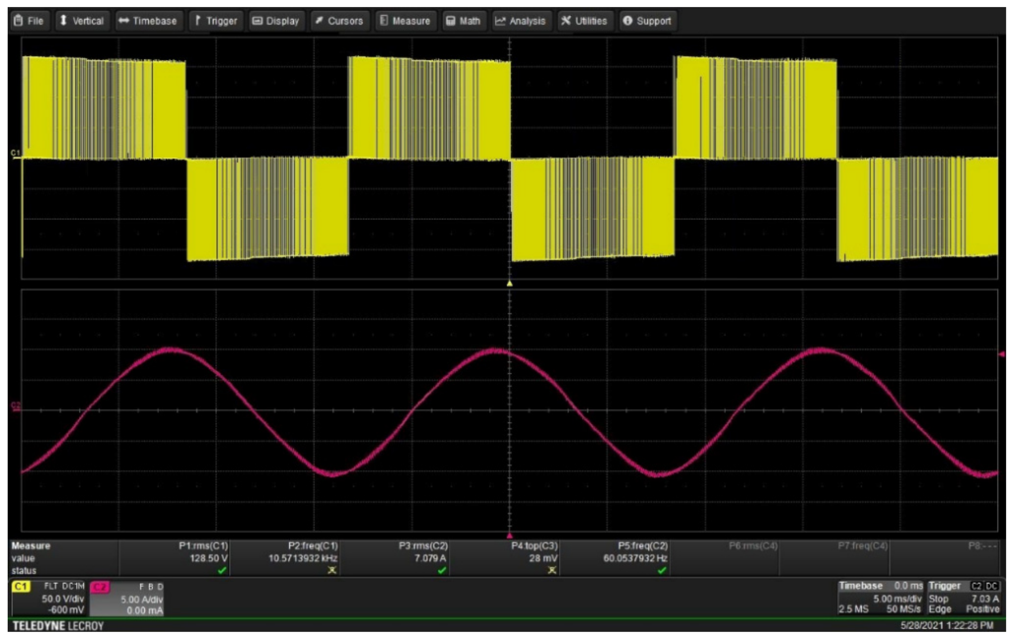
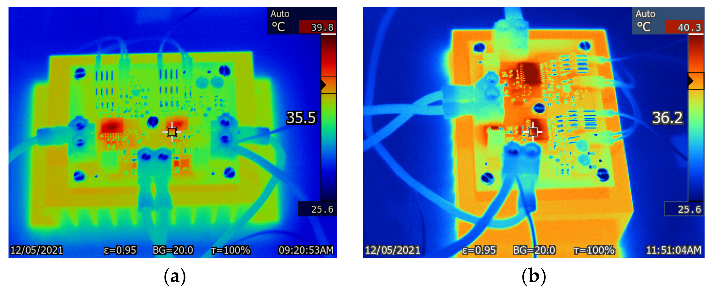
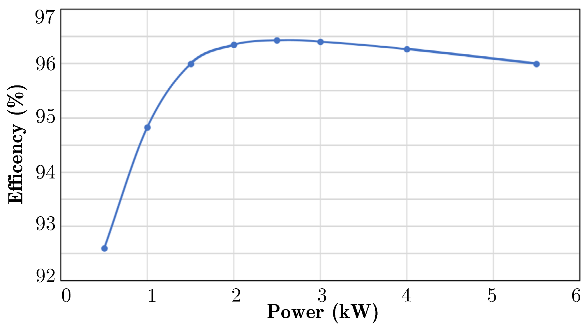
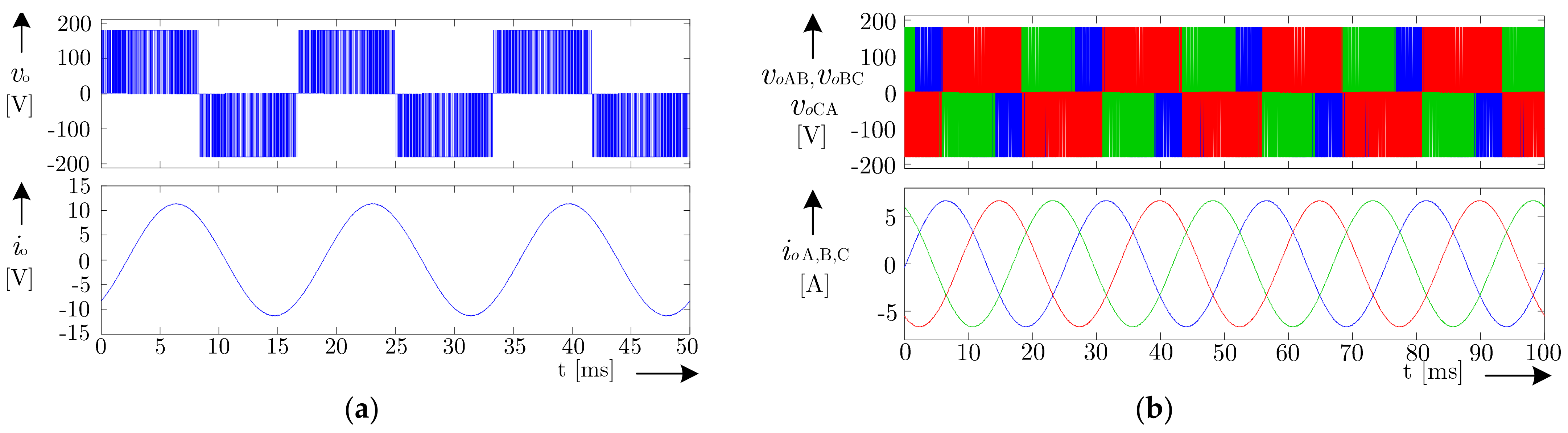
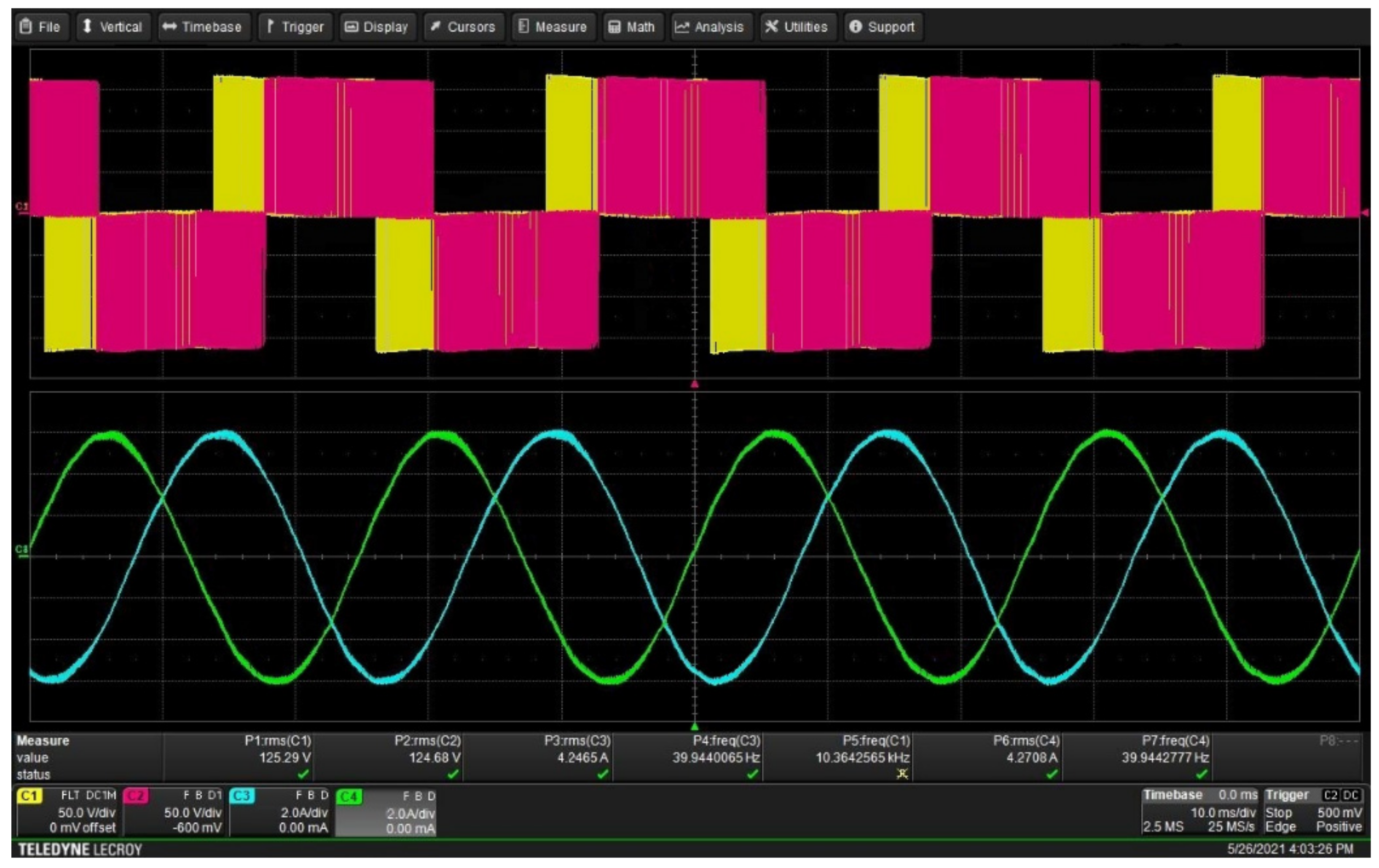
High current traces often cause EMI. They can be reduced by placing ground planes on both side of the traces and on opposite sides of the PCB, thus effectively enclosing the high current traces with ground. The large ground conductor areas behave as electrostatic shields, trapping the radiated energy in the form of eddy currents, which dissipate as heat. Ground planes can sometimes consist of a single section of the electronic board. In other cases, when possible, they can occupy a complete copper layer. In addition, the length of the tracks should be as short as possible to reduce their parasitic effects [39].
The traces layout dimensions must be chosen according to the amount of current that the PCB must tolerate and the temperature that the circuit must withstand. Calculations can be made in accordance with the IPC-2221 standard. On the other hand, standards explain where and how to place the components on the board. The standard explains that the higher frequency components must be placed close to the power supply section, in order to have a shorter return to ground and thus avoid harmonic contamination.
It should be noted that the separation between components is due to the voltage level that they handle. In this way, circuits that are powered by voltages less than 15 V must be separated by 0.1 mm, while circuits with voltages greater than 180 V must be separated by 1.25 mm. This applies to the connecting tracks; however, it is also useful as a component measure, as distances less than these voltage levels can present an arc flash hazard.
Modern VSIs have experienced an increase in frequency, power, and control circuits. This means that the di/dt also increases. Therefore, in PCBs where a current flows with high rates of change, an induced voltage can be measured even when there are no conductors registered as spiral. This happens due to the value di/dt and not directly due to the value of the inductance since any electrical conductor has an intrinsic inductance. Therefore, with inductance values on the order of peak or nano Henries, it can still measure voltages that, depending on the frequency, could reach units of tens or even hundreds of volts. The value of stray inductances can be estimated with a certain degree of precision using mathematical formulas [40]. Stray inductances in electronic designs are due to the tracks on the PCB, so the connections between the components should be as short as possible. The easiest way to solve these unwanted effects involves reducing the operating frequency, which is not the best solution. A second way utilizes the reduction of the distance in the connection of the components. The greater the distance between connection points, the higher the parasitic inductive effect of the tracks. The greater the area of proximity to the ground planes of the board, the greater the parasitic capacitive effect.
There are two power input sections to control and drive the transistors. The source inputs have filter capacitors and protections circuits against over voltage, over current and reverse voltage. It is convenient to have these protections to create a system more robustly defended against the most common sources of failure. The 15 V input is designed with bigger capacitors because this circuit demands more instantaneous current, especially when driving the IGBT through the gate resistances.
Once all the components have been selected and the schematic diagrams are designed, the tracks of all the physical layers of the PCB are generated. It is important to follow a PCB design methodology, to determine and define design concepts. While designing, ease of assembly must be constantly reviewed to avoid creating a board that could be difficult or expensive to produce, either when protypes are manufactured or when mass production is carried out. The use of a CAD tool during PCB design is highly recommended, as it provides the possibility of verifying the description before implementation, reducing the cost of manufacturing [41]. With the help of the CAD tool, the circuit diagrams can be converted into a 3-dimensional (3D) image of the PCB, as shown in Figure 11a,b, to verify the design of the board prior to manufacture. Figure 11c,d show the implemented prototype of an HB power cell (top view and bottom view respectively). It is worth mentioning that the PCB was manufactured by a company dedicated to the subject, but it was welded in the laboratory of our institution. During the assembly, tests were carried out to ensure correct operation.

5.2. Results

In order to have previous references to compare voltage and current waveforms at the outputs of the single-phase and three-phase inverters, open loop control simulations were carried out, with DC-link voltage and loads similar to those that will be used in laboratory tests. Figure 12a shows simulated waveforms of vo and io at the output of the single-phase FB VSI in steady state. In this case, the unipolar SPWM technique was programmed with m = 0.85, fSW = 10 kHz and fo = 60 Hz. Figure 12b shows simulated results of the line voltages voAB, voBC and voCA, and of the three load currents ioA, ioB and ioC at the output of the three-phase VSI in steady state. In this case a three-phase SPWM technique was programmed with m = 0.85, fSW = 10 kHz and fo = 40 Hz.
To validate the developed HB cell prototype, some HB cells were manufactured to assemble VSIs in a modular way. To control the power cells, an STM32 nucleo-64 board with STM32F103RB microcontroller was used to implement the SPWM techniques [42]. It is well known that there are different modulation and closed-loop control techniques to obtain high-quality voltage and current waveforms at the output of the VSIs, however, it was not an objective of this work to implement advanced control techniques.
First, the single-phase FB inverter was assembled and tested using two HB cells. In this case, a single-phase unipolar SPWM technique was implemented in the microcontroller with the same parameters used for simulation.
Figure 13 shows a photograph of the experimental setup. For the case of the single- phase FB VSI, only two cells were used, but for the three-phase VSI test, the three power cells were used.
Figure 14 shows vo and io measurements at the output of the single-phase FB inverter during the run-up of a 1 HP single-phase split phase motor. We observed that, at the beginning, the load current reached a peak value of 33 A which is about 95% of the maximum design current of the HB power cell. The IGBTs can operate at a higher load; however, load current and the switching frequency were limited to keep power losses low.
Figure 15 shows vo and io measurements at the output of the same single-phase modular inverter, when the AC motor is fully loaded and in steady-state operation. It can be seen that the experimental results matched the results obtained through simulation. It should be mentioned that an adequate hardware design with its correct implementation and the dead-time compensation were key; the current ripple remained low and with a THD of approximately 2.5%, which is within the guidelines recommended by the IEEE Std. 519-2014 for interconnection to the electrical grid [43].
Figure 16 shows vo and io measurements at the output of the three-phase VSI, in steady state. The three-phase SPWM technique was programmed with m = 0.85, fSW = 10 kHz and fo = 40 Hz. For this test, a three-phase 3 HP induction motor was fed, which was softly started from low voltage and frequency. Again, the experimental results were very similar to the simulated ones, and the load currents also showed a low ripple.
Today, there are numerous closed-loop control techniques for single-phase and three-phase VSIs, which are used to build high-quality voltages and currents at the output, even under non-linear loads. The quality of the voltages and currents at the output of the VSI will ultimately depend on the type of electrical load and the type of control to be implemented [44].
The main requirements for high-performance VSIs generally are [45]: (1) low THD of voltages and currents at the output, (2) quick transient response in case of sudden load change, and (3) steady-state errors kept as small as possible.
Temperature measurements were made with a Fluke Ti32 industrial thermal imager to evaluate the thermal performance of the HB cell. The thermal graph of an HB cell after operating for 30 min (to bring the package’s temperature rise to equilibrium) with 50% of the nominal load is shown in Figure 17a, and the thermal image after three hours under the same load condition is shown in Figure 17b. We noted that, without active cooling, the hottest spots were the GDs, the gate resistors, and the snubber circuits. According to the GD’s technical datasheet (see Table 2), and considering the temperature difference observed in Figure 17b, the dissipated power by each GD is PD = 241.102 mW.
Finally, Figure 18 shows the electric efficiency measurement of the single-phase FB inverter, which was carried out with a BK Precision power meter 5335B. The maximum power efficiency in this test (180 V in DC-link) was 96.4% at 2.5 kW.
The European efficiency value was evaluated at 95.2%, which is within the mean for single-phase FB VSIs according to their respective trend lines [22].

6. Conclusions

In this work, the development of an IGBT-based HB cell to assemble VSIs of different topologies in a modular way was presented. The HB cell was designed in accordance with local and international standards while considering a low-cost and high-performance design, especially for home and laboratory applications.
To reach the design requirements of low power consumption and reduced EMI—and achieve a high conversion efficiency board—during the PCB design process, mainly surface-mounted components were used, allowing for a reduced board size. Those same design choices also allowed the tracks between components to be kept very short. Snubber circuits were implemented to reduce the voltage spikes that appear when the IGBTs are turned off. This, together with the compensation of the dead-time effect, meant that the current presented a low ripple, which will allow the developed HB cell to be useful and approved for grid interconnection.
The prototype’s performance, efficiency, and thermal analysis were validated and experimentally tested with single-phase and three-phase VSI topologies, and the experimental results showed a high level of efficiency with the proposed design. Of course, the quality of the voltage and current waveforms at the output of the VSIs can be increased by using state-of-the-art closed-loop control strategies and advanced techniques to generate gating signals.
The developed power cell is very suitable for the assembly of MLIs that can be used to control the generated energy from renewable sources, but in that case, special attention must be paid to the parallel operation of each cell—and on its DC-link side. The assembly of MLIs of different levels and their control techniques will be the next research topics undertaken.

Author Contributions

Conceptualization, R.M.-C. and J.F.P.-C.; methodology, R.M.-C. and J.F.P.-C.; software, J.F.P.-C.; validation, R.M.-C.; investigation, R.M.-C. resources, H.P.M.-H. and R.C.-M.; writing—original draft preparation, R.M.-C.; project administration, R.C.-M. and H.P.M.-H. All authors have read and agreed to the published version of the manuscript.

Funding

This research was funded by Tecnológico Nacional de México, Project No. 10609.21-P.

Conflicts of Interest

The authors declare no conflict of interest.

Abbreviations

ACAlternating current
ADAutomated design
CADComputer-aided design
DCDirect current
DFRDesign for reliability
EMIElectromagnetic interference
FBFull bridge
GaN-IGBTGallium nitride insulated-gate bipolar transistor
GDGate driver
GNDGround
HBHalf-bridge
HPHorsepower
IGBTInsulated-gate bipolar transistor
IPCInstitute of printed circuits
MLIMultilevel inverters
MODOMulti objective design optimization
MOSFETMetal-oxide-semiconductor field-effect transistor
NOMOfficial Mexican standards
PCBPrinted circuit board
PSSPower semiconductor switch
rmsRoot mean square
siC-IGBTSilicon carbide insulated-gate bipolar transistor
SPWMSinusoidal Pulse-width modulation
TDTraditional design
THDTotal harmonic distortion
VSIVoltage-source inverter

References

  1. Trzynadlowski, A.M. Introduction to Modern Power Electronics, 2nd ed.; Wiley: Hoboken, NJ, USA, 2010; pp. 269–3086. [Google Scholar]
  2. Rashid, M.H. Power Electronics Handbook. In Devices, Circuits, and Applications, 3rd ed.; Elsevier: Pensacola, FL, USA, 2015; pp. 357–360. [Google Scholar]
  3. Kolar, J.W. Power electronic design 4.0. In In Proceedings of the Workshop at the ECPE Design Automation Expert Discussion, Zurich, Switzerland, 19 July 2019. [Google Scholar]
  4. Marques Cardoso, A.J. Power electronics design methods and automation in the digital era: Evolution of design automation tools. IEEE Power Electron. Mag. 2020, 7, 36–40. [Google Scholar] [CrossRef]
  5. Nami, A.; Liang, J.; Dijkhuizen, F.; Demetriades, G.D. Modular multilevel converters for HVDC applications: Review on converter cells and functionalities. IEEE Trans. Power Electron. 2015, 30, 18–36. [Google Scholar] [CrossRef]
  6. Perez. M.A.; Steffen, B.; Rodriguez, R.; Kouro, S.; Lizana, R. Circuit topologies, modeling, control schemes, and applications of modular multilevel converters. IEEE Trans. Power Electron. 2015, 30, 4–17. [Google Scholar] [CrossRef]
  7. Hassan, A.; Yang, X.; Che, W.; Houran, M.A. A state of the art of the multilevel inverters with reduced count components. Electronics 2020, 9, 1924. [Google Scholar] [CrossRef]
  8. Buttay, C.; Martin, C.; Morel, F.; Caillaud, R.; Le Leslé, J.; Mrad, R.; Degrenne, N.; Mollov, S. Application of the PCB-embedding technology in power electronics–state of the art and proposed development. In Proceedings of the Second International Symposium on 3D Power Electronics Integration and Manufacturing (3D-PEIM), College Park, MD, USA, 25–27 June 2018; pp. 1–10. [Google Scholar]
  9. Software Engineering Center (IPA/SEC). ESPR Embedded System Development Process. Reference Guide, version 2.0; Information-Technology Promotion Agency: Tokyo, Japan, 2012; pp. 217–227. [Google Scholar]
  10. Nawawi, A.; Tong, C.F.; Yin, F.; Sakanova, A.; Liu, Y.; Liu, Y.; Kai, M.; See, K.Y.; Tseng, K.-J.; Simanjorang, R.; et al. Design and demonstration of high power density inverter for aircraft applications. IEEE Trans. Ind. Appl. 2017, 53, 1168–1176. [Google Scholar] [CrossRef]
  11. Lu, H.; Bailey, C.; Yin, C. Design for reliability of power electronics. Microelectron. Reliab. 2009, 49, 1250–1255. [Google Scholar] [CrossRef]
  12. Wang, H.; Ma, K.; Blaabjerg, F. Design for reliability of power electronic systems. In Proceedings of the 38th Annual Conference IEEE Industrial Electronics Society, Montreal, QC, Canada, 25–28 October 2012; pp. 33–44. [Google Scholar]
  13. Wang, H.; Liserre, M.; Blaabjerg, F.; Rimmen, P.P.; Jacobsen, J.B.; Kvisgaard, T.; Landkildehus, J. Transitioning to physics-of-failure as a reliability driver in power electronics. IEEE Trans. Emerg. Sel. Top. Power Electron. 2014, 2, 97–114. [Google Scholar] [CrossRef]
  14. Raggl, K.; Nussbaumer, T.; Doerig, G.; Biela, J.; Kolar, J.W. Comprehensive design and optimization of a high-power-density single-phase boost PFC. IEEE Trans. Ind. Electron. 2009, 56, 2574–2587. [Google Scholar] [CrossRef]
  15. Kolar, L.W.; Biela, J.; Waffler, S.; Friedli, T.; Badstuebner, U. Performance trends and limitations of power electronic systems. In Proceedings of the 6th International Conference on Integrated Power Electronics Systems, Nuremberg, Germany, 16–18 March 2010; pp. 1–20. [Google Scholar]
  16. Burkart, R.M. Advanced Modeling and Multi-Objective Optimization of Power Electronic Converter Systems. Ph.D. Thesis, ETH, Zurich, Switzerland, 2016. [Google Scholar]
  17. Mehrabadi, N.R. Power Electronics Design Methodologies with Parametric and Model-Form Uncertainty Quantification. Ph.D. Thesis, Virginia Polytechnic Institute and State University, Blacksburg, VA, USA, 2018. [Google Scholar]
  18. Bindra, A.; Mantooth, A. Modern tool limitations in design automation: Advancing automation in design tools is gathering momentum. IEEE Power Electron. Mag. 2019, 6, 28–33. [Google Scholar] [CrossRef]
  19. Voldoire, A.; Schanen, J.-L.; Ferrieux, J.-P.; Derbey, A.; Gautier, C. Three-phase PWM voltage-source-inverter weight optimization for aircraft application using deterministic algorithm. Electronics 2020, 9, 1393. [Google Scholar] [CrossRef]
  20. Andreta, A.; Lavado Villa, L.; Lembeye, Y.; Crebier, J.C. A novel automated design methodology for power electronics converters. Electronics 2021, 10, 271. [Google Scholar] [CrossRef]
  21. Bughneda, A.; Salem, M.; Richelli, A.; Ishak, D.; Alatai, S. Review of multilevel inverters for PV energy system applications. Energies 2021, 14, 1585. [Google Scholar] [CrossRef]
  22. Araujo, S.V.; Zacharias, P.; Mallwitz, R. Highly efficient single-phase transformerless inverters for grid-connected photovoltaic systems. IEEE Trans. Ind. Electron. 2010, 57, 3118–3128. [Google Scholar] [CrossRef]
  23. Renken, F. The dc-link capacitor current in pulsed single-phase H-bridge inverters. In Proceedings of the EPE Conference, Dresden, Germany, 11–14 September 2005; Volume 10, pp. 1–10. [Google Scholar]
  24. Vujacic, M.; Hammami, M.; Srndovic, M.; Grandi, G. Theoretical and experimental investigation of switching ripple in the DC-link voltage of single-phase H-bridge PWM Inverters. Energies 2017, 10, 1189. [Google Scholar] [CrossRef]
  25. Chen, T.; Li, S.; Fahimi, B. Analysis of dc-link voltage ripple in voltage source inverters without electrolytic capacitor. In Proceedings of the IECON Conference, Washington, DC, USA, 20–23 October 2018; pp. 1–8. [Google Scholar]
  26. Blake, C.; Bull, C. IGBT or MOSFET: Choose Wisely; Data Sheet No. PD60147; International Rectifier: El Segundo, CA, USA, 2005. [Google Scholar]
  27. Dodge, J.; Hess, J. Advanced Power Technology, Application Note APT0201-IGBT Tutorial. Available online: https://www.microsemi.com/document-portal/doc_view/14696-igbt-tutorial (accessed on 6 August 2021).
  28. Silicon Labs. An1009: Driving MOSFET and IGBT Switches Using the Si828x. Available online: https://www.skyworksinc.com/-/media/Skyworks/SL/documents/public/application-notes/AN1009-driving-mosfet-and-igbt-switches-using-the-si828x.pdf (accessed on 15 August 2021).
  29. Lobsiger, Y. Closed-Loop IGBT Gate Drive and Current Balancing Concepts. Ph.D. Thesis, ETH, Zurich, Switzerland, 2014. [Google Scholar]
  30. Fuji Electric Co. Ltd. Chapter 7 Gate drive circuit design. In Catalog Product Specifications; Fuji Electric Co: Offenbach, Germany, 2016. [Google Scholar]
  31. Skyworks. Si8285/86: Data Sheet. Available online: https://www.skyworksinc.com/-/media/SkyWorks/SL/documents/public/data-sheets/si8285-86-data-sheet.pdf#unique_8_fig_z55_jqw_m5 (accessed on 5 May 2021).
  32. Skyworks. AN486: High-Side Bootstrap Design Using ISO Drivers in Power Delivery Systems; Skyworks: Irvine, CA, USA, 2021. [Google Scholar]
  33. Mora, A.; Juliet, J.; Santander, A.; Lezana, P. Dead-time and semiconductor voltage drop compensation for cascaded H-bridge converters. IEEE Trans. Ind. Electron. 2016, 63, 7833–7842. [Google Scholar] [CrossRef]
  34. Yamashita, Y.; Furuta, J.; Inamori, S.; Kobayashi, K. Design of RCD snubber considering wiring inductance for MHz-switching of SiC-MOSFET. In Proceedings of the 18th IEEE Workshop on Computers in Power Electronics, Stanford, CA, USA, 9–12 July 2017; pp. 1–6. [Google Scholar]
  35. Lee, S. How to Select a Heat Sink. Available online: https://www.electronics-cooling.com/1995/06/how-to-select-a-heat-sink/ (accessed on 9 August 2021).
  36. Künzi, R. Thermal Design of Power Electronics Circuits; CERN Yellow Report CERN-2015-003; CERN: Baden, Switzerland, 2014; pp. 1–7. [Google Scholar]
  37. IPC. Homepage. Available online: https://www.ipc.org/ (accessed on 7 June 2021).
  38. Binz, R.; Bracho, R.; Anderson, A.; Coddington, M.H.; Hale, E.T.; Ingram, M.; Martin, M.; Mendoza, C.I.; Normark, B.; Olofsson, M.; et al. A Report on the Implementation of Smart Grids in Mexico NREL/TP-7A40-72699; National Renewable Energy Laboratory: Golden, CO, USA, 2019; pp. 1–128. [Google Scholar]
  39. Chentian, Z. EMC in Power Electronics and PCB Design. Ph.D. Thesis, Clemson University, Clemson, SC, USA, 2014. [Google Scholar]
  40. Bondarenko, N. Electromagnetic Compatibility in Power Inverter Design. Ph.D. Thesis, Missouri University of Science and Technology, Rolla, MO, USA, 2015. [Google Scholar]
  41. Morales-Caporal, R.; Reyes-Galaviz, A.S.; Casco-Vásquez, J.F.; Martínez-Hernández, H.P. Development and implementation of a relay switch based on WiFi technology. In Proceedings of the International Conference on Electrical Engineering, Computing Science and Automatic Control (CCE), Mexico City, Mexico, 11–13 November 2020; pp. 1–6. [Google Scholar]
  42. STMicroelectronics. PWM Resolution Enhancement Through a Dithering Technique for STM32 Advanced-Configuration, General-Purpose and Lite Timers Application Note AN4507; STMicroelectronics: Geneva, Switzerland, 2017; pp. 1–22. [Google Scholar]
  43. IEEE Power and Energy Society. Recommended practice and requirements for harmonic control in Electric power systems. In Proceedings of the IEEE Std 519-2014 (Revision of IEEE Std 519-1992), Piscataway, NJ, USA, 11 June 2014; pp. 1–29. [Google Scholar]
  44. Mercorelli, P.; Kubasiak, N.; Liu, S. Multilevel bridge governor by using model predictive control in wavelet packets for tracking trajectories. In Proceedings of the IEEE International Conference on Robotics and Automation (ICRA), New Orleans, LA, USA, 26 April–1 May 2004; pp. 4079–4084. [Google Scholar]
  45. Chang, E.-C.; Cheng, C.-A.; Wu, R.-C. Robust optimal tracking control of a full-bridge DC-AC converter. Appl. Sci. 2021, 11, 1211. [Google Scholar]
Figure 1. The most common power cells and their voltage levels: (a) HB cell; (b) FB cell.
Electronics 10 02549 g001
Figure 2. Power inverter traditional design flow.
Electronics 10 02549 g002
Figure 3. Reliability design procedure for power electronics.
Electronics 10 02549 g003
Figure 4. Power electronics performance trends: (a) achievable performance using state-of-the-art technology (blue) and performance limits due to physical barriers (red), (b) improvements over time, (c) expected performance (green).
Electronics 10 02549 g004
Figure 5. Simplified workflow of the virtual prototyping routine of the MODO-based process.
Electronics 10 02549 g005
Figure 6. Simplified workflow of the AD method.
Electronics 10 02549 g006
Figure 7. HB cell with basic push-pull resistive gate drives and parasitic capacitances of the IGBTs.
Electronics 10 02549 g007
Figure 8. (a) Desaturation circuit; (b) Bootstrap.
Electronics 10 02549 g008
Figure 9. Discharge-suppressing RCD snubber circuit.
Electronics 10 02549 g009
Figure 10. (a) IGBT+diode on the heat sink; (b) thermal resistance circuit and (c) parameters of the thermal circuit.
Electronics 10 02549 g010
Figure 11. Developed HB cell: (a) 3D model, top view; (b) 3D model, bottom view; (c) implemented prototype, top view; (d) implemented prototype, bottom view.
Electronics 10 02549 g011
Figure 12. Simulated results of voltage and load current at the output of the inverter with open loop SPWM and in steady state; (a) single-phase FB VSI; (b) three-phase VSI.
Electronics 10 02549 g012
Figure 13. Photograph of the experimental setup.
Electronics 10 02549 g013
Figure 14. Experimental results of voltage and current at the output of the modular single-phase FB VSI, in dynamic state (50 V/div, 10 A/div, 50 ms/div).
Electronics 10 02549 g014
Figure 15. Experimental results of voltage and current at the output of the modular single-phase VSI, steady state (50 V/div, 5 A/div, 5 ms/div).
Electronics 10 02549 g015
Figure 16. Experimental results of voltage and current at the output of the modular three-phase VSI, steady state (50 V/div, 2 A/div, 10 ms/div).
Electronics 10 02549 g016
Figure 17. Temperature distribution of an HB cell with 50% of the nominal load: (a) after 30 min of operation; (b) after 3 h of operation.
Electronics 10 02549 g017
Figure 18. Efficiency curve of the power stage of a FB VSI for an input voltage of 180 V in DC-link.
Electronics 10 02549 g018
Table 1. Specifications of the FB power cell.
NameSymbolValue
Grid phase voltage (rms)vs120 V ± 10%
DC-link voltageVdc50–180 V
Grid frequencyfs60 Hz
Inverter maximal output currentIo35 A
Maximum output powerPm6 kW
Inverter output frequencyfo0–60 Hz
Inverter switching frequencyfSW10 kHz
Table 2. The main electronic components of the HB cell board.
SymbolDatasheet ValuesCalculated ValuesUnits
IGBT APT80GA60LD40 (Vce = 600 V, Ic = 75 A at TC = 100 °C)
Q total , QG230, 78 nC
Cies = [CGE + CGC], Coes = [CGC + CCE], Cres = CGC6390, 580, 63 pF
td(on), td(off), trise, tfall23, 158, 31, 132 ns
RθJC (IGBT), RθJC (diode)0.2, 0.67 °C/W
PD625 (TC = 25 °C)259.740 (TC = 100 °C)W
TJ, TSTG−55 to 150 °C
Isolated Gate Driver si8285
Common Mode Transient Immunity12525MAXkV/µs
VDDA, VDDB, −VSSB3.0–5.5, 10.0–30.0, 10.0–30.0 V
R0G,on, R0G,off, RDSAT2.48, 0.86, 100
RG,on, RG,off0–10, 0–10 (VDDB = 15 V)10, 8.2
DDSAT
D1
DBOOT
D2
ES1J for 600 V
-
-
-
STTH112A for 1200 V MMSZ5242BS-7-F for 12 V,
STTH2L06UFY for 600 V
MM3Z16VT1G for 16 V
CBL, CBOOT390, -0.22, 1µF
iG iG,on 2.8, iG,off 3.4 (VDDB = 15 V)A
PD410 (when TJTA = 25 °C)245.9 (when TJTA = 15 °C)mW
TJ, TA150MAX, −40 to 125100, 25°C
Table 3. Snubber circuit parameters.
NameSymbolCalculated ValueSelected Value by Tests
Total parasitic inductance of the circuitLs-687.835 nH
Drain current at turn-offIoff_MAX40 A-
Peak surge voltageVPS250 V-
Snubber capacitor (Film capacitor, 400 V)CSNUB224.60 nF150 nF
Snubber resistance (MELF, 500 V)RSNUB193.58 Ω150 Ω
Snubber Diode (Ultra-fast, 600 V)DSNUB-MURS260T3G
Publisher’s Note: MDPI stays neutral with regard to jurisdictional claims in published maps and institutional affiliations.

