Article

Step Coverage and Dry Etching Process Improvement of Amorphous Carbon Hard Mask

1
State Key Laboratory of ASIC and System, School of Microelectronics, Fudan University, Shanghai 200433, China
2
National Integrated Circuit Innovation Center, Shanghai 201203, China
*
Author to whom correspondence should be addressed.
Electronics 2021, 10(20), 2512; https://doi.org/10.3390/electronics10202512
Submission received: 6 September 2021 / Revised: 9 October 2021 / Accepted: 12 October 2021 / Published: 15 October 2021
(This article belongs to the Section Semiconductor Devices)

Abstract

:
Amorphous carbon hard mask (ACHM) films have been widely applied as protective components and hard etching masks in lithography and dry etching processes. The capability of lithography is directly dependent on the step coverage (SC) of the ACHM. Poor SC may impact the protection of device patterns during the etching process and lead to overlay marks occurring in lithography. In this work, the ACHM film processing process is engineered and optimized towards better SC through the comparative study of the C2H2 and C3H6 precursors at different temperatures. Furthermore, a process parameter design of experiment (DOE), with C2H2 as a precursor to optimize the dry etching rate, is proposed. The results of the experiment show that the dry etching performance is enhanced by higher power, temperature and C2H2 flow, and a smaller gap, lower pressure and lower carrier gas flow. A selective etching ratio of SiO2 and SiN, with an improved process window, is obtained. ACHM film elimination process is also validated by characterizing the surface roughness. The demonstrated results can be instructive in terms of the optimization of etching process in future semiconductor manufacturing.

1. Introduction

For the scaling of the critical sizes of semiconductor devices down to sub-100 nm, advanced hard mask films, with superior performance to those of conventional polymer resistors, are required [1,2,3]. With the emergence of new technologies and structures, such as double patterning and high aspect ratio patterns, lithographic and etching processes are becoming more difficult and less popular due to their use of thin photoresistors [4]. Hence, the bending or wiggling of the patterns can easily occur. For the passivation layer in memory or logic devices, as shown in Figure 1, one of the key challenges relates to obtaining a hard mask (HM) with better step coverage (SC) and a higher selective etching ratio in lithographic and dry etching processes, which is important due to special requirements of stacked layers and easier elimination to ensure good surface roughness. The amorphous carbon hard mask (ACHM) has been applied to the fabrication of semiconductors, replacing the conventional SiO2 or Si3N4 hard mask due to its excellent physical properties and chemical stability. ACHM can be deposited using a variety of deposition methods, among which the plasma-enhanced chemical vapor deposition (PECVD) method has been widely used because of its high productivity, low cost, and tenability in terms of its film properties [5,6,7]. However, experimental studies focusing on the simultaneous optimization of the film step coverage and dry etching characteristics, using different parameters, have rarely been conducted and reported.
In this work, C2H2 and C3H6 reactant sources are employed to compare the sidewall and bottom SC at 200 °C and 400 °C, respectively. The etching rate performance with the C2H2 carbon source is further studied for different process parameters. An optimum deposition parameter of ACHMs with boosted selective etching ratios of SiO2 and SiN is experimentally studied. The ACHM elimination process can be also validated by characterizing the surface roughness after O2 the cleaning of plasma.

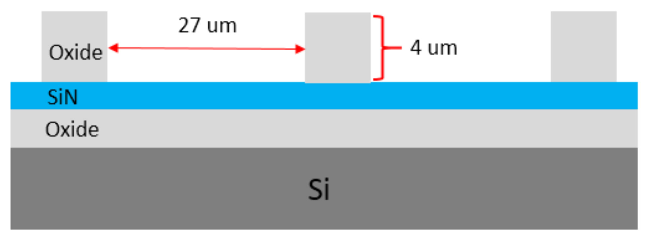
2. Materials and Methods
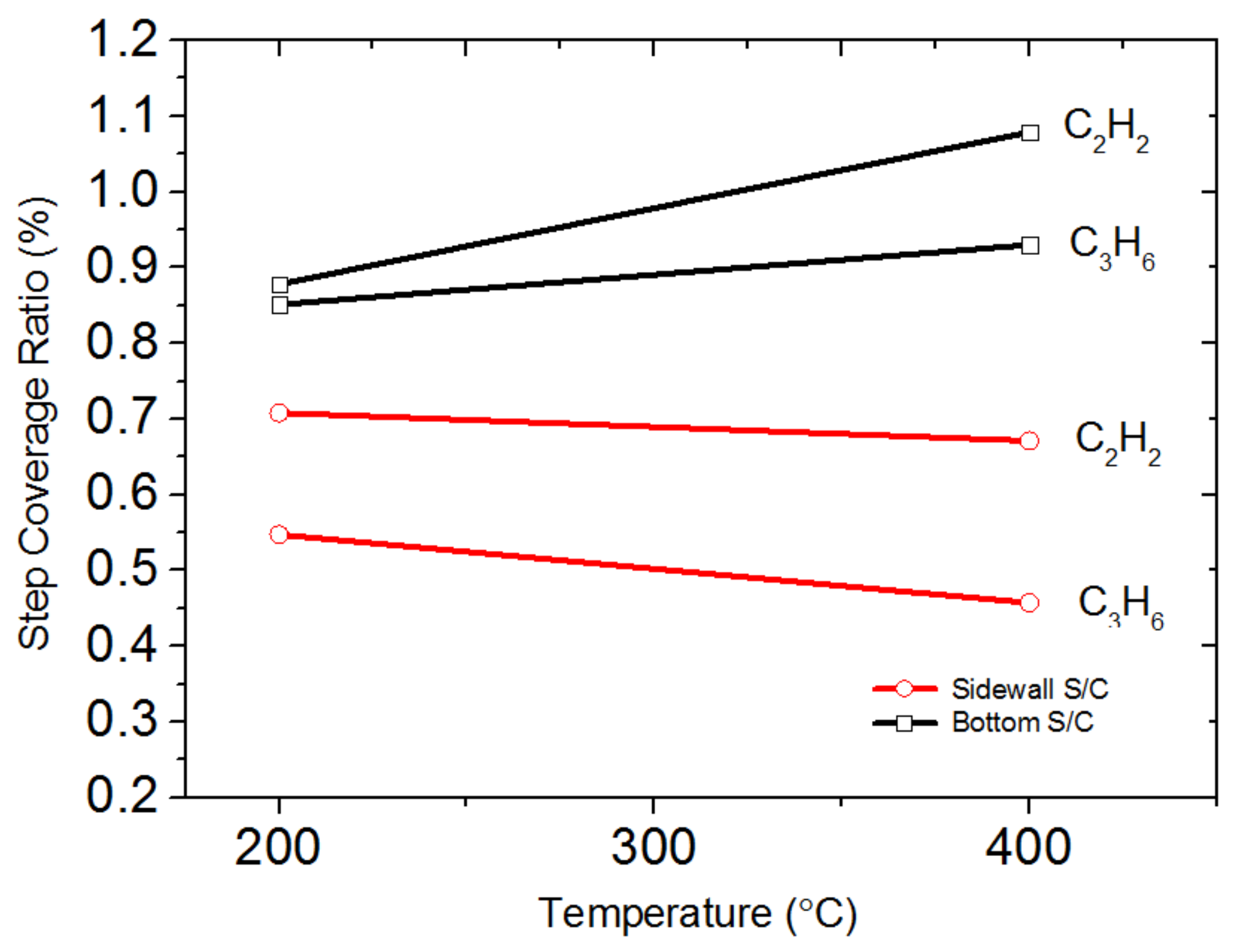
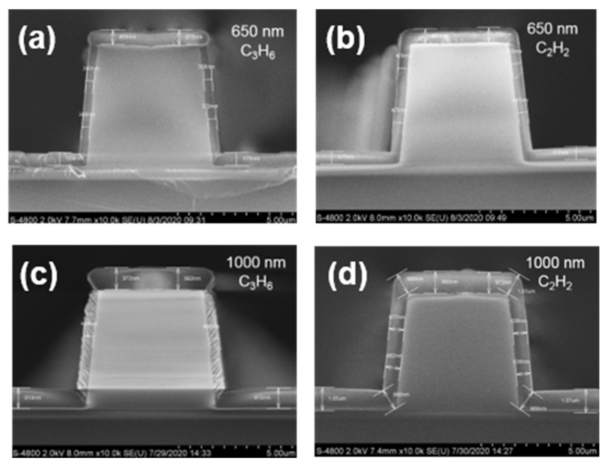
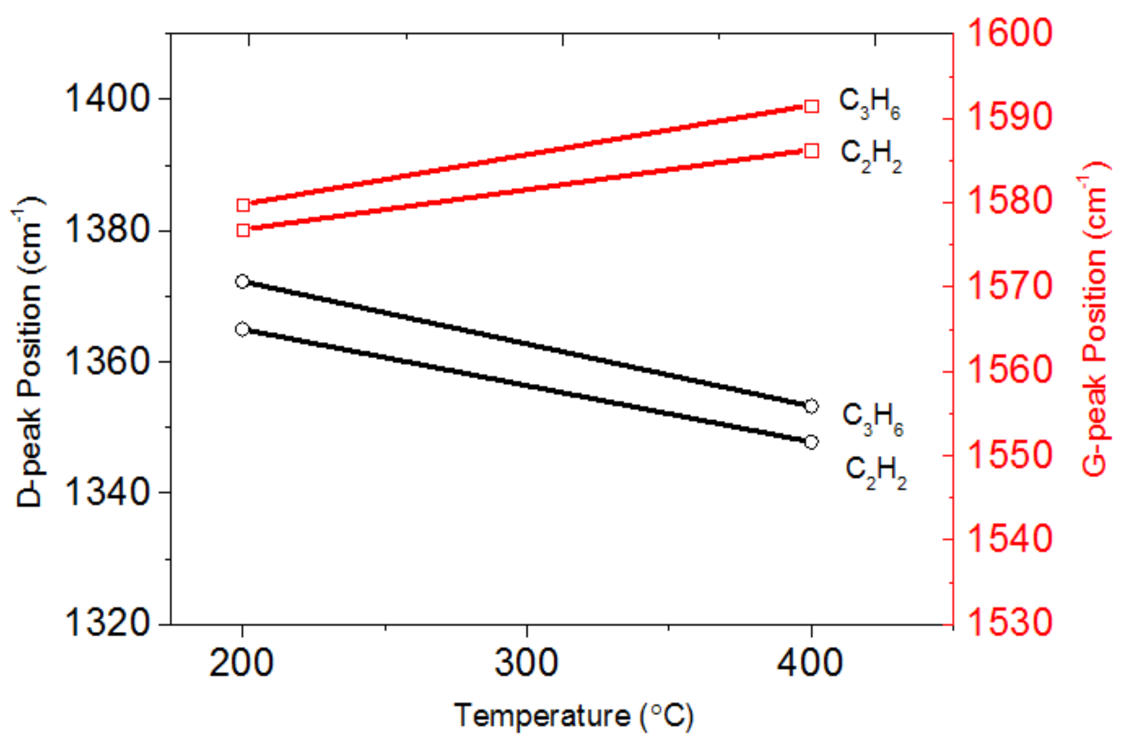
ACHM films with different thickness of 650 nm and 1000 nm were deposited on p-type Si substrates via the PECVD method, employing C2H2 and C3H6 as carbon sources. In detail, after the cleaning of wafers with diluted HF and SC1 solution, the wafers were loaded in the PECVD chamber for ACHM deposition with 550 W RF power. The flow rates of C2H2 and C3H6 were both 650 sccm, with a reactor pressure of 4 torr. Different deposition temperatures of 200 °C and 400 °C were used, and the SC ratio and film structure were characterized by cross sectional scanning electron microscopy (SEM).
One design of experiment (DOE) method was used and eight parameters of a C2H2-based ACHM process were investigated, as illustrated in Table 1. The experiment was conducted with high and low radio frequencies (HRF and LRF), power levels, temperatures, pressure levels, and gaps (the distances between the plasma and target wafer). C2H2 was the final precursor for ACHM, and Argon (Ar) and helium (He) were used as carrier gases of C2H2. The dry etching rates were measured by a Spectroscopic Ellipsometer, which was obtained from KLA-Tencor Aleris 8500. The chemical structure and C-H bonding were measured by Raman spectroscopy. The deposited film was etched using O2 plasma as well as a mixture of CF4 and CHF3. The film thickness was measured after each deposition and etching process, and the dry etching selectivity was further calculated. The surface roughness was measured using the Vicco Dimension-X AFM system.

3. Results

Figure 2 shows the SC ratio with different carbon sources and different levels of ACHM film thickness, measured by SEM, as a function of the deposition temperature. The sidewall and bottom SC exhibited similar trends for different carbon sources and thicknesses. For the 650 nm ACHM at a temperature of 200 °C, when using C2H2 to replace C3H6, the sidewall SC ratio was improved, increasing from 53.2% to 67.3%, and the bottom SC ratio was also increased from 85.1% to 87.8%. Similarly, for the 1000 nm ACHM at a temperature of 400 °C, the sidewall and bottom SC ratios were improved, increasing from 45.7% to 67.1%, and from 93.0% to 107.9%, respectively. Therefore, the thinner film had better sidewall SC; this was because the deposition rate became slower in the sidewall compared to the top and bottom for this pattern.
Figure 3 shows the cross-sectional SEM images of the SC performance obtained using C3H6 and C2H2 as carbon sources at 200 °C and 400 °C, with 650 nm and 1000 nm thickness, respectively. The SC performance observed using C2H2 for different temperatures and thicknesses showed a smoother profile than that observed when using C3H6 at the top, sidewall, corner and bottom locations. Furthermore, the film was discontinuous at the sidewall and corner at temperatures below 400 °C when using C3H6. However, for the C2H2 carbon source, the film showed not only continuous morphology but also better SC at the sidewall and corner.
The results obtained in this experiment theoretically confirm that the ratio of C/H in hydrocarbon species is strongly correlated with the sticking efficiency of the hydrogenated film reaction behaviors, and the sticking efficiency improves with the increasing of the C/H ratio [8,9]. Our experimental results further verify the theory that the C/H ratios obtained using C2H2 are higher than those obtained using C3H6. In addition, the ACHM obtained using the C2H2 precursor in this study also enabled superior SC performance in terms of the alignment and the overlay marks in the lithography process.
The transparent performance of the ACHM when using C2H2 was also better than that obtained with the C3H6 precursor. Figure 4 shows the Raman shift of the D and G-peaks with the increasing of the deposition temperature. With the increasing of the temperature from 200 °C to 400 °C, the position of the D and G-peaks, when using C2H2, shifted from 1365.01 to 1347.81 cm−1, and from 1576.81 to 1586.29 cm−1, respectively, while for ACHM, with the use of C3H6, the D and G-peaks shifted from 1372.27 to 1353.25 cm−1, and from 1579.81 to 1591.56 cm−1, respectively. Such a positive shift in the G-peak position was due to the increase in the size and number of sp2 bonding carbon clusters. The negative shift in the D-peak position suggests better transparency of the ACHM film [10].
From the above results, it can be concluded that the thinner ACHM film, when using C2H2, had better SC and transparency performance than that obtained when using C3H6. Such performance is critical for hard masks in lithography applications due to the direct impact on the yield data and process cost. Furthermore, the etching selectivity of ACHM as a hard etching mask is another important parameter in the etching process. An optimized design of experiment (DOE) was carried out to seek the key parameters of C2H2 as a precursor to improve the etching performance, as shown in Table 1.
As shown in Figure 5a, LRF could obtain a lower etching rate (ER) and higher HRF, and LRF power could also obtain a lower ER, which enabled improvements in the durability of etching. However, further increasing the HRF and LRF power did not provide an obvious improvement in the ER. In the plasma processing process, the injection of ion flux through the plasma sheath could be increased by the increased number of ions. LRF had a larger bias voltage, and as the power increased, the ions had sufficient energy to bake H and also to overcome to damage inflicted on the large graphitic sp2 structures, which resulted in dense film [11,12]. Higher power also enhanced the neutral and ion bombardment energy to the surface, which increased the building of sp3 structures. Therefore, these two parameters both brought greater benefits in terms of deceasing the etching rate during the etching process [13].
Figure 5b shows the dependence of ER on the temperature and the C2H2 flow rate. Lower ER was enabled by using higher temperatures and larger C2H2 gas flow rates. The ER improvement ratios, obtained by increasing the temperature and C2H2 flow, were about 14.2% and 9.8%, respectively. Under higher temperatures, it was easier for the hydrogen to bake out from the surface, which was more vulnerable to carbon ionic and radical chemisorption. As a result, the ACHM film became denser. The dependence of ER on the He and Ar flow rates was further studied. As shown in Figure 5c, the dependence on Ar and He carrier gases showed different behaviors, and lower ER was observed with higher Ar gas flow rates and also with lower He gas flow rates. This was the case because, in general, the total gas flow increases the Ar flow rate more significantly when the pressure and gap of the chamber remain constant. This will increase gas density, leading to more particle collisions. Therefore, the mean free path of the charged particles is reduced and the film density is improved. However, for He flow, charged He atoms can be easily pumped from the exhaust port due to the lower molecular weight, which will slightly lower the heat in the chamber, and thus, will dissipate the effect of film deposition and density [14,15]. Ar gas flow is a more sensitive parameter than He gas flow for ER optimization.
Figure 5d shows the relationship between ER and the pressure and gap, and a similar trend is observed for both parameters with a lowered ER under decreasing pressures and gaps. The ER was improved from 2263 Å/min to 1947 Å/min with the decreasing of the pressure from 6 torr to 4 torr. However, the ER was improved from 2268 Å/min to 1960 Å/min by decreasing the gap from 15 mm to 10 mm. The ER improvement ratios were 13.9% and 13.6% for the decreasing of the pressure and gap, respectively. The two parameters were both shown to be key parameters in terms of improving the etching durability of ACHM. According to the supplantation model, the pressure and the gap are utilized to determine the mean free path, and a lower pressure and gap would increase the ionic bombardment of the plasma, and thus, would improve the chemisorption of energetic carbonic ions [16,17]. As for pressure, such a phenomenon can be explained by the variation of the surface hydrogen coverage such that the adsorption and decomposition of the source molecules can react only at the region that does not have hydrogen atom coverage on the substrate [18]. Absorbed hydrogen atoms are produced by the decomposition of source molecules, and the density of the dangling bond sites where the source molecules can be adsorbed becomes smaller as the pressure becomes higher. Therefore, the ion bombardment energy will be increased in the low pressure to improve the count of sp2, which can be beneficial in terms of film hardness [19]. Therefore, ACHM film is improved with higher density and hardness.
Based on the above DOE results, optimized deposition process parameters could be obtained with improved dry etching selective ratios, which were 10.3 and 7.2 for SiO2 and SiN at 60 W bias power and 0.125 torr pressure in the etching system (Figure 6). Figure 6 a and b show the AFM images of the surface roughness before and after the obtaining of clean solutions for ACHM, with C2H2 as a carbon source, at 400 °C. The roughness RMS values of ACHM before and after cleaning were 1.17 nm and 1.66 nm, respectively, which indicates that the ACHM was effectively eliminated and that the surface roughness was adequate for memory device applications due to the effective suppression of the scattering of incident lasers during the lithography process.

4. Conclusions

From the demonstrated experimental results, it can be seen that the SC of ACHM film properties were optimized as a result of the different temperatures and precursors used in the PECVD deposition process. With the use of higher C/H ratios for the thinner C2H2-based ACHM film, an improvement in SC was achieved as compared to the C3H6-based ACHM. The optimization of the etching rate performance by means of DOE, with the goal of attaining high-reliability film quality, was further studied. Based on the DOE results and analysis, it can be concluded that the dry etching rate was enhanced by higher power, temperature and C2H2 flow, and lower pressure, smaller gaps and reduced carrier gas flow. The optimized process condition was achieved with dry etching selective ratios of 10.3 and 7.2 for SiO2 and SiN, respectively. The effective ACHM film elimination that was achieved in this study also provides a good basis for lithography processes involving with smooth surfaces. Our results show great potential for applications involving dry etching using hard masks in the fabrication of advanced semiconductor devices.

Author Contributions

Investigation, Z.J.; Resources, Q.S.; Supervision, D.Z.; Writing—review and editing, H.Z. All authors have read and agreed to the published version of the manuscript.

Funding

This work was supported by the National Key Research and Development Program of China (2017ZX02315005) and the Support Plans for the Youth Top-Notch Talents of China.

Data Availability Statement

The data presented in this study are available on request from the corresponding author.

Conflicts of Interest

The authors declare no conflict of interest.

References

  1. Park, S.H.; Kim, Y.; Kim, W.; Seo, J.Y.; Park, B.-G. Vertical-Channel STacked ARray (VCSTAR) for 3D NAND flash memory. Solid-State Electron. 2012, 78, 34–38. [Google Scholar] [CrossRef]
  2. Pauliac-Vaujour, S.; Brianceau, P.; Comboroure, C.; Faynot, O. Improvement of high resolution lithography by using amorphous carbon hard mask. Microelectron. Eng. 2008, 85, 800–880. [Google Scholar] [CrossRef]
  3. Lee, G.; Hwang, S.; Yu, J.; Kim, H. Architecture and Process Integration Overview of 3D NAND Flash Technologies. Appl. Sci. 2021, 11, 6703. [Google Scholar]
  4. Ho, C.Y.; Lin, X.J.; Chien, H.R.; Lien, C. High aspect ratio contact hole etching using relatively transparent amorphous carbon hard mask deposition from propylene. Thin Solid Films 2010, 518, 6076–6079. [Google Scholar] [CrossRef]
  5. Negishi, N.; Takesue, H.; Sumiya, M.; Yoshida, T.; Momonoi, Y.; Izawa, M. Deposition control for reduction of 193 nm photoresist degradation in dielectric etching. J. Vac. Sci. Technol. B 2005, 23, 217–223. [Google Scholar] [CrossRef]
  6. Kim, J.K.; Cho, S.I.; Kim, N.G.; Jhon, M.S.; Min, K.S.; Kim, C.K.; Yeom, G.Y. Study on the etching characteristics of amorphous carbon layer in oxygen plasma with carbonyl sulfide. J. Vac. Sci. Technol. A 2013, 31, 021301. [Google Scholar] [CrossRef] [Green Version]
  7. Suhdi, S.; Wang, S.-C. The Production of Carbon Nanofiber on Rubber Fruit Shell-Derived Activated Carbon by Chemical Activation and Hydrothermal Process with Low Temperature. Nanomaterials 2021, 11, 2038. [Google Scholar] [CrossRef] [PubMed]
  8. Sciammarella, F.M.; Najafabadi, B.S. Processing Parameter DOE for 316L Using Directed Energy Deposition. J. Manuf. Mater. Process. 2018, 2, 61. [Google Scholar] [CrossRef] [Green Version]
  9. Pohlen, M.; Pirker, L.; Dreu, R. The Potential of Macroporous Silica—Nanocrystalline Cellulose Combination for Formulating Dry Emulsion Systems with Improved Flow Properties: A DoE Study. Pharmaceutics 2021, 13, 1177. [Google Scholar] [CrossRef] [PubMed]
  10. Lee, S.; Jung, D.; Yang, J.; Boo, J.-H.; Kim, H.; Lee, J.; Chae, H. Characterization of oxygen and nitrogen rapid thermal annealing processes for ultra-low-k SiCOH films. J. Mater. Res. 2008, 23, 856–861. [Google Scholar] [CrossRef] [Green Version]
  11. Von Keudell, A. Formation of polymer-like hydrocarbon films from radical beams of methyl and atomic hydrogen. Thin Solid Films 2002, 402, 1–37. [Google Scholar] [CrossRef]
  12. Sugiyama, N.; Hirashita, N.; Mizuno, T.; Moriyama, Y.; Takagi, S. Analysis of growth rate during Si epitaxy by hydrogen coverage model. Mater. Sci. Semicond. Process. 2005, 8, 11–14. [Google Scholar] [CrossRef]
  13. Lee, S.; Won, J.; Choi, J.; Jang, S.; Jee, Y.; Lee, H.; Byun, D. Preparation and analysis of amorphous carbon films deposited from (C6H12)/Ar/He chemistry for application as the dry etch hard mask in the semiconductor manufacturing process. Thin Solid Films 2011, 519, 6737–6740. [Google Scholar] [CrossRef]
  14. Borghesani, A.F. Accurate Electron Drift Mobility Measurements in Moderately Dense Helium Gas at Several Temperatures. Atoms 2021, 9, 52. [Google Scholar] [CrossRef]
  15. Rizo-Gorrita, M.; Luna-Oliva, I.; Serrera-Figallo, M.-A.; Torres-Lagares, D. Superficial Characteristics of Titanium after Treatment of Chorreated Surface, Passive Acid, and Decontamination with Argon Plasma. J. Funct. Biomater. 2018, 9, 71. [Google Scholar] [CrossRef] [PubMed] [Green Version]
  16. Kim, K.P.; Song, W.S.; Park, M.K.; Hong, S.J. Surface Analysis of Amorphous Carbon Thin Film for Etch Hard Mask. J. Nanosci. Nanotechnol. 2021, 21, 2032–2038. [Google Scholar] [CrossRef] [PubMed]
  17. Reinke, P.; Jacob, W.; Möller, W. Influence of the ion energy on the growth and structure of thin hydrocarbon films. J. Appl. Phys. 1993, 74, 1354–1361. [Google Scholar] [CrossRef]
  18. Suenitsu, M.; Nakazawa, H.; Morita, T.; Miyamoto, N. Observation of Hydrogen-Coverage- and Temperature-Dependent Adsorption Kinetics of Disilane on Si(100) during Si Gas-Source Molecular Beam Epitaxy. Jpn. J. Appl. Phys. 1997, 36, 625. [Google Scholar]
  19. Cao, Y.Z.; Liang, Y.C.; Dong, S.; Sun, T.; Wang, B. Effects of the Substrate on the Determination of SEBS Thin Film Mechanical Properties by Nanoindentation. Key Eng. Mater. 2006, 315–316, 766–769. [Google Scholar] [CrossRef]
Figure 1. The target structure for film stacking of the passivation layer in a memory device.
Electronics 10 02512 g001
Figure 2. Results for the sidewall and bottom SC obtained using C3H6 and C2H2 carbon sources, respectively.
Electronics 10 02512 g002
Figure 3. The SEM images showing the cross section of SC performance of different ACHM thicknesses with C3H6 and C2H2 as carbon sources: 650 nm ACHM at 200 °C obtained using (a) C3H6 and (b) C2H2; 1000 nm ACHM at 400 °C obtained using (c) C3H6 and (d) C2H2.
Electronics 10 02512 g003
Figure 4. Raman shift for D-peak and G-peak positiion with carbon source of C3H6 and C2H2.
Electronics 10 02512 g004
Figure 5. Dependence of ACHM ER on (a) HRF and LRF power, (b) temperature and C2H2 flow, (c) Ar and He flow, and (d) gap and pressure.
Electronics 10 02512 g005
Figure 6. Dry etching rate map of the film using (a) C3H6 and (b) C2H2 at 400 °C.
Electronics 10 02512 g006
Table 1. DOE experimental parameters of the C2H2-based ACHM process studied in this work.
Exp.Temperature (℃)HRF(W)LRF(W)C2H2 (sccm)He (sccm)Ar (sccm)Press. (Torr)Gap (mm)
1A-200BCDEFGH
2A-100BCDEFGH
3ABCDEFGH
4AB-150CDEFGH
5AB-150C-100DEFGH
6AB-150C+30DEFGH
7AB+50CDEFGH
8AB+50C+30DEFGH
9AB+50C-100DEFGH
10ABC-100DEFGH
11ABC+30DEFGH
12ABCD-150EFGH
13ABCD+200EFGH
14ABCDE-1000FGH
15ABCDE-500FGH
16ABCDE+1000FGH
17ABCDEF-2000GH
18ABCDEF+1000GH
19ABCDEF+2000GH
20ABCDEFG-1H
21ABCDEFG+1H
22ABCDEFG+4H
23ABCDEFGH+1
24ABCDEFGH+2
25ABCDEFGH+4
Publisher’s Note: MDPI stays neutral with regard to jurisdictional claims in published maps and institutional affiliations.

