1. Introduction
Thermoelectric generators, which have the ability to directly convert heat into electric energy, offer a promising solution to the global challenge of finding renewable and eco-friendly sources of energy. For the large scale commercialization of thermoelectric modules, a high output power density and low manufacturing cost are the most critical factors. Great efforts have been made for improving the figure of merit (ZT) value of thermoelectric materials through various material innovations. Recently, microfabrication technologies (thin film deposition and a lithographic process) have been frequently used for manufacturing thermoelectric thin film devices to increase the power density [
1,
2,
3]. However, both microfabrication methods and traditional bulk fabrication approaches (molten, hot-press sintering, or spark plasma sintering) are problematic for the mass production of thermoelectric devices, owing to their long processing time and high fabrication cost.
On the other hand, tape casting is a low-cost and simple method that is suitable for the mass production of various electric devices. As we know, few research reports have been conducted on thermoelectric thick films prepared from a tape casting process. Although several papers have reported the fabrication of thermoelectric thick films using other low-cost methods of screen printing, the energy conversion efficiency of these thick films is only around 5% [
4,
5,
6,
7,
8,
9]. Hence, a profound investigation of thermoelectric thick films fabricated from tape casting is urgently needed.
In this paper, we present an experimental report on the fabrication and characterization of (Bi0.48Sb1.52)Te3 (BST) thick films using the tape casting technique. BST thick films were prepared and sintered at various temperatures. Their microstructure and thermoelectric properties were investigated to determine the optimum sintering condition.
2. Experimental Procedures
BST thick films were manufactured by using the tape casting technology. Firstly, polycrystalline BST ingots were produced by using a melting method in a rocking furnace, which has been described in detail in a previous report [
10]. With small pieces of BST ingots, ultrafine BST powder was prepared by ball milling with ethanol for 24 h. Appropriate amounts of dispersant of polyvinylidene fluoride and binder of 1-Methyl-2-pyrrolidinone (NMP) were added to the BST powder to form the slurry. The slurry was then grinded by ball milling to ensure the homogenization and destruction of agglomerates. The slurry was deposited onto glass substrates to form 100 µm thick green films by using the tape casting process. Subsequently, samples were dried at 70 °C for 1 h to remove partial organic substances. All samples were annealed in a vacuum firing furnace to avoid the possible oxidation of metal elements. These films were heated to 350 °C at a ramping rate of 100 °C/hour and then kept at 350 °C for two hours in a 10
−2 Pa vacuum. Finally, samples were heated to different sintering temperatures at a ramping rate of 100 °C/hour, and sintered at 500 °C, 550 °C and 600 °C for 1 h in 10
−2 Pa vacuum, respectively.
The phase purity of specimens was identified with x-ray diffraction (XRD) on a Bruker D8 diffractometer using Cu Kα radiation. The microstructure and element content were analyzed by using a scanning electron microscope (SEM) system of HITACHI SU 8010. Raman spectroscopy was obtained with LabRAM HR Evolution from HORIBA, Ltd. The in-plane Seebeck coefficient and electrical conductivity were measured using an ULVAC-RIKO ZEM3 measurement system of thermoelectric properties. A temperature difference was made between two ends of a strip of thermoelectric thick film. During the measurement, Seebeck coefficient was obtained by measuring the produced thermoelectromotive force when a temperature difference was maintained. Electrical conductivity was measured by a standard four-probe method. The power factor was calculated according to the Seebeck coefficient and electrical conductivity.
3. Results and Discussion
BST thick films were successively prepared on glass substrates.
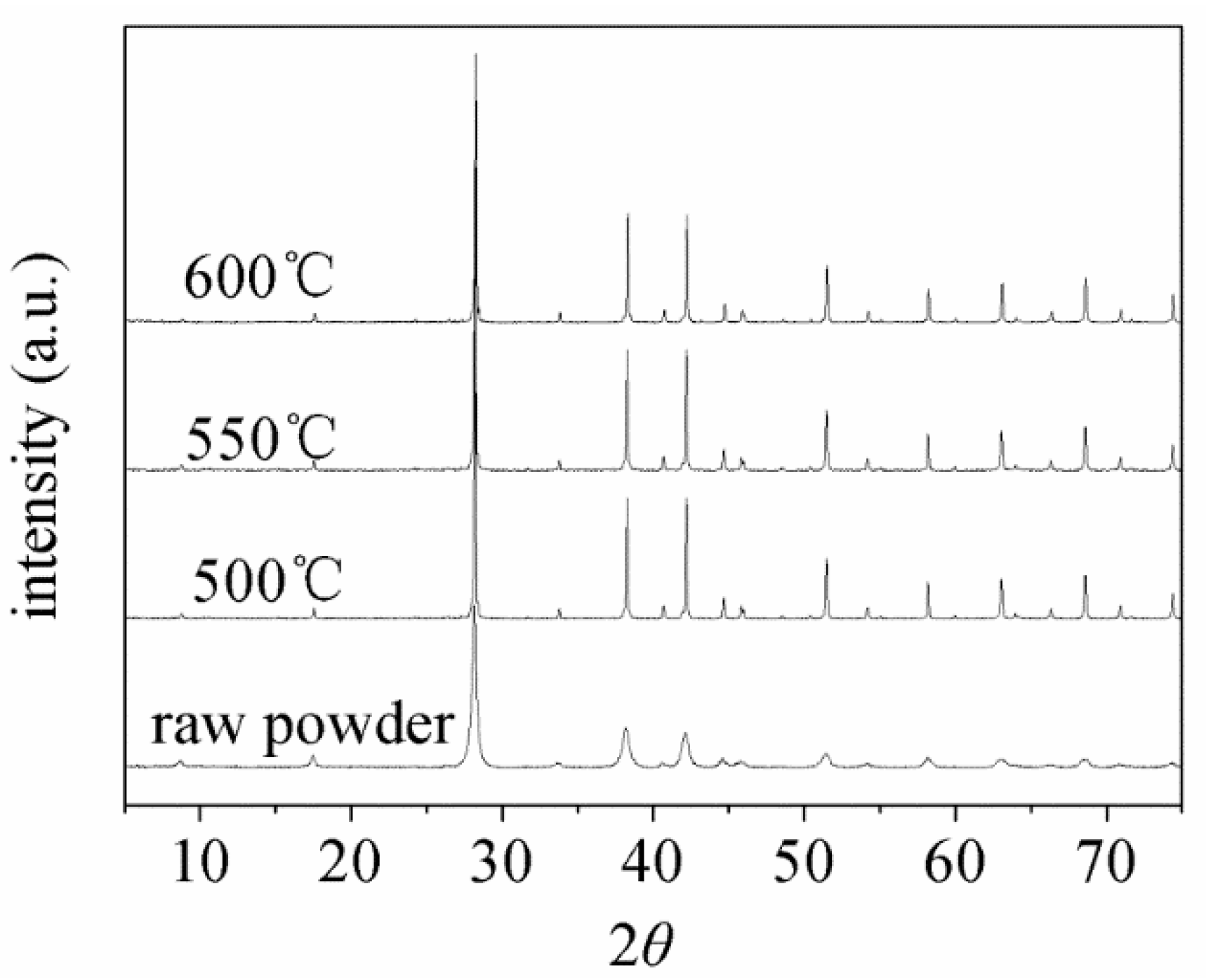
Figure 1 displays XRD patterns of BST raw powder and its thick films. The XRD pattern of the powder shows a single-phase structure and is well matched to the (Bi
0.48Sb
1.52)Te
3 crystallographic structure [
10,
11,
12]. The broadening diffraction peaks indicate that the particles are ultrafine. For films sintered at different temperatures, all the patterns do not demonstrate a visible difference, and are matched to the pure (Bi
0.48Sb
1.52)Te
3 material [
10,
11,
12]. The sharp XRD peaks of all films imply that grains of these specimens were coarsened and in the size of micro or submicron scale.
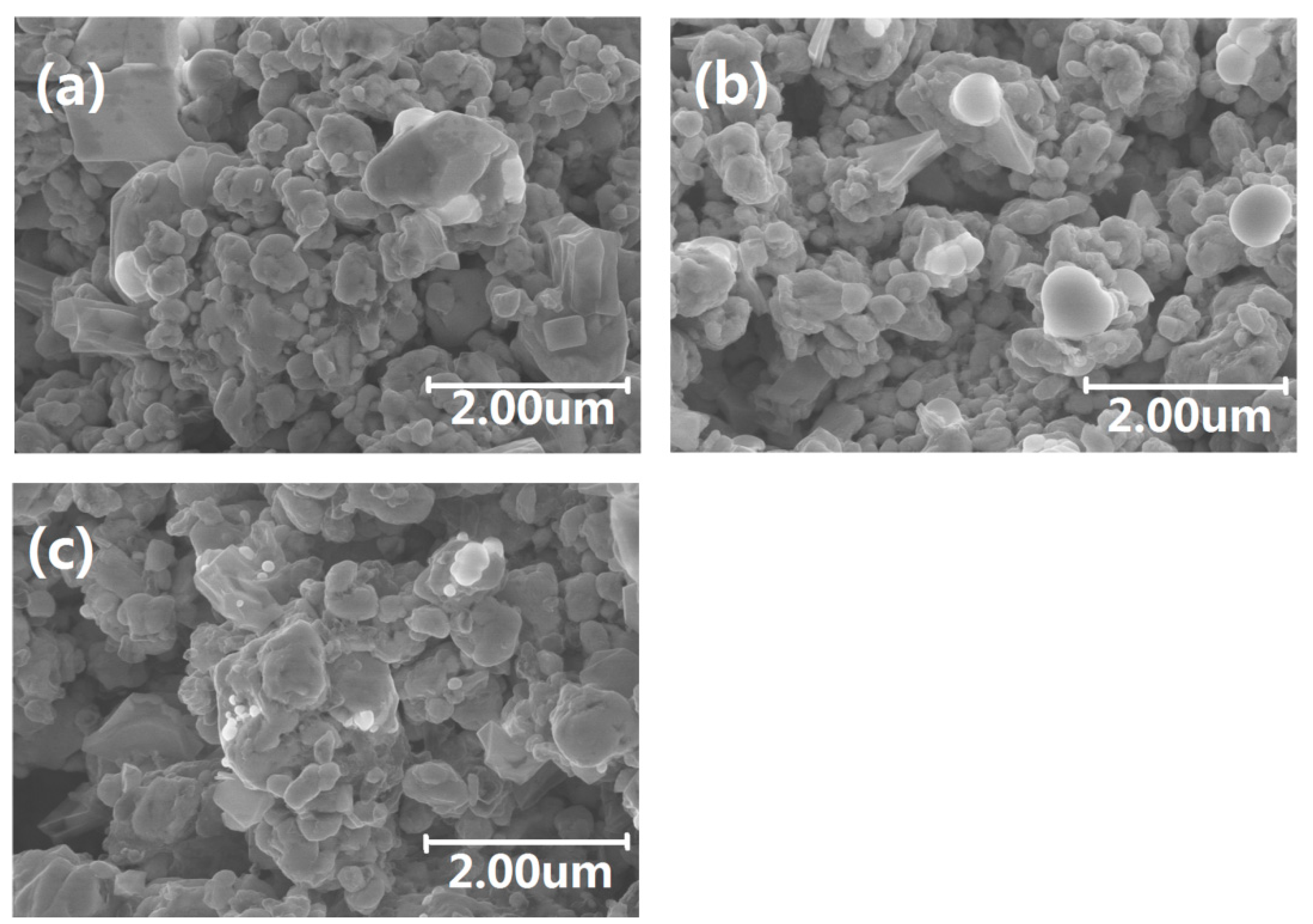
Figure 2a–c show SEM images of BST thick films annealed at 500 °C, 550 °C and 600 °C, respectively. It is clear that all samples are porous due to the evaporation of the organic substance from the slurry during the drying and annealing process. The grain size of all samples is in the range of 200–500 nm, which confirms the result of XRD diffraction in
Figure 1. It should be noted, that no obvious differences in grain size and porosity are observed among these thick films.
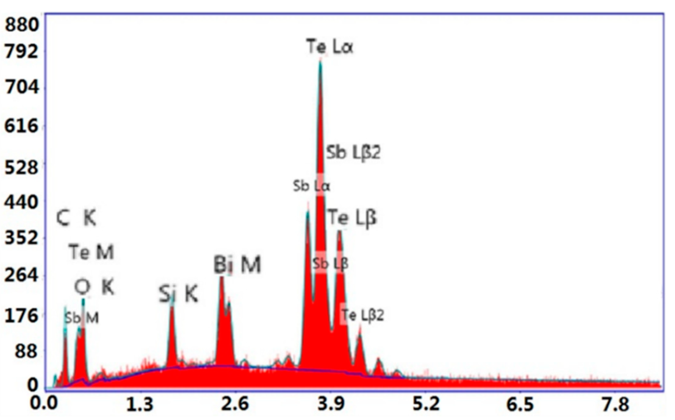
Figure 3 shows the EDX spectrum of the BST thick film annealed at 550 °C for 1 h in a 10
−2 Pa vacuum, and
Table 1 lists the element amount in this sample according to the spectrum. The at.% ratio of Si to O is about 1:2, revealing that the glass substrate contributed to the Si and O peaks in the spectrum. The amount of carbon element has an atomic percentage of around 34%, implying that organic solvent, dispersant and binder were not completely removed during the drying and sintering process. At high temperatures, some of these organic substances were pyrolyzed into carbon materials due to the deficiency of oxygen. By considering the fact that EDX can only give a rough quantity analysis, more detailed analysis of the microstructure using HRTEM and STEM-EDX will be carried out in the future to determine the polymorphy and distribution of carbon elements.
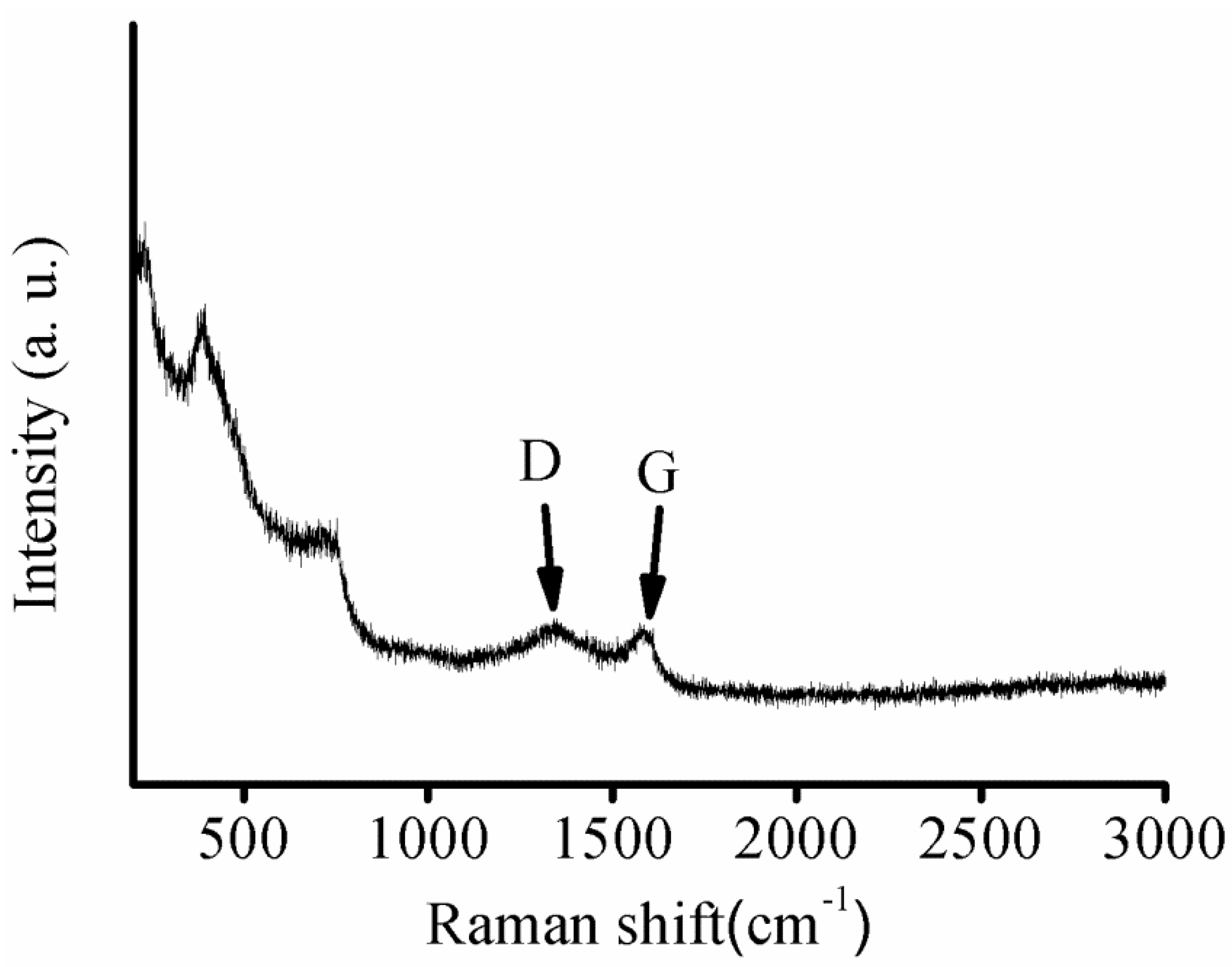
Figure 4 demonstrates a Raman spectrum of the BST thick film annealed at 550 °C for 1 h in 10
−2 Pa vacuum. Raman spectra of carbon materials are known to be sensitive to polymorphy. In general, the spectra can be analyzed according to the contribution of the “ordered carbon” (G peak) and the disordered carbon (D peak) [
13]. In
Figure 4, the G and D peaks have a similar intensity, as well as partially overlapping; therefore the carbon in BST films can be identified as active carbon.
In
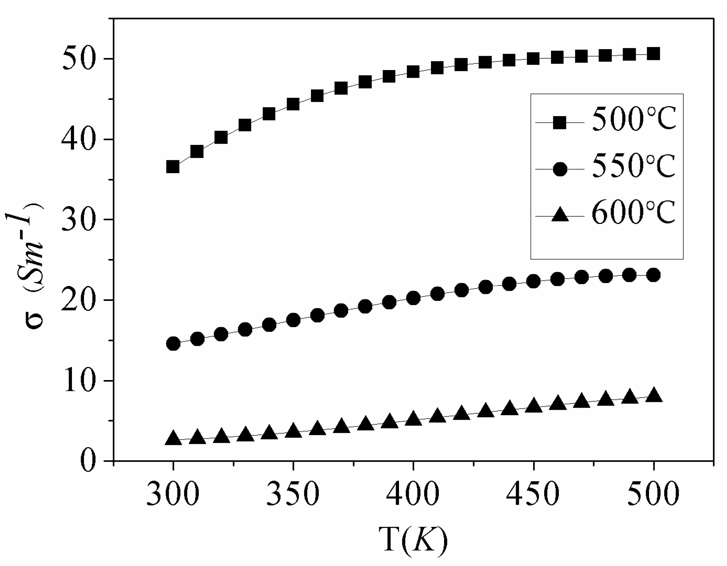
Figure 5 the electrical conductivity of BST thick films is plotted as a function of temperature. The absolute
σ values of all specimens are three orders of magnitude smaller than those of the bulk material, which is compatible with the reported results of a Bi
2Te
3 based alloy prepared with the screen printing method [
4,
5,
6]. At 25 °C, the electrical conductivity of these samples annealed at 500 °C, 550 °C and 600 °C are 36.4, 14.1 and 2.3 S/m, respectively. It is noted that the typical electrical conductivity of common bulk BST is 60 × 10
3 S/m [
10,
11,
12]. Low conductivity can be explained by two factors: (1) there are pores existing in the thick films which prevent better Ohm contact among particles; (2) some nonconductive carbon is distributed in the films to partially interrupt Ohm contact among particles. Conductivity of all samples shows an increase with the measurement temperature, which could be associated with an increase in the carrier concentration at high temperatures. It is shown clearly in
Figure 5 that as the annealing temperature increases, the conductivity of the thick film decreases. Such a phenomenon may be attributed to the deficiency of Te in BST thick films due to the evaporation of Te during the annealing process, as a similar phenomenon was also found in [
4,
5,
6]. The vapor pressure of Te is as low as 7.5 × 10
−5 mmHg at 500 °C, implying that Te evaporates easily at high temperatures.
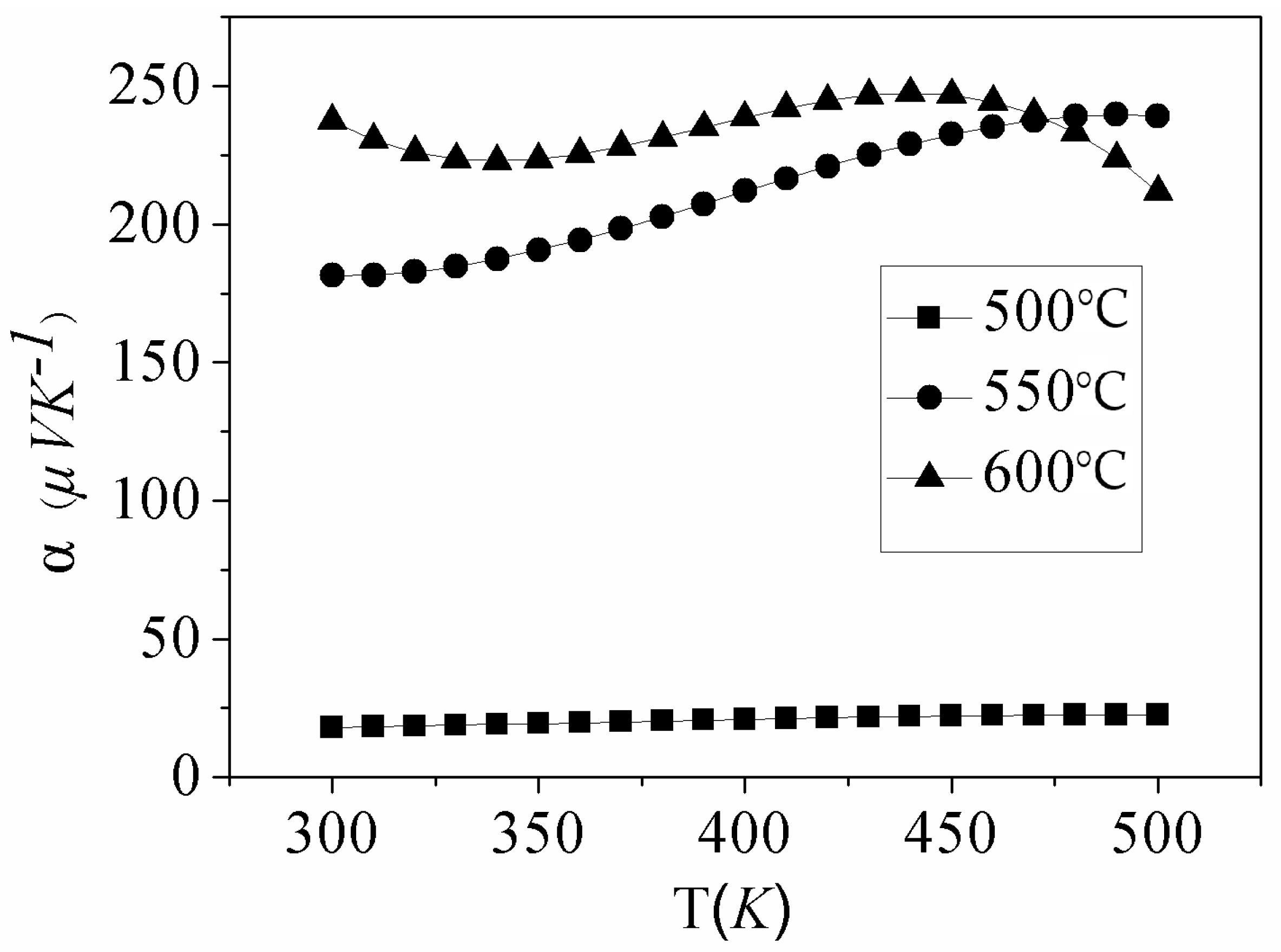
Figure 6 shows the Seebeck coefficient
α as a function of temperature for all BST thick films. The positive sign of the Seebeck coefficient indicates that BST thick films act as p-type materials. The results show that the Seebeck coefficient is quite sensitive to the annealing temperature of BST thick films. At 25 °C, the Seebeck coefficients of films annealed at 550 °C and 600 °C are 182 μV/K and 224 μV/K, respectively, which is comparable to 215 μV/K of bulk material [
10,
11,
12]. However, the film that annealed at 500 °C shows a very low Seebeck coefficient over the whole measured temperature range (18 μV/K at 25 °C). This low Seebeck coefficient might be related to more remnant carbon in the sample. Previous studies found that the temperature dependence of the Seebeck coefficient was susceptible to preparation processing, such as annealing conditions and doping concentrations, which is also confirmed in our work, for example, the sample annealed at 550 °C and 600 °C.
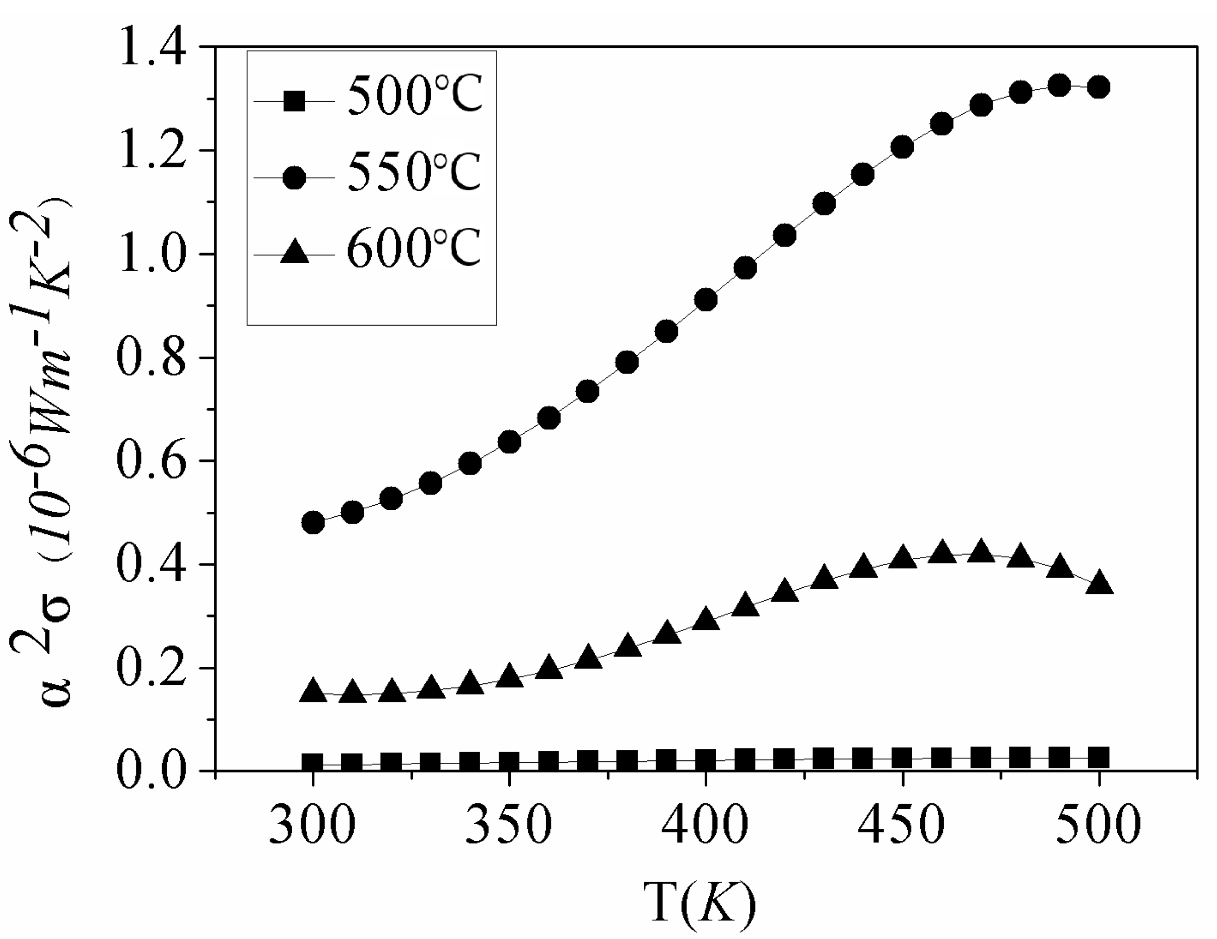
The thermoelectric power factor can be calculated from the formula
σα2, where
σ is the electrical conductivity and
α is the Seebeck coefficient. The power factor of the thick films as a function of temperature is presented in
Figure 7. At room temperature, the power factors of samples annealed at 500, 550 and 600 °C, are 0.01, 0.47 and 0.11 × 10
−6 W/mK
2, respectively. The sample that annealed at 550 °C possesses the highest power factor, which is compatible with the reported results of the Bi
2Te
3 based alloy prepared with the screen printing method [
4,
5,
6]. It should be noted that power factor of all films is three to four orders of magnitude smaller than 2.7 × 10
−3 W/mK
2 of BST bulk material [
10,
11,
12], which mainly comes from their low electrical conductivity. As shown in
Figure 5, electrical conductivity of BST thick films are three orders of magnitude smaller than that of BST bulk material.
