Article

Formulation and Analysis of Single Switch High Gain Hybrid DC to DC Converter for High Power Applications

by
Sathiya Ranganathan
1 and
Arun Noyal Doss Mohan
2,*
1
Department of Electronics and Communication Engineering, College of Engineering and Technology, SRM Institute of Science and Technology, Vadapalani Campus, Chennai 600026, India
2
Department of Electrical and Electronics Engineering, SRM Institute of Science and Technology, SRM Nagar, Kattankulathur, Chennai 603203, India
*
Author to whom correspondence should be addressed.
Electronics 2021, 10(19), 2445; https://doi.org/10.3390/electronics10192445
Submission received: 26 August 2021 / Revised: 24 September 2021 / Accepted: 28 September 2021 / Published: 8 October 2021

Abstract

:
The necessity for DC−DC converters has been rapidly increasing due to the emergence of RES-based electrification. However, the converter designed so far exhibits the drawbacks of lower efficiency and non-compactness in size. Hence, to rectify this problem, the new topology of a flyback converter for PV application is proposed in this work. The proposed converter exhibits reduced ripple in input current and enhances the conversion efficiency. Finally, the efficiency of this proposed converter is verified using MATLAB. The results indicate that this projected topology can be suitable for high voltage DC applications.

1. Introduction

Isolated DC−DC converters have been extensively utilized in many higher power applications, because of their higher efficiency, easy voltage gain and lower ripple content. As a result, numerous topologies of DC−DC converters have emerged in recent years. However, PV-based applications require high gain converters so as to increase their efficiency for high power applications.
The traditional DC−DC converters, namely BOOST and buck boost topology, exhibit high ripple content as their output [1,2,3,4]. Similarly, they also suffer from voltage polarity problems. Thus, to overcome this deficiency in the conventional converters, modifications in converter have been introduced. However, the gain of this converter is very small. Similarly, to overcome the leakage reactance issue, magnetically coupled converters have been developed. The main drawbacks of these converters are high ripple content and higher switching losses [5]. Hence, a new buck-boost topology was formulated by [6]. This circuit results in high power loss. Then, cascaded type converters [7] were introduced. However, in this circuit, as the capacitor is in operation under a discontinuous mode of operation, the efficiency is reduced.
This can be effectively solved by using the SEPIC converter [8]. It results in a lower duty cycle with increased gain. This in turn, decreases the voltage stress across the switches. Hence, ripples in the current are reduced. The SEPIC converter under bridgeless topology was developed by [9]. However, it is applicable only for high power AC applications. Thus, a modified SEPIC converter was formulated [10], which is suitable for medium power applications. For high power applications the Re-Lift converters have recently been developed [11,12]. They result in reduced voltage stress, but the main drawback is the high inductance.
LLC converters were introduced [13], for high power applications, but the utilization of transformers led to higher loss. Later, Ćuk converters came into existence [14,15,16]. Among these, the Luo converters are becoming more popular due to their high output gain and less voltage ripple at the output [17,18,19,20].While designing the converters, the switches play a major role. This has led to the development of multichip power modules (PMs) using SiC MOSFETs [21]. These types of devices require a cautious design to handle (i) the power dissipated by devices, and (ii) their high switching frequency [22]. Similarly, the designers should concentrate on electrothermal (ET) effects and the impact of parasitics [23]. So, many researchers have concentrated on the design of PMs using SiC MOSFETs. This approach is utilized while designing a DC converter for renewable energy applications. Keeping this in view, this work proposed a hybrid combination of the Luo with flyback converter which exhibits a higher voltage gain and less ripple content with SiC MOSFETs as switches.

2. Design of Proposed System

In this configuration, the formulated converter (specifications given in Appendix A) acts as a voltage regulator between PV source and load. Figure 1 presents the block diagram of a formulated work.
Design procedure of the proposed system is as follows.

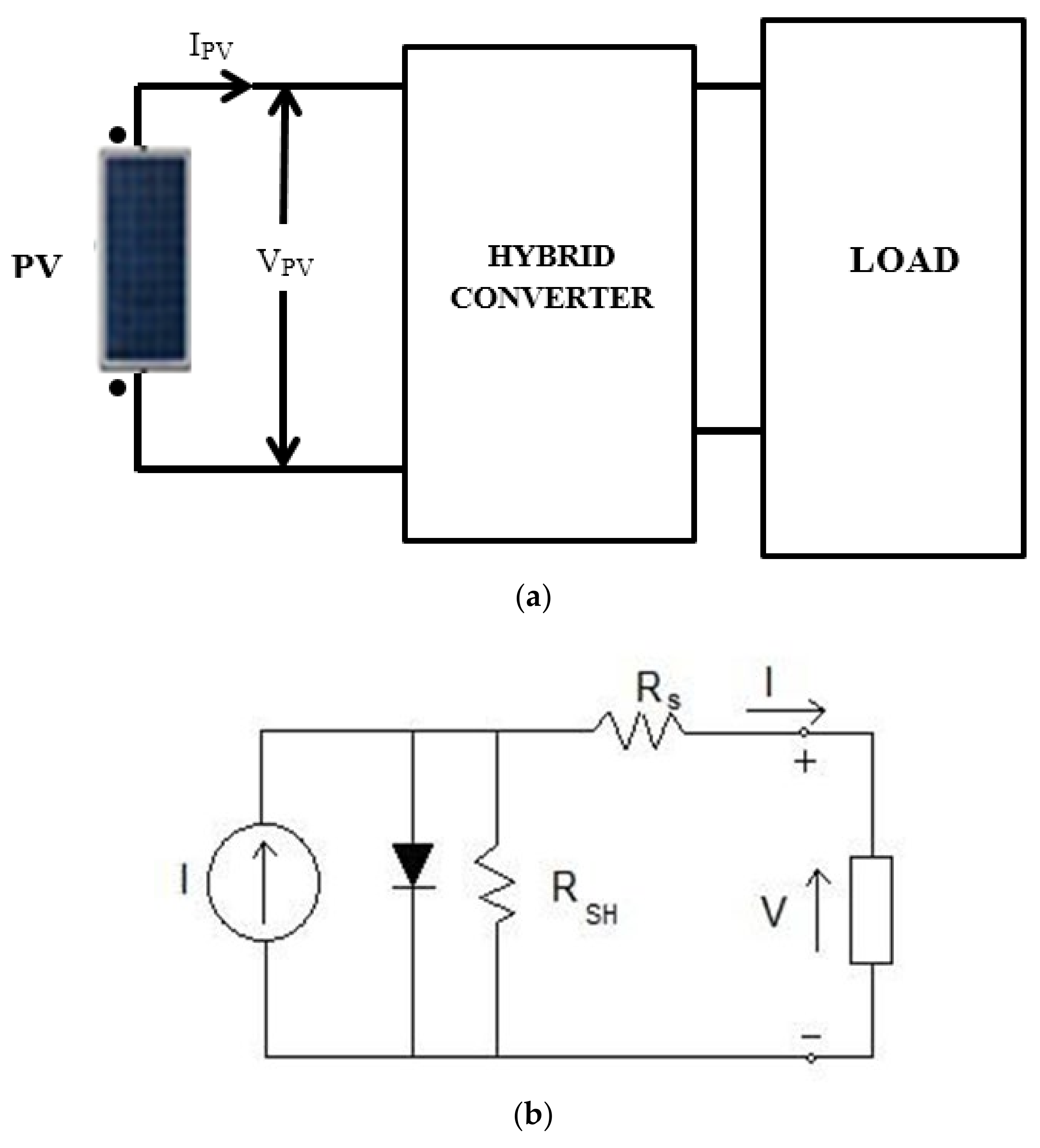
2.1. Design of PV Array

A PV array of capacity 5 kW is chosen for the proposed design. The design of chosen PV array is depicted as follows.
A mathematical description of a photovoltaic cell and its equivalent circuit is depicted in Figure 1b.
The equivalent circuit of this model comprises a current source, series and parallel resistor and a diode. Thus the output current obtained from the photovoltaic array is given as
I = Isc − Id
where
Isc—Short circuit current
Id—Current across the diode
Thus, the proposed PV array can be designed [24,25,26,27,28] as follows
For a 5 kW, 250 V, current at MPP (Impp) can be valued as
Impp = Pmpp/Vmpp.
From this, the number of modules connected in parallel/series is calculated as follows
No. of series modules,
Ns = Vmpp/Vm
No. of parallel modules,
Np = Impp/Im

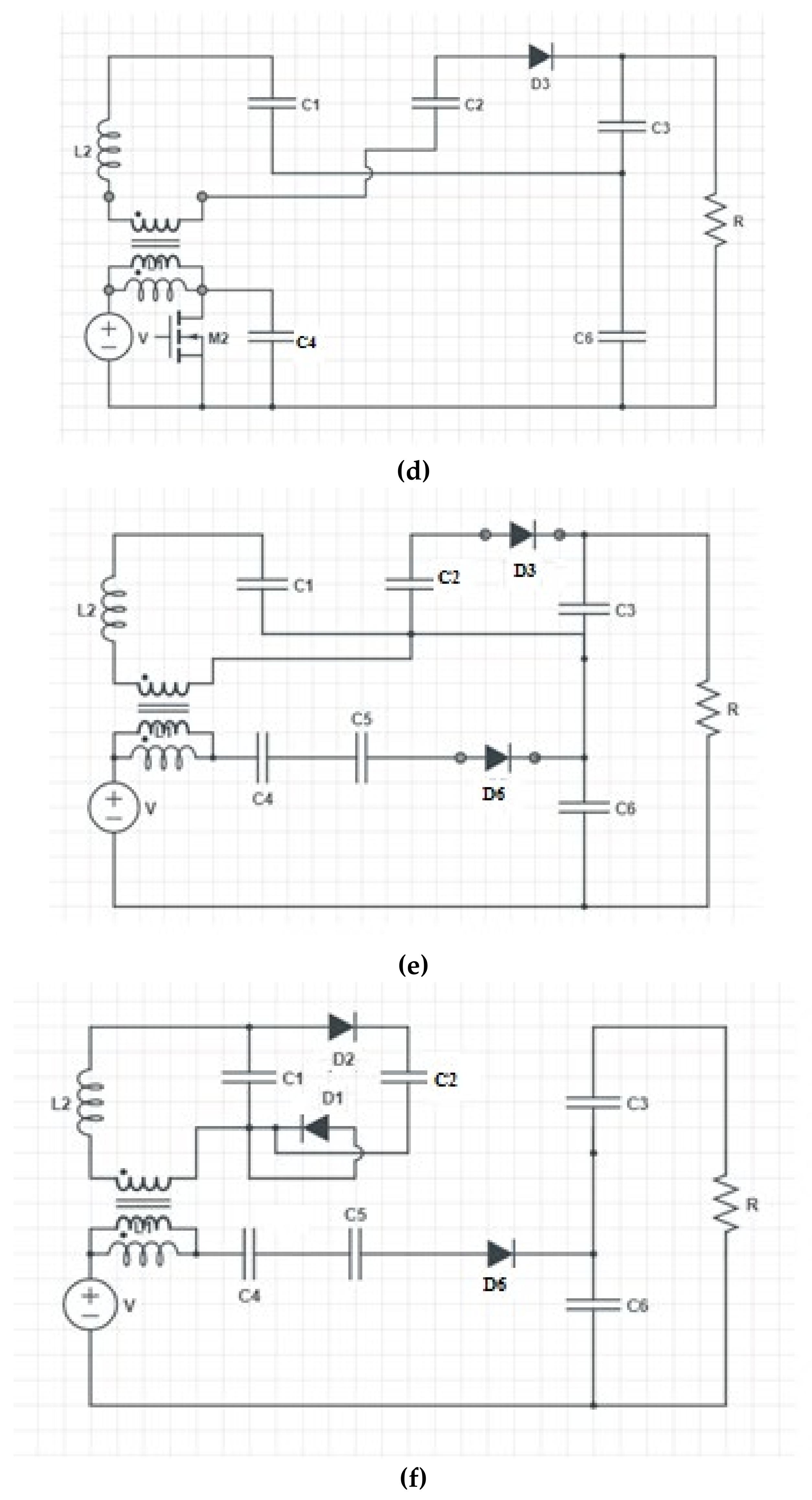
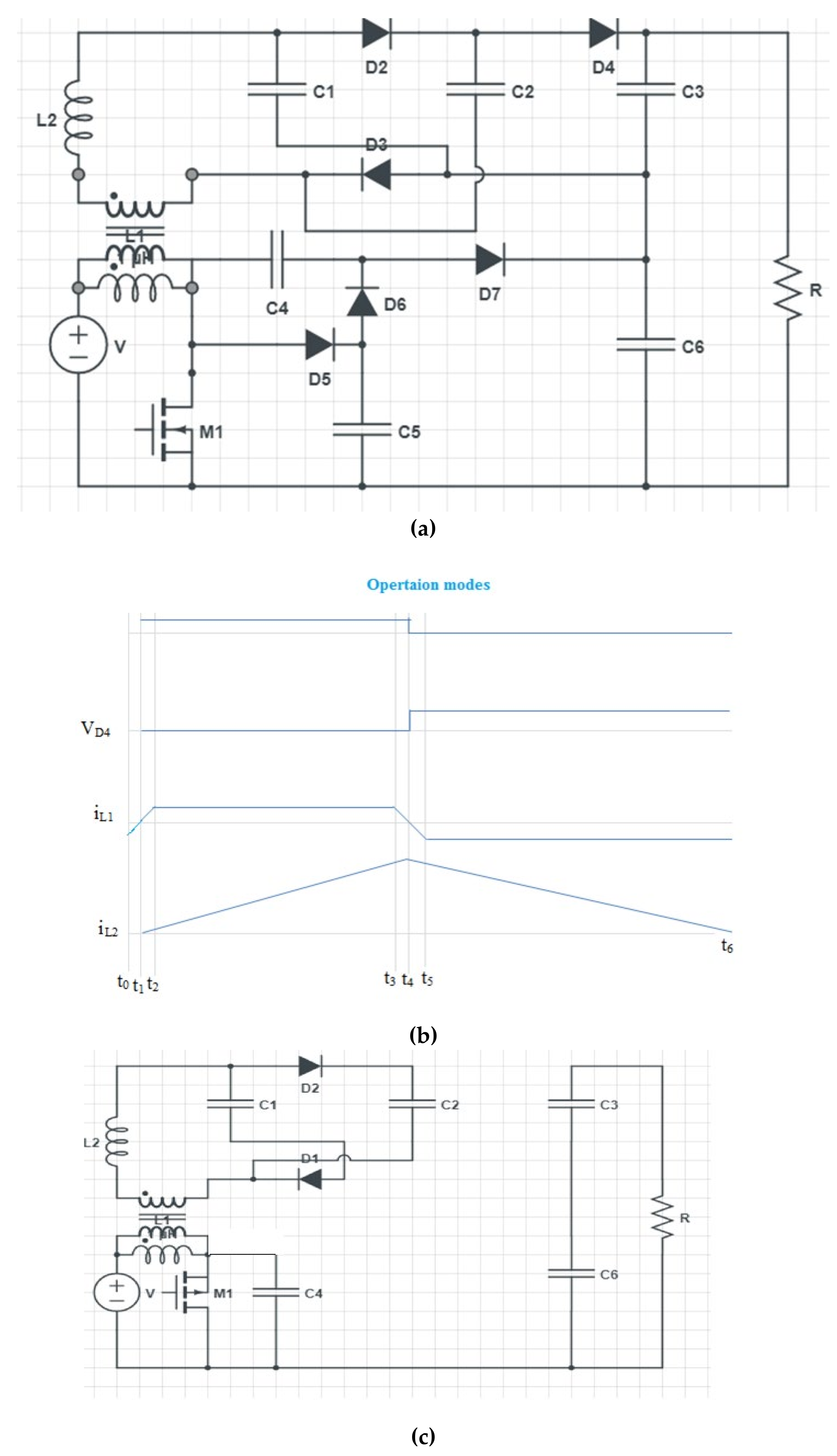
2.2. Proposed Converter

This proposed converter is a combination of a switched inductor, Luo and flyback converter. The proposed converter is shown in Figure 2a and its waveforms are shown in Figure 2b.
The advantage of the proposed converter is as follows: it provides continuous operation with the help of a coupled inductor.
Thus, an operation of a circuit is considered as six modes and is described below
Mode 1 (t0 − t1)
All the charges in the capacitors are nullified at this condition (t = t0).
Mode 2 (t1 − t2)
Switch S1 is turned on at zero voltage during t = t1.Thus, the current across ilm is given as
di lm dt = V 1 + V c n L m
where n-turns is the ratio of the coupled inductor.
In this circuit, during S1 ON the current induced on the secondary side of the coupled inductor starts charging the switching capacitor (C1 and C2).
Therefore, the current on the secondary side of the coupled inductor, il2, charges C3 and C4.
di lm dt = V 1 + 2 V c n L m
At that time, il2 is negative and hence its magnitude starts decaying.
Mode 3 (t2 − t3)
At this time, il2 reaches zero. Hence, the change of the direction in il2, makes the C1 and C2 discharge their charges to C3. Thus, current across the inductor im during this interval is depicted as
di lm dt = V 1 + 2 V c V c 3 n L m
Mode 4 (t3 − t4)
During t = t3, S1 is turned off. The current across im charges Vc4.
However, Vc4 is smaller than Vo, the voltage stress over S1 is comparatively low. Hence, the additional clamp circuit is not required.
Mode 5 (t4 − t5)
In this stage, again il2 gets reversed and current across the inductor im is about
di lm dt = V 1 V C 4 + V b n L m
Mode 6 (t5 − t6)
During t = t5, the current across the inductor remains the same as the previous mode.
Thus, the output voltage (Vo) of this converter can be calculated as
V o = V C 3 + V C 6
Some modes of operation (mode 1 and mode 5) are ignored.
Then by relating voltage second balance analysis over (Lm and L2) in modes 3 and 6, the relationship between V1, VO, VC, VC3 and VC4 can be derived as,
V C 4 = 2 D 1 D V 1
V c = D 1 + D V C 3
Then by rearranging Equations (5)–(8) the voltage gain of this proposed converter can be expressed as,
M = V o V 1 = 2 + n + nD D 1 D
From the above equation, it is concluded that based on the turns ratio (n) between mutual inductance (Lm1 and Lm2), the voltage gain of the converter can be varied.
Analysis of Ripple Minimization
While considering ripple minimization, the capacitor and inductors utilized in design should be considered as larger as given in equation 3. But during the switching period, the voltage across the inductor is zero. Similarly, voltage ripple across C1 and C4 are also zero due to large value. Hence, the input voltage retains constant value over the switching period. The ripple current across the inductor is considered as zero as average inductor voltage is zero.
Analysis of switching loss
When the switch is turned on, negative current through the diode discharges and creates zero voltage condition. Thus, in turn reduces the turn-on loss then hard switching. So, it is concluded that switching loss is reduced.

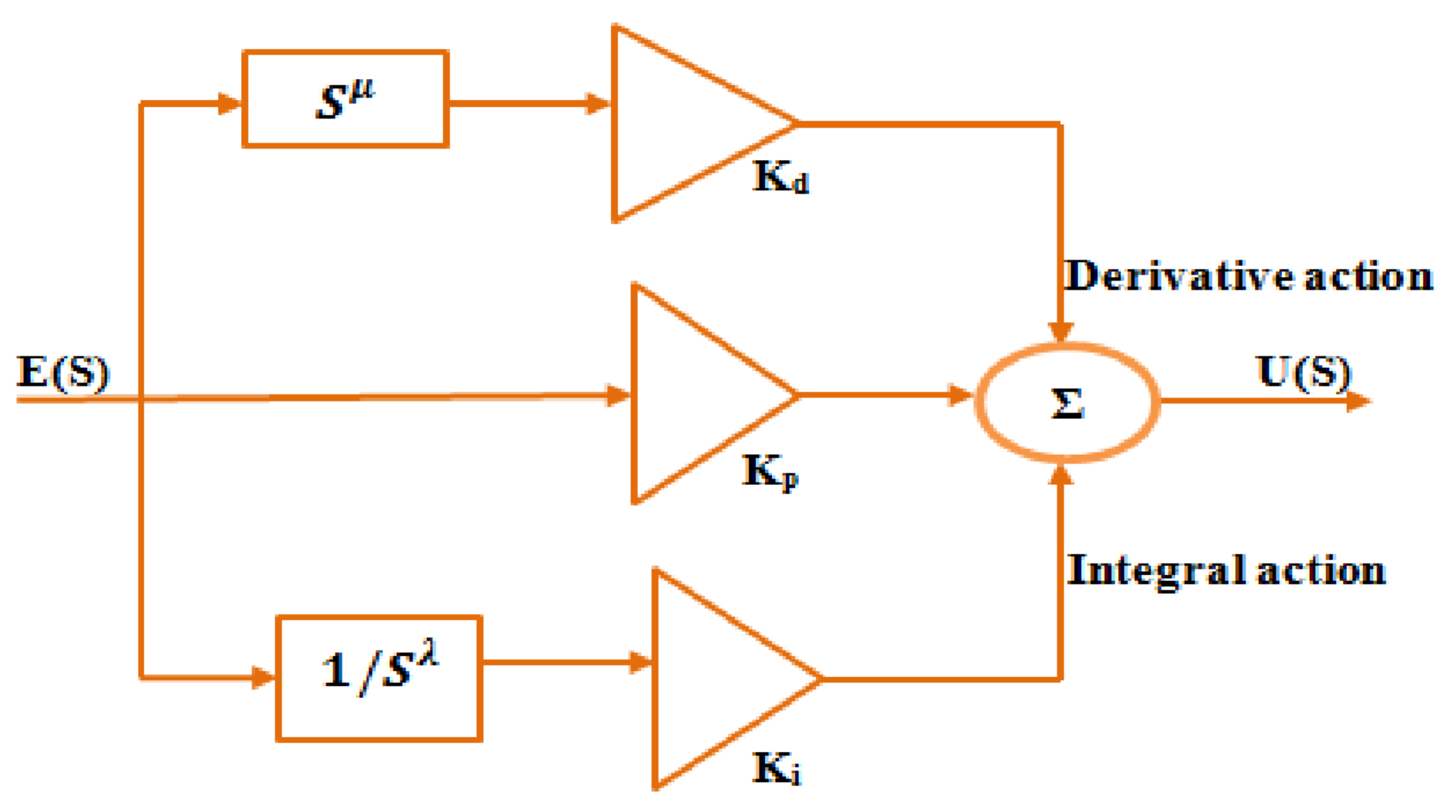
2.3. Design of Controllers

FOPID Controller

In order to improve the system control performances, in many industrial applications fractional order PID controllers have recently been used. The FOPID controller is the extension of the conventional PID controller based on fractional calculus and is shown in Figure 3.
The transfer function of PI λ D µ is given in the equation as,
C S = U S E S = K p + K i S λ + K d   S μ
The positive real numbers are λ and µ, respectively.
The proportional, integral and derivative gain constants are Kp, Ki and Kd, respectively.

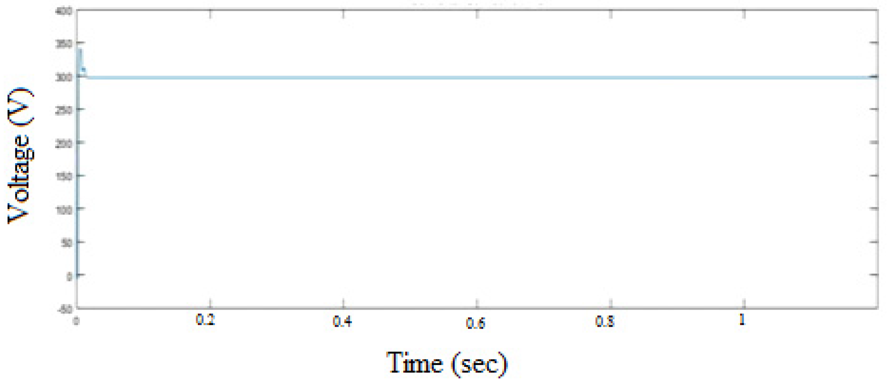
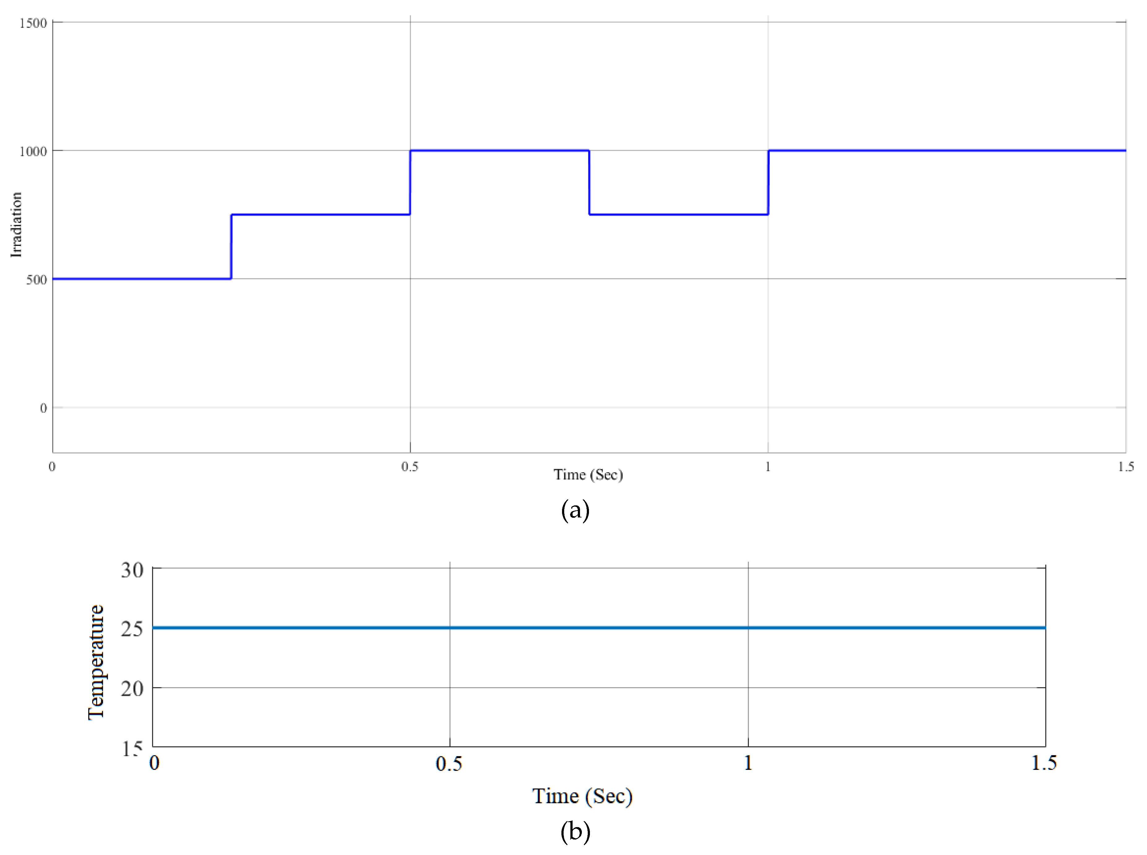
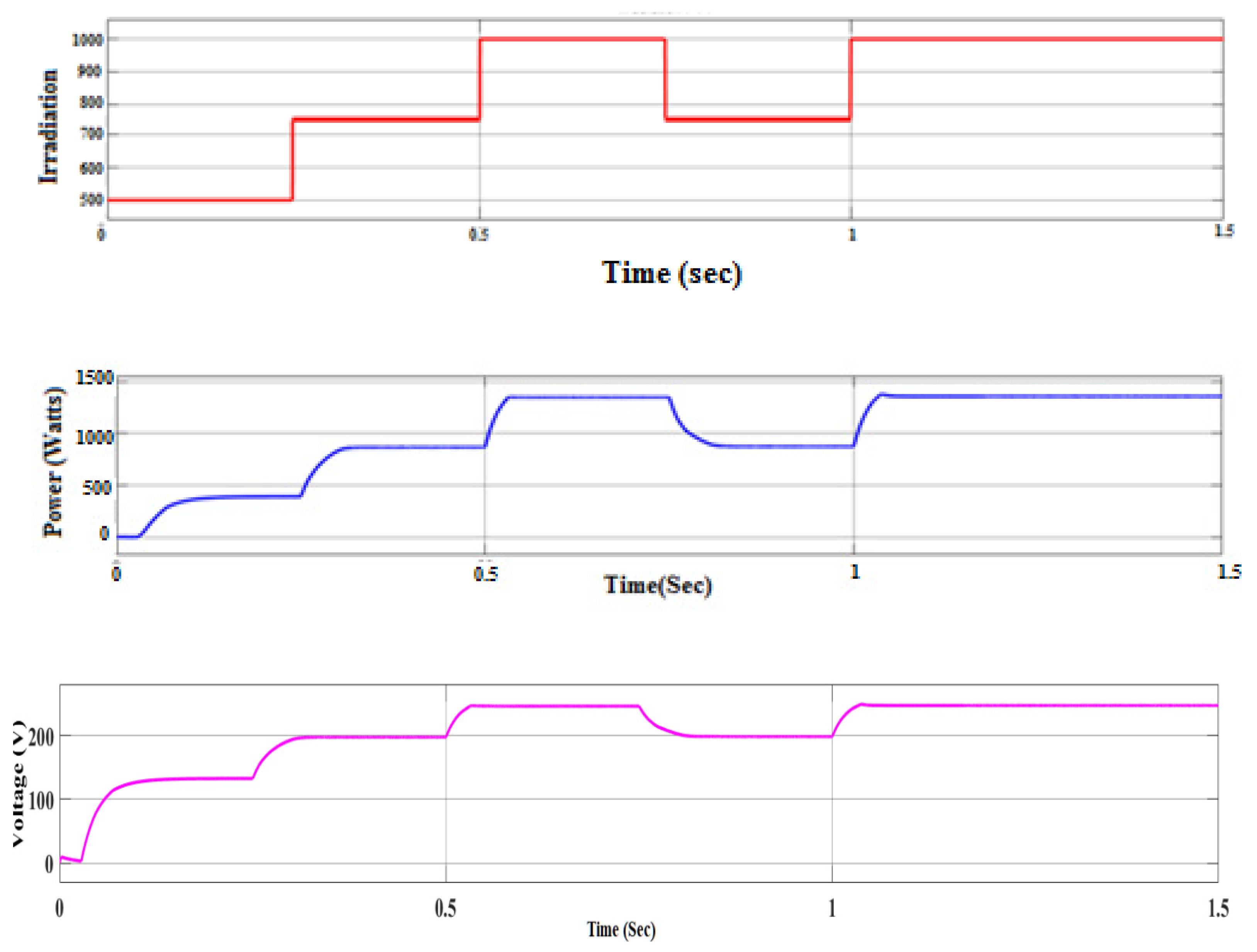
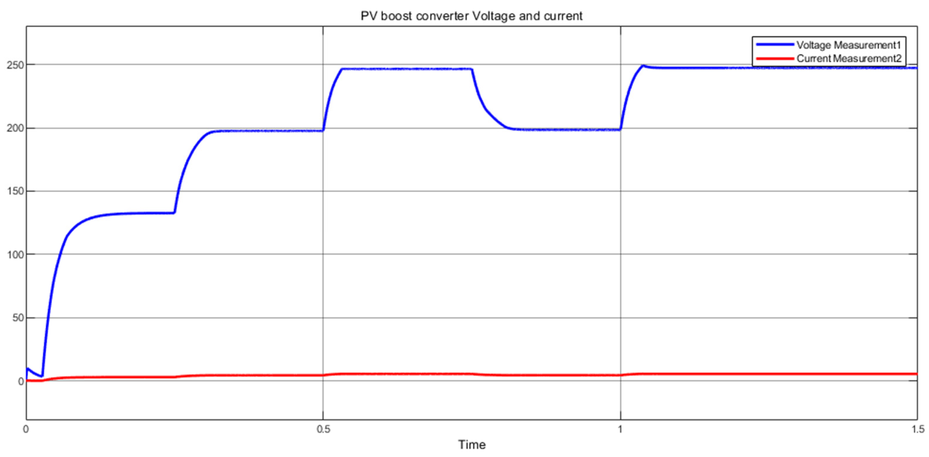
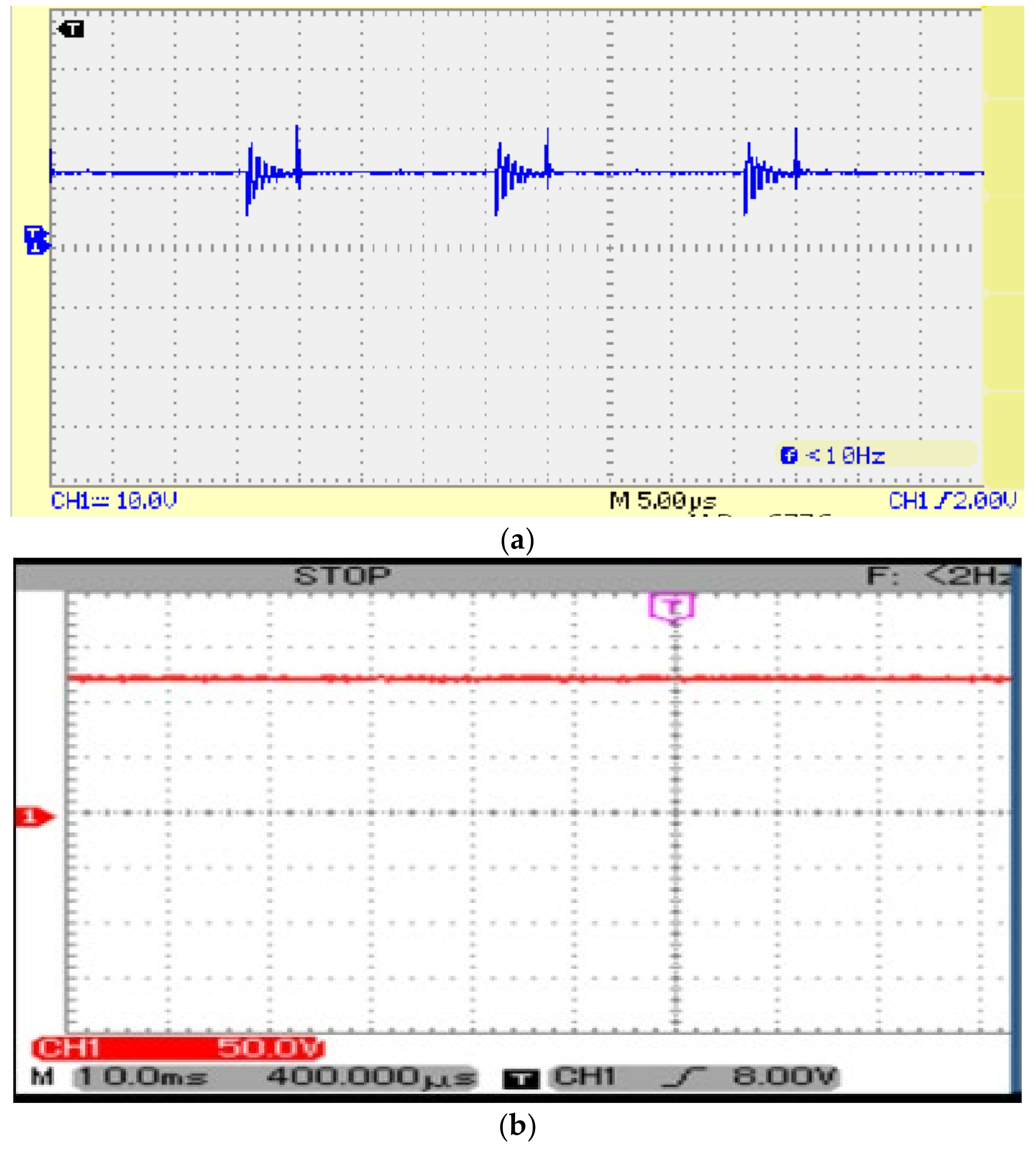
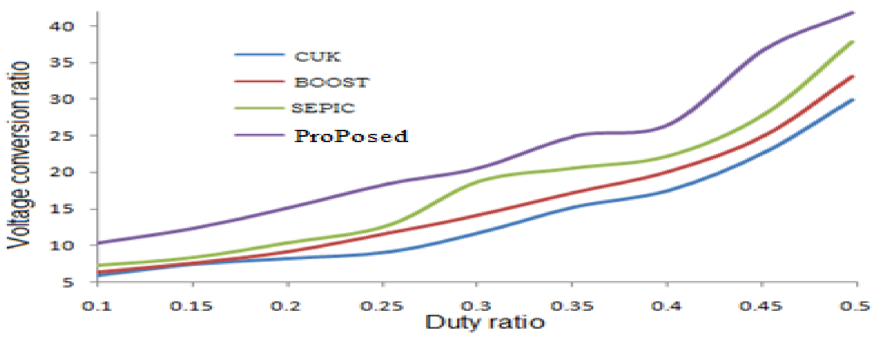
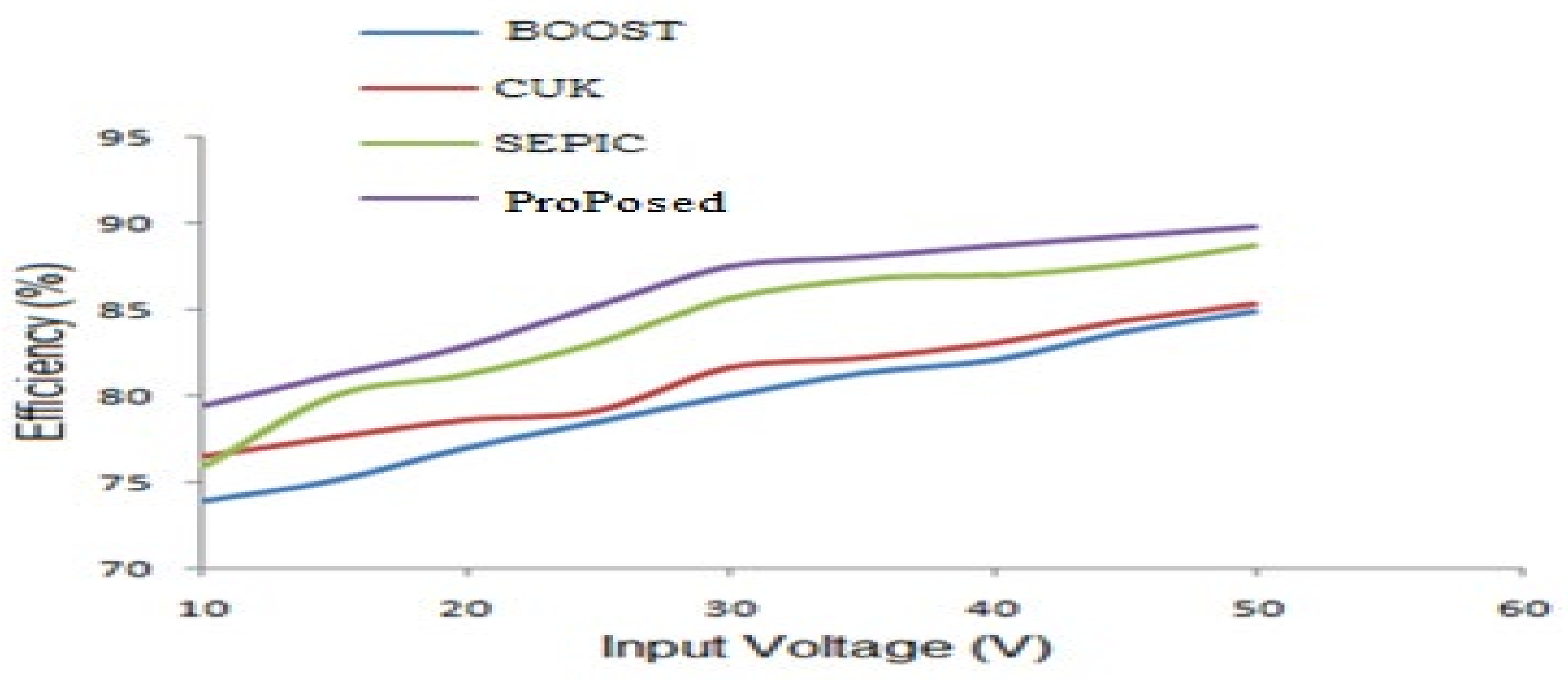
3. Simulation Results and Discussion

To demonstrate the effectiveness of the proposed converter, simulations were
performed appropriately using MATLAB software.
Performance of the proposed system with PV under open loop control
The input parameters of a solar array are irradiation and temperature. In this work, the irradiation value is varied accordingly, as shown in Figure 4. Similarly, the temperature remains constant at 25 °C.
Figure 5 shows the PV indices such as solar insolation level; PV output power and proposed converter voltage. From the above Figure, it is also concluded that the energy obtained from PV is maximized with the help of the proposed converter and a stable power with less oscillations is obtained.
Performance of Proposed Converter
Figure 6 depicts the output current and voltage of the proposed converter.
From the above figure, it is observed that the high frequency switching eliminates the ripple contents in the output.
Closed loop analysis
From the above analysis, it is depicted that the open circuit voltage is highly influenced by the increase in the panel temperature. The drop in the open circuit voltage with the increase in temperature, PV output power will decrease. Hence the voltage supplied to the load gets distorted. Hence in order to maintain the constant voltage at the load side, Controllers are implemented.
Figure 7 displays the output voltage of the proposed converter.
Hardware analysis
Thus, to examine the effectiveness of the proposed converter simulated in MATLAB, a 100 W prototype converter was modeled. Figure 8 and Figure 9 depict the pictures of the prototype of the proposed converter examined in the laboratory.
Figure 10a,b depicts the input/output voltage and current waveforms of the proposed converter.
Figure 10c depicts the switching pulses applied to the switch S1 of the proposed converter, which is about 0.50.
Figure 11 compares the voltage gain (M) of the Different DC−DC converter under various duty ratios (k).
From the above graph, Figure 11, shows that voltage transfer gain (M) of boost, Ćuk and SEPIC DC–DC converters is identical. However, the proposed converter has a higher voltage transfer gain. When choosing a DC−DC converter, efficiency plays a vital role for RES applications. Figure 12 shows the comparison of the efficiency of various converters with respect to input voltage.
From the above graph, it is inferred that the proposed converter has a higher efficiency at higher input voltage. Hence, it is clear that for medium-power applications the Ćuk, and SEPIC converters are more suitable whereas boost converters are suitable for applications which need only low power. Thus, it is visualized that for high power RES, the proposed converter is the suitable one.
From the Table 1, it is concluded that the utilization coupled inductor in this converter improves the voltage gain of the converter by more than 10 times that of a conventional boost converter. Hence, this converter can be utilized for PV applications. Thus, the voltage stress across the switch of the proposed converter is very low compared to that of the conventional boost converter. Hence, the proposed converter exhibits lower conduction loss.
Table 2 deals with the comparisons with the other converters which implement coupled-inductor topology. From the results, it was found that the proposed converter exhibited higher voltage gain than the others.

4. Conclusions

In this study, a hybrid DC−DC converter was designed for high power applications. This is the combination of a Luo converter with a flyback converter. In this work, a voltage multiplier circuit was implemented to boost the voltage level. Thus, the operation of the circuit was carried out with a single switch; the switching losses were comparatively low.Thus the performance of the formulated converter was examined using both simulation and experimental results. To increase the dynamic behavior of the converter, controllers were implemented. In this work, a FOPID controller was chosen to improve the dynamic behavior of the proposed system. From the simulation results, the efficiency of the proposed FOPID controller is proven. From the simulated and experimental results, it is evident that this converter exhibits higher efficiency.

Author Contributions

Conceptualization, S.R. and A.N.D.M.; methodology, S.R.; software, S.R.; validation, S.R., A.N.D.M.; formal analysis, S.R.; investigation, S.R.; resources, S.R.; data curation, S.R.; writing—original draft preparation, S.R.; writing—review and editing, S.R.; visualization, S.R.; supervision, A.N.D.M.; project administration, S.R.; funding acquisition, A.N.D.M.All authors have read and agreed to the published version of the manuscript.

Funding

This research received no external funding.

Conflicts of Interest

The authors declare no conflict of interest.

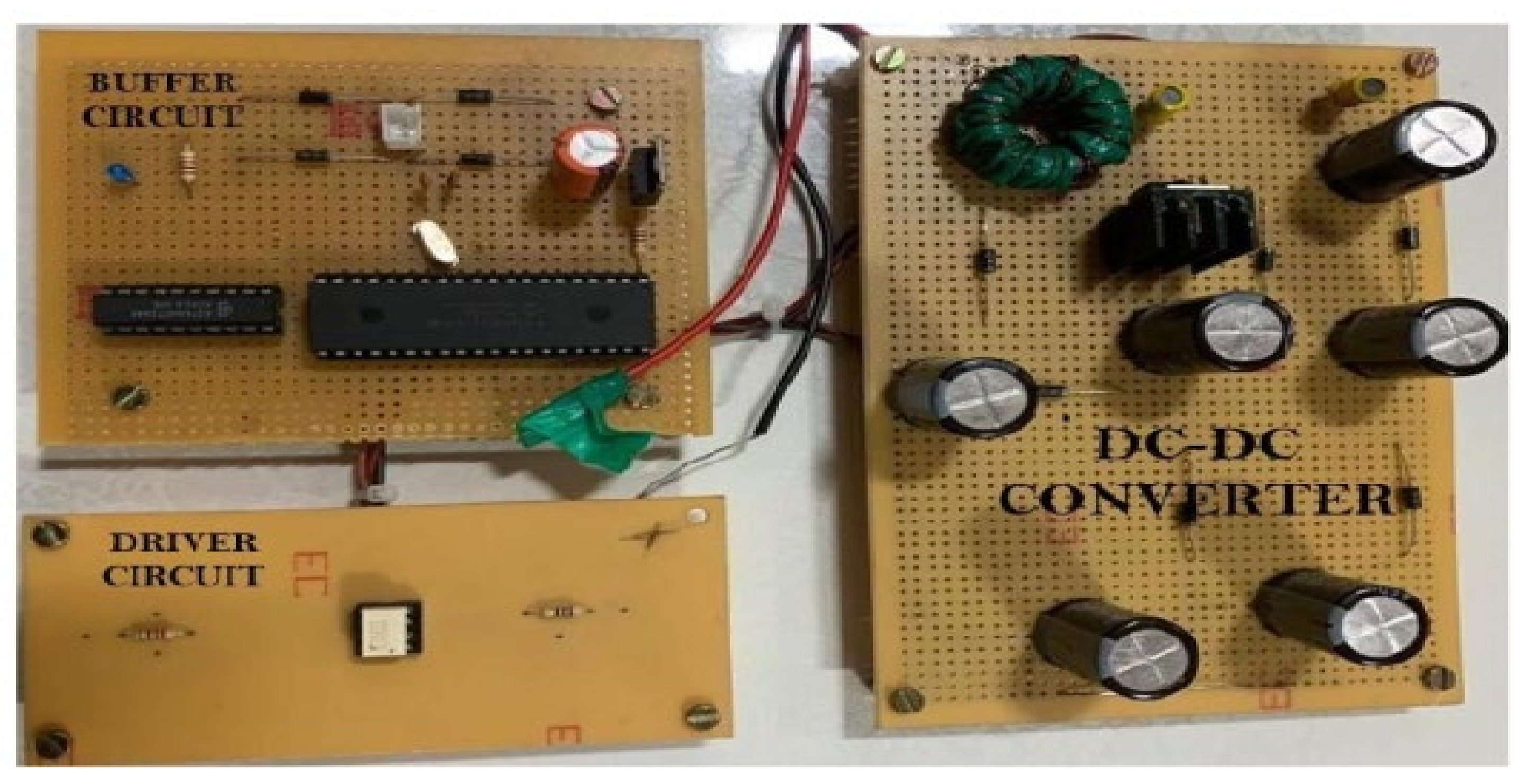
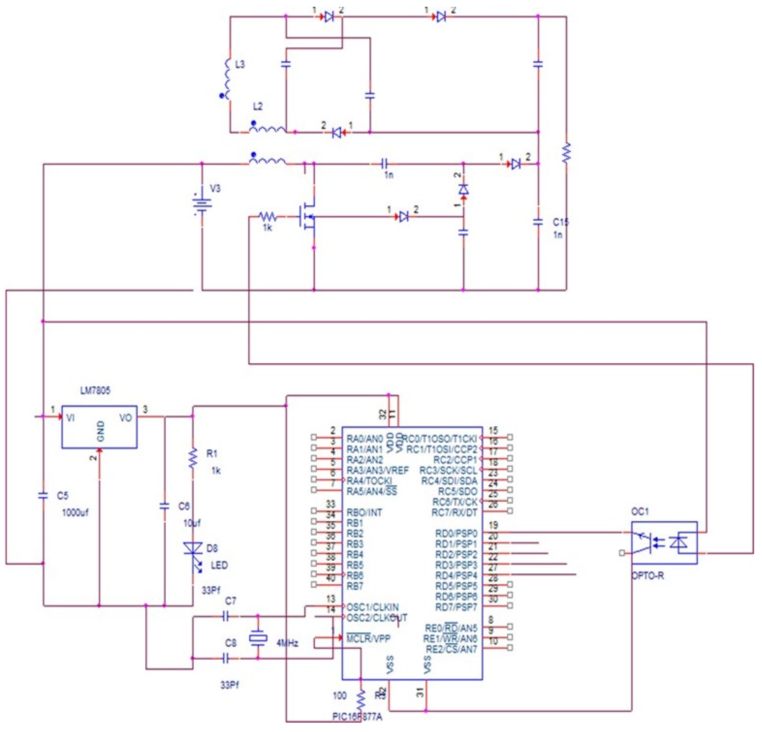
Appendix A. Proposed Converter

ParametersValues
fsw20 kHz
C500 mF
C1, C236 mF
C3, C457 μF
Lm617 mH
Lk217.1 μH

References

  1. Park, K.B.; Moon, G.W. Non isolated high step-up stacked converter based on boost-integrated isolated converter. IEEE Trans. Power Electron. 2011, 26, 577–587. [Google Scholar] [CrossRef]
  2. Liu, H.; Ji, Y.; Wang, L.; Wheele, P. A family of improved magnetically coupled impedance network Boost DC-DC converters. IEEE Trans. Power Electron 2018, 33, 3697–3702. [Google Scholar] [CrossRef]
  3. Hwu, K.I.; Peng, T.J. A novel buck-boost converter combining KY and buck converters. IEEE Trans. Power Electron. 2012, 27, 2236–2241. [Google Scholar] [CrossRef]
  4. Lu, Y.; Wu, H.; Sun, K.; Xing, Y. A family of isolated buck-boost converters based on semi active rectifiers for high-output voltage applications. IEEE Trans. Power Electron. 2016, 31, 6327–6340. [Google Scholar] [CrossRef]
  5. Pang, S.; Nahid-Mobarakeh, B.; Pierfederici, S.; Phattanasak, M.; Huangfu, Y.; Luo, G.; Gao, F. Interconnection and damping assignment passivity-based control applied to on-board DC-DC power converter system supplying constant power load. IEEE Trans. Ind. Appl. 2019, 55, 6476–6485. [Google Scholar] [CrossRef]
  6. Moon, B.; Jung, H.Y.; Kim, S.H.; Lee, S.H. A modified topology of two-switch buck-boost converter. IEEE Trans. Power Electron. 2017, 5, 17772–17780. [Google Scholar] [CrossRef]
  7. Badawy, M.O.; Sozer, Y.; Abreu-Garcia, J.A.D. A novel control for a cascaded buck-boost PFC converter operating in discontinu- ous capacitor voltage mode. IEEE Trans. Ind. Electron. 2016, 63, 4198–4210. [Google Scholar] [CrossRef]
  8. Park, K.B.; Moon, G.W.; Myung-Joon, Y. Non isolated high step-up boost converter integrated with Sepic converter. IEEE Trans. Power Electron. 2010, 25, 2266–2275. [Google Scholar] [CrossRef]
  9. Yang, J.W.; Do, H.L. Bridgeless SEPIC converter with a ripple-free input current. IEEE Trans. Power Electron. 2013, 28, 3388–3394. [Google Scholar] [CrossRef]
  10. Bianchin, C.G.; Gules, R.; Badin, A.A.; Romaneli, E.F.R. High-power-factor rectifier using the modified SEPIC converter operating in discontinuous conduction mode. IEEE Trans. Power Electron. 2015, 30, 4349–4364. [Google Scholar] [CrossRef]
  11. Luo, F.L.; Ye, H. Super-lift boost converters. IET Power Electron. 2014, 7, 1655–1664. [Google Scholar] [CrossRef]
  12. Berkovich, Y.; Axelrod, B.; Madar, R.; Twina, A. Improved Luo converter modifications with increasing voltage ratio. IET Power Electron. 2015, 8, 202–212. [Google Scholar] [CrossRef]
  13. Shih, L.C.; Liu, Y.H.; Luo, Y.F. Adaptive DC-link voltage control of LLC resonant converter. Trans. Power Electron. Appl. 2018, 3, 187–196. [Google Scholar] [CrossRef]
  14. Jiang, W.; Chincholkar, S.H.; Chan, C.Y. Improved output feedback controller design for the super-lift Re-lift Luo converter. IET Power Electron. 2017, 10, 1147–1155. [Google Scholar] [CrossRef]
  15. Yang, H.T.; Chiang, H.W.; Chen, C.Y. Implementation of bridgeless Cuk power factor corrector with positive output voltage. IEEE Trans. Ind. Appl. 2015, 51, 3325–3333. [Google Scholar] [CrossRef]
  16. Joseph, K.D.; Daniel, A.E.; Krishnan, A.U. Interleaved Cuk converter with improved transient performance and reduced current ripple. J. Eng. 2017, 7, 362–369. [Google Scholar]
  17. Ferrera, M.B.; Litran, S.P.; Duran, E.; Andujar, J.M. A converter for bipolar DC link based on SEPIC Cuk converter. IEEE Trans. Power Electron. 2015, 30, 6483–6487. [Google Scholar] [CrossRef]
  18. Gnanavadivel, J.; Yogalakshmi, P.; Kumar, N.S.; Veni, K.K. Design and development of single phase AC-DC discontinuous conduction mode modified bridgeless positive output Luo converter for power quality improvement. IET Power Electron. 2019, 12, 2722–2730. [Google Scholar] [CrossRef]
  19. Muhammad, K.S.B.; Lu, D.D.C. ZCS bridgeless boost PFC rectifier using only two active switches. IEEE Trans. Ind. Electron. 2015, 62, 2795–2806. [Google Scholar] [CrossRef]
  20. Singh, B.; Bist, V.; Chandra, A.C.; Al-Haddad, K. Power factor correction in bridgeless Luo converter-fed BLDC motor drive. IEEE Trans. Ind. Appl. 2015, 51, 1179–1188. [Google Scholar] [CrossRef]
  21. Scognamillo, C.; Catalano, A.P.; Borghese, A.; Riccio, M.; d’Alessandro, V.; Breglio, G.; Irace, A.; Tripathi, R.N.; Castellazzi, A.; Codecasa, L. Electrothermal modeling, simulation, and electromagnetic characterization of a 3.3 kV SiC MOSFET power module. In Proceedings of the 2021 33rd International Symposium on Power Semiconductor Devices and ICs (ISPSD), Nagoya, Japan, 30 May–3 June 2021; pp. 123–126. [Google Scholar]
  22. Hussein, A.; Mouawad, B.; Castellazzi, A. Dynamic performance analysis of a 3.3 kV SiC MOSFET half-bridge module with parallel chips and body-diode freewheeling. In Proceedings of the 2018 IEEE 30th International Symposium on Power Semiconductor Devices and ICs (ISPSD), Chicago, IL, USA, 13–17 May 2018; pp. 13–17. [Google Scholar]
  23. Catalano, A.P.; Scognamillo, C.; d’Alessandro, V.; Castellazzi, A. Numerical simulation and analytical modeling of the thermal behavior of single-and double-sided cooled power modules. IEEE Trans. Compon. Packag. Manuf. Technol. 2020, 10, 1446–1453. [Google Scholar] [CrossRef]
  24. Doss, M.A.N.; Theresa, A. Bidirectional AC/DC converter PWM strategy with forward control for grid tied microgrid systems. Int. J. Appl. Eng. Res. 2015, 44, 30768–30773. [Google Scholar]
  25. Doss, M.A.N.; Naveenkumar, R.; Ravichandran, R.; Rengaraj, J.; Manikandan, M. PV fed asymmetrical switched diode multi level inverter with minimum number of power electronic components. Energy Procedia 2017, 117, 592–599. [Google Scholar] [CrossRef]
  26. Doss, M.A.N.; Christy, A. Modified hybrid multilevel inverter with reduced number of switches for PV application with smart iot system. Springer J. Ambient. Intell. Humaniz. Comput. 2018, 1–13. [Google Scholar] [CrossRef]
  27. Doss, M.A.N.; Mohanraj, K.; Bhattacharjee, S.; Tiwari, M.; Vashishtha, D. Photovoltaic fed multilevel inverter using reverse voltage topology for standalone systems. Int. J. Power Electron. Drive Syst. 2019, 10, 1347–1354. [Google Scholar] [CrossRef]
  28. Sathiya, R.; Doss, M.A.N.; Prasanthi, R.A. PV based DC to DC boost converter with RC snubber circuit. Solid State Technol. 2020, 63, 10438–10447. [Google Scholar]
Figure 1. (a) Schematic diagram of a proposed module. (b) Diode model of a PV cell.
Electronics 10 02445 g001
Figure 2. (a) Schematic diagram of proposed converter (b) Steady state waveforms (c) Mode 2 operation. (d) Mode 3 operation. (e) Mode 4 operation. (f) Mode 5 operation.
Electronics 10 02445 g002aElectronics 10 02445 g002b
Figure 3. Block diagram of FOPID controller.
Electronics 10 02445 g003
Figure 4. Performance of system (a) irradiationand (b) temperature.
Electronics 10 02445 g004
Figure 5. Output PV power and converter voltage with respect to irradiance.
Electronics 10 02445 g005
Figure 6. Output voltage/current of the converter.
Electronics 10 02445 g006
Figure 7. Converter output voltage waveform.
Electronics 10 02445 g007
Figure 8. Hardware layout.
Electronics 10 02445 g008
Figure 9. Experimental setup of proposed converter.
Electronics 10 02445 g009
Figure 10. (a) Input voltage waveform of the proposed converter, (b) output voltage waveform of the proposed converter, (c) switching pulse to the switch S1.
Electronics 10 02445 g010aElectronics 10 02445 g010b
Figure 11. Voltage conversion ratio versus duty ratio.
Electronics 10 02445 g011
Figure 12. Efficiency versus input voltage.
Electronics 10 02445 g012
Table 1. Performance comparison with traditional converter.
TopologyBoost ConverterProposed Converter
Voltage gain 1 1 D 2 + n + n D 1 D
No. of switches11
No. of diodes15
Voltage stress across the switch   V o VC4
Diode voltage stress V o Vc3, Vc4
Switching conditionHard switchingZVS
Coupled inductor utilization-Yes
Table 2. Comparisons with other relevant converters.
ConvertersVoltage Gain
Chen et al. (2015) n + 2 D 1 D
Luo converter 2 D 1 D
Proposed converter 2 + n + n D 1 D
Publisher’s Note: MDPI stays neutral with regard to jurisdictional claims in published maps and institutional affiliations.

