1. Introduction
Photonic bandgaps (PBGs) are periodic structures that introduce material changes in the waveguide or printed circuit board (PCB), such as holes, patterns, or dielectric rods. They are also known as photonic crystals and are based on Electromagnetic Band Gap (EBG) properties. The geometric modification in the medium produces forbidden frequency bands for propagating waves. In other words, it works as a wave filter with high impedance at desired frequency bands. As a result, the electromagnetic waves in a PBG material are hindered due to the periodic discontinuity, which is equivalent to a photonic crystal in the light domain. They were first reported for structures at optical wavelengths in 1987 [
1,
2]. Since the first PBG structure publication, designers created many shapes, geometries, and materials for various applications. As an example, we can cite: microwave filters, electromagnetic compatibility (EMC) improvement [
3,
4,
5], antenna beam steering [
6], compact antenna arrays [
7], antenna gain, efficiency, and bandwidth improvement [
8,
9,
10], and beam tilting of 5G antenna arrays [
11].
PBG structures have the characteristic of phase control of plane waves enabling suppression of surface waves and higher-order harmonics. It is also an exciting tool for those looking beyond 5G, where the advent of electromagnetic components can shape how they interact with the propagation environment. It is a case for reconfigurable intelligent surface (RIS), a two-dimensional surface of engineered material whose properties are reconfigurable rather than static [
8,
9,
12]. For example, the RIS device can control scattering, absorption, reflection, and diffraction properties by software according to how the environment changes over time. In principle, the RIS can form a beam and synthesize the scattering behavior of an arbitrarily shaped surface of the same size. For example, it can create a superposition of multiple beams or act as a diffuse scatterer [
13]. Regarding traditional communication systems, the critical difference between a RIS and the common notion of an antenna array in 5G is that a RIS is neither part of the transmitter nor the receiver. However, it is a controllable part of the wireless propagation environment. The system-level role of a RIS is to influence the propagation of the wireless signals sent by other devices without generating its signals [
14].
On the scope of the current investigation, we focus on interference filtering, which is a critical problem to be addressed as the number of wireless devices increases every year. It is of great concern that long-term interfering issues could arise due to the increasing number of heterogeneous devices. Aiming on that, it is a necessity to implement such solutions as a filtering option. For example, cable-stayed power line towers monitored by wireless sensors operating at unlicensed spectrum deliver data of utmost importance to the substations. The data help predict the risks of collapse events, and wireless sensor communication may be harmed by adjacent heterogeneous systems interference. In this way, one can use PBG as a tool to contend against interference coming from a crowded environment in several ways. Firstly, the current downscaling of devices makes structure sizes a critical issue. As technologies occupy higher spectrum frequencies, PBG is a viable tool to be adopted since the stopband frequency is proportional to half of the guided wavelength [
15]. Secondly, planar PBGs like UCPBG do not need vias or unique materials suitable for standard PCB designs with no extra cost. The UCPBG works as a stopband filter due to the structure of metal etched in slots on the ground plane connected by narrow lines to form a distributed LC network [
16,
17].
In this paper, we present the HCPBG unit cell, a novel geometry for EBG structures that introduces new features when compared to that of the traditional UCPBG [
9]. For instance, it further decreases the consumption area compared to that of the UCPBG equivalent due to the proposed hexagonal geometry. Secondly, the hexagon can keep the same perimeter as the side of a square, where the microstrip line crosses the PBG structure while occupying 65% of the area. Besides, the HCPBG unit cell can be configured with different traces and orientations, adding asymmetry to the design and producing different filtering characteristics, as simulations and measurements demonstrate. As a result of this study, we can highlight the following HCPBG advantages:
Introduction of a new EBG geometrical structure for RF filtering applications;
A more effective area usage for PCBs due to the hexagon geometry;
Multiple rejection frequency bands and bandwidths are achieved depending on the orientation or number of traces;
Addition or suppression of traces allow shifting the first resonance frequency;
Suppression of high-frequency rejection band by changing the orientation;
Wide bandwidths are obtained by changing the number of traces or orientation;
Active reconfiguration of the first resonance frequency.
As a second novel feature, we also present a reconfiguration method to modify the center frequency of the rejection band by controlling the gap capacitance through a varactor diode. The reverse voltage of the varactor diode changes its capacitance, allowing a control system to shift filtering center frequency and bandwidth range.
Although the technique of using active discrete components to reconfigure different types of PBG structures was studied before, the reconfiguration of the UCPBG type structures, as presented in this work, is not yet reported in the literature.
Different applications of reconfigurable EBG structures were investigated over the years, such as antenna array beam-steering at 6 GHz using metal tape [
6], change of patch antenna polarization for navigation systems with the use of varactor diodes [
18], modification of antenna frequency and radiation pattern for WiFi/WiMAX using PIN diode [
19], cavity resonator at 10 GHz range with mechanical switching reconfiguration [
20], and reconfigurable 3D MEMS filter for optical applications [
21].
The HCPBG is a planar structure, and no unique material, vias, or fabrication process is needed to produce such structures. This is an advantage over tunable bandpass filters based on microelectromechanical systems (MEMS) [
22]. On the other hand, planar reconfigurable PBG filters, as described in [
23,
24,
25], have the advantage of large bandwidth and dynamic range. However, to achieve a frequency range of a few GHz, they show an increased area consumption and circuit complexity compared to that of the proposed filter.
This paper organizes as follows:
Section 2 refers to the presented HCPBG model.
Section 3 presents the simulation results comparing the classic UCPBG to the HCPBG and multiple geometries through transmission loss of a microstrip line over one single cell; it also presents the effect of different orientations.
Section 4 shows the measurement setup and transmission loss results for the fabricated samples.
Section 5 describes the design of the reconfigurable HCPBG filter and presents the simulation and measurement results. Finally, the discussion is closed in the
Section 6.
2. Design of HCPBG
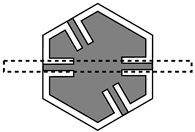
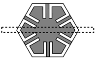
The method used to evaluate the UCPBG and HCPBG unit cells consists of a PCB having a microstrip line that crosses the entire top layer and one single cell at the bottom layer underneath the microstrip line.
Figure 1 illustrates a diagram used in this work for simulation and measurements. By supposing an interfering signal impinging the stripline, the objective here is to calculate a resonance frequency for the structure to filter out the interference.
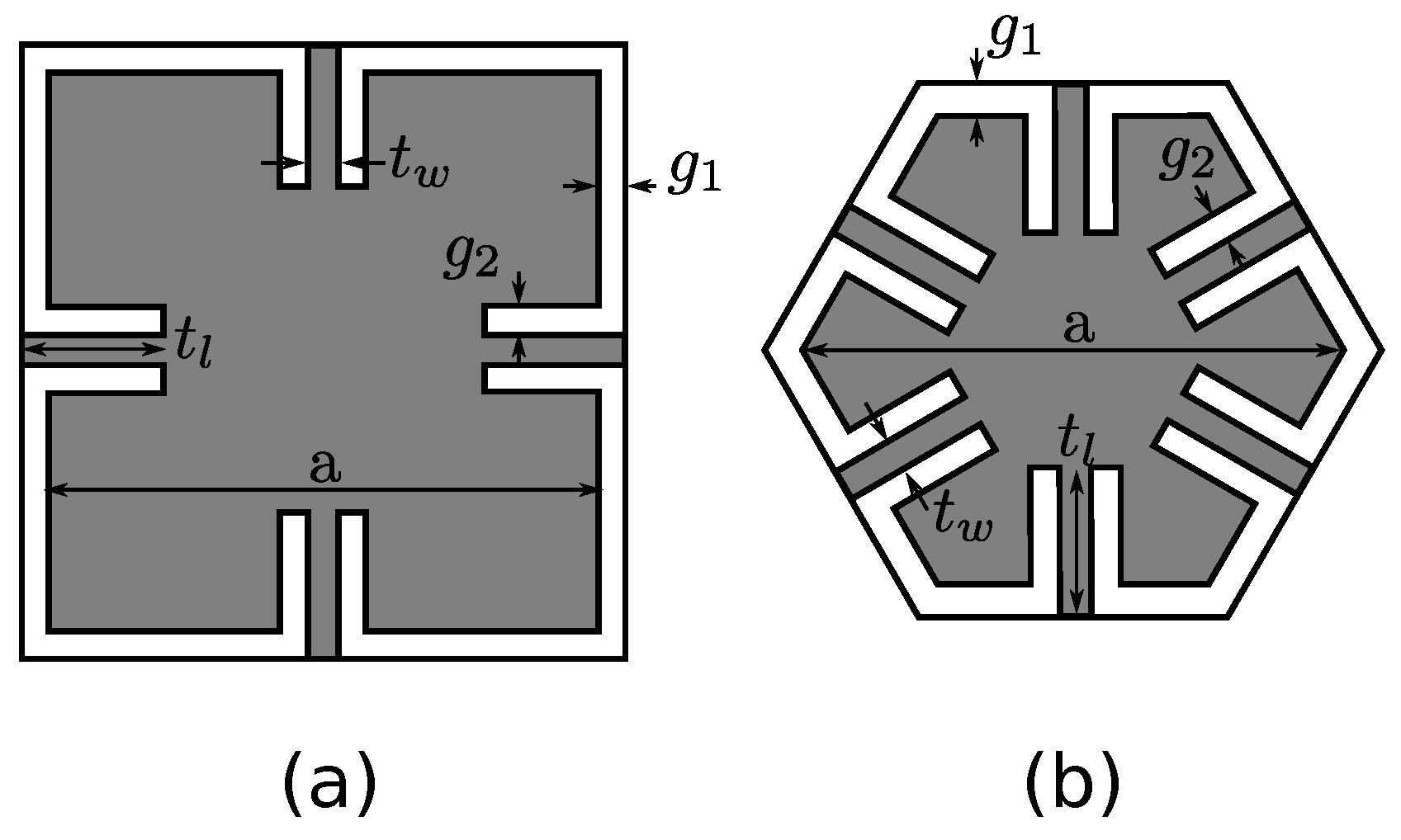
Figure 2 shows (a) the design reference UCPBG and (b) the new proposed HCPBG unit cells on microstrip substrates. The dark area is the metallic ground layer, while the white area represents the removal of the metal (air gaps). The geometry design parameters for both UCPBG and HCPBG are the gap size
,
, the total structure size
a, and the trace dimensions where
is the length and
is the width. The gap sizes define the capacitance, while the trace length and width define the inductance. For example, reducing the gap size
,
increases the capacitance and, henceforth, resonance moves to lower frequencies. On the other hand, a longer length
will produce a higher inductance, consequently reducing the rejection band frequency. Similarly, the width
affects the inductance and, henceforth, the resonance frequency.
The lumped capacitors and inductors introduced by gaps and traces form a parallel LC network as described in [
2]. The determination of a stopband frequency for a single PBG structure is roughly determined by [
5]
where
L is the inductance of the trace and
C is the capacitance of the gaps connecting the PBG structure to the ground. The method for calculating
C follows the model of two metal sheets coplanar capacitance on a PCB [
26], which can be calculated as
where
w is the size of the metal plates of the considered capacitor model,
(FR4) is the substrate dielectric constant,
c = 299,792,458 m/s is the vacuum speed of light, and
is the gap length. It is also convenient to make
to minimize the effect on the inductance
L.
One can calculate
L as [
27]
where
and
h is the substrate thickness.
The calculated values of
,
C, and
L define the dimensions considered in the EM simulations. It is also a starting point where the designer must proceed a fine-tune to achieve a desired resonance center frequency. Also, a second method one can use is scaling based on a predesigned structure. The rejection band moves to lower frequencies as the structure is scaled up and vice-versa. Furthermore, the attenuation further improves if the PBG structure forms a lattice. As the designer works at higher frequency ranges, UCPBG achieves smaller geometric sizes, improving its applicability. In this case, metal slots are etched in the ground plane connected by narrow lines to form a distributed LC network [
17]. This method fits well for standard PCB designs because it is planar, countering the need for vias or unique materials, saving costs. Concerning the hexagonal geometry, the reduction in the PCB-occupied area is the most attractive design feature. It can keep the same gap perimeter on the side of a square while occupying 65% of the area.
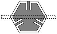
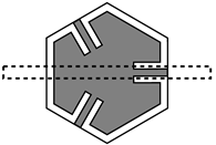
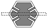
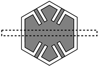
The current work investigates six variations of HCPBG geometries. The desired
is achieved by simply changing the number of traces, introducing different gap lengths, rotation of PBG structure relative to the microstrip line, and geometric scaling.
Table 1 describes and illustrates the variations proposed for simulations and measurements. Each line of the table constitutes the structure case, the number of traces, rotation, and the PCB bottom layer PBG structure relative to the microstrip line represented as dashed contours. The cases of
Table 1 (a) and (b) explores the asymmetry in the HCPBG structure by suppressing some of the traces, which changes the LC elements from the basic geometry presented in
Figure 2b.
The capacitance of the gap and the trace inductance closer to the point where the transmission line crosses the PBG have a more substantial influence on the resonance frequency. Adding asymmetry changes the values of the LC and the influence over the resonances.
The cases (a) and (b) are the three traces and show asymmetries for both gaps and traces close to the microstrip line. For cases (c) and (d), we can notice that traces and gaps are symmetrically apart from the microstrip line, and in case (e), there are two traces parallel to the microstrip line due to the rotation of 30°, for which it is expected to have similar results to the UCPBG. Finally, the case (f) is the fundamental geometry presented in
Figure 2b.
3. Simulation of HCPBG
The simulation setup consists of a reference plane PCB (without PBG on the ground layer), a UCPBG, and six HCPBG combinations shown in
Table 1. Six out of seven simulations on HCPBG structures have dimensions defined in
Table 2 case (a). The seventh simulation has dimensions defined in
Table 2 case (b), where
is the only different parameter. We calculated the PCB’s frequency profile using CST Studio
® [
28], an electromagnetic field simulation software.
In the CST Studio simulation, we set the time domain solver, which employs finite integration technique (FIT) [
29]. The time domain solver has the ability to handle large and complex structures, and it allows for memory efficient computation. We set the accuracy to −40 dB and hexahedral mesh type. For the mesh properties, we defined 12 cells per wavelength near/far from model and 35 cells of fraction minimum cell near model.
The PCB is an FR-4 two-layer of 90 mm length, 60 mm width, and 1.6 mm thickness. The microstrip line is 50
, 3 mm width and 90 mm length on the top layer. The ground plane is placed on the bottom side of the PCB, where the HCPBG and UCPBG structures are located, as shown in
Figure 1. The simulations consider the dimensions of
Table 2 case (a) where
nH,
pF and
GHz when using Equations (
2) and (
3). The nomenclature to name the HCPBG structures is defined as HCPBG-xx-yy, where “xx” represents the number of traces and “yy” is the orientation relative to the microstrip line.
The most significant characteristic of HCPBG unit cell is that multiple resonance profiles emerge due to rotation and trace suppression.
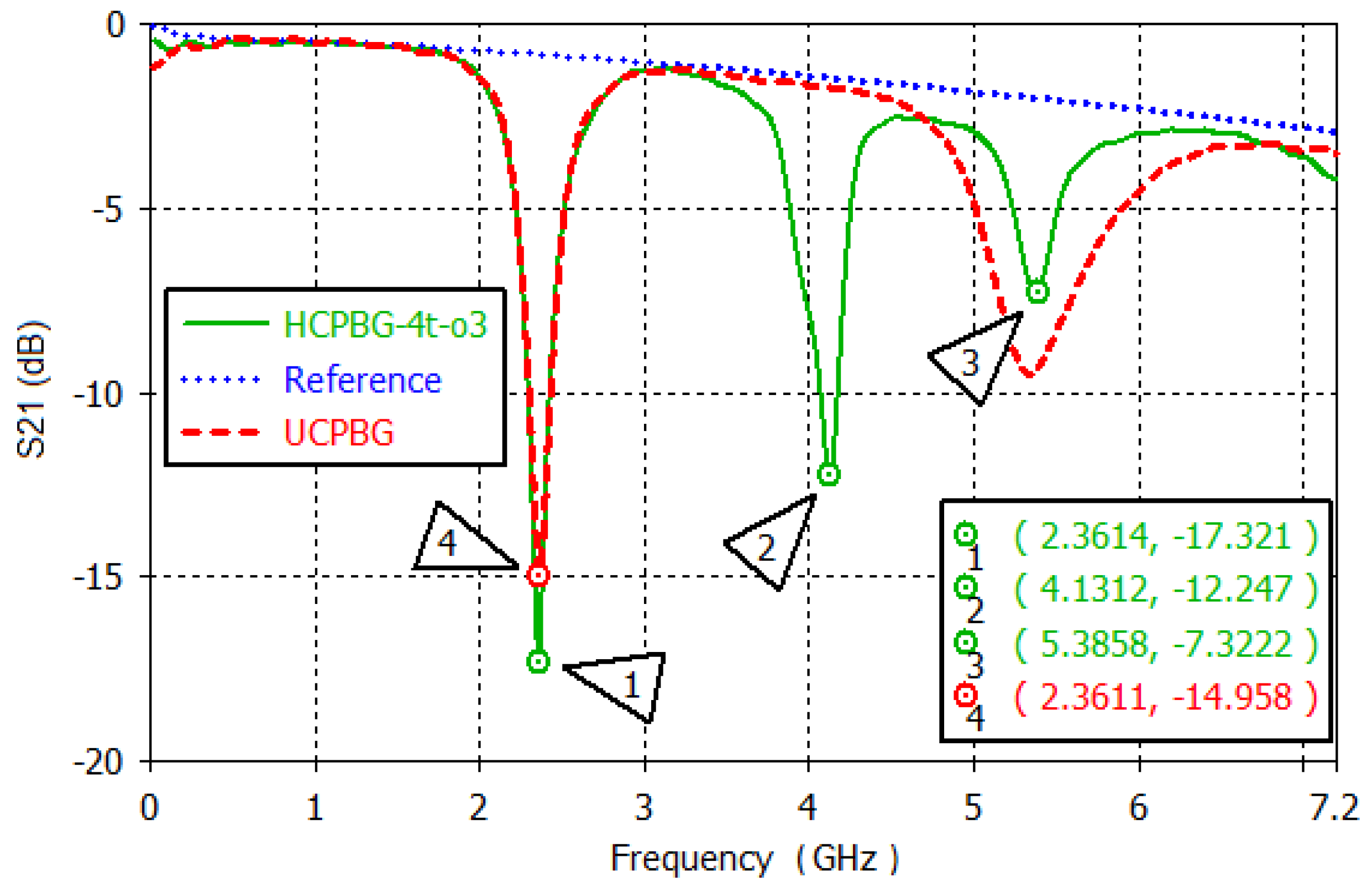
Figure 3 shows the transmission loss profile for UCPBG and HCPBG
Table 1 case (e). Both have similar results up to 3.3 GHz, with the first resonance at 2.36 GHz and similar bandwidth (BW); BW = 136 MHz at −10 dB. This case presents a second strong resonance at 4.13 GHz with BW = 100 MHz and the third one at 5.38 GHz, but with an attenuation lower than the −10 dB. This third resonance coincides with the second resonance of the UCPBG structure but with lower attenuation.
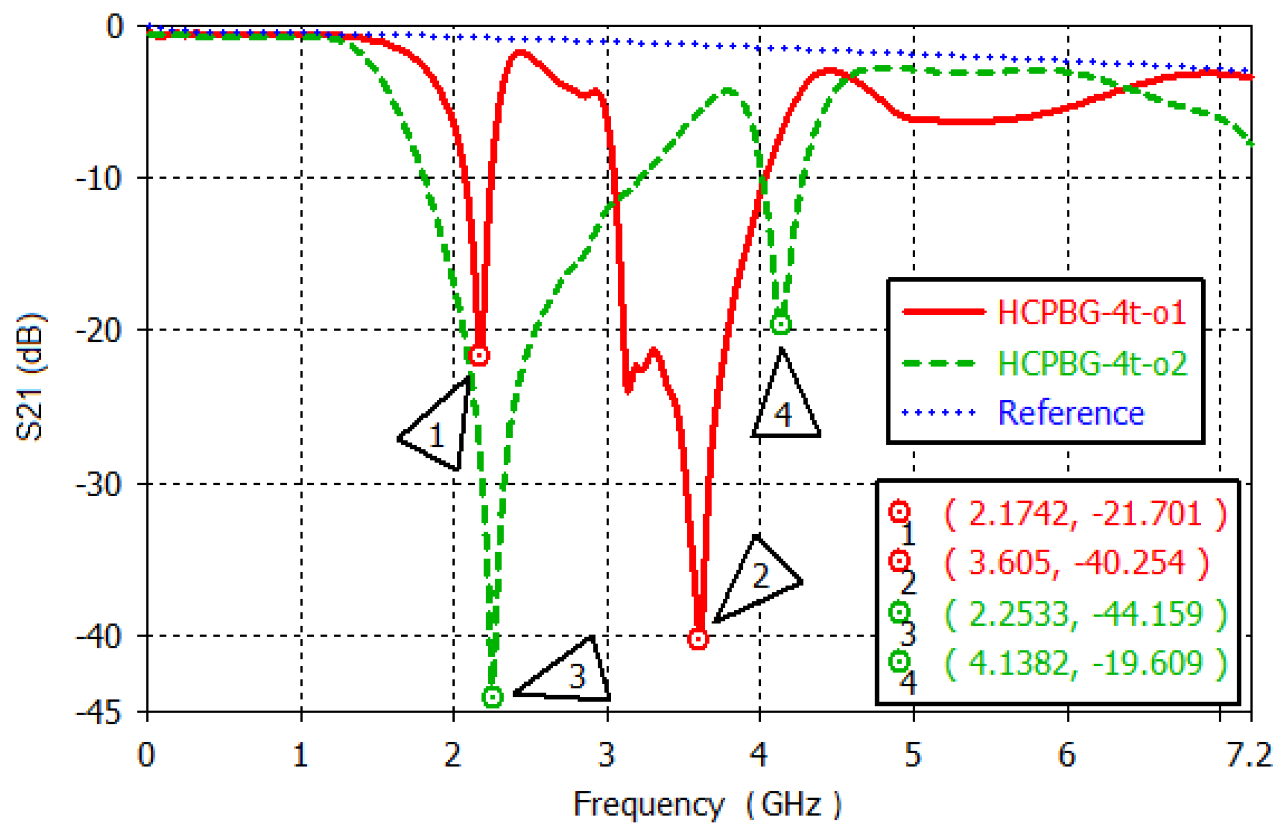
Figure 4 highlights the effect of HCPBG rotation for
Table 1 (c) and (d) cases. HCPBG and UCPBG present a similar filtering profile observed in the previous simulation. Notice that the main differences are due to the rotation of HCPBG-4t-o1 and HCPBG-4t-o2 (
Table 1 case (c) and (d), respectively). The HCPBG-4t-o1 has two strong attenuated bands, one at 2.17 GHz (BW = 167 MHz) and the second at 3.61 GHz, with a wide bandwidth (BW = 982 MHz). In HCPBG-4t-o2, the first attenuation band has an extensive bandwidth at 2.25 GHz (BW = 1.4 GHz), and the second resonance locates at 4.14 GHz (BW = 260 MHz).
We also simulated HCPBG with three traces and six traces, keeping the same dimensions to verify the attenuation band profile’s behavior.
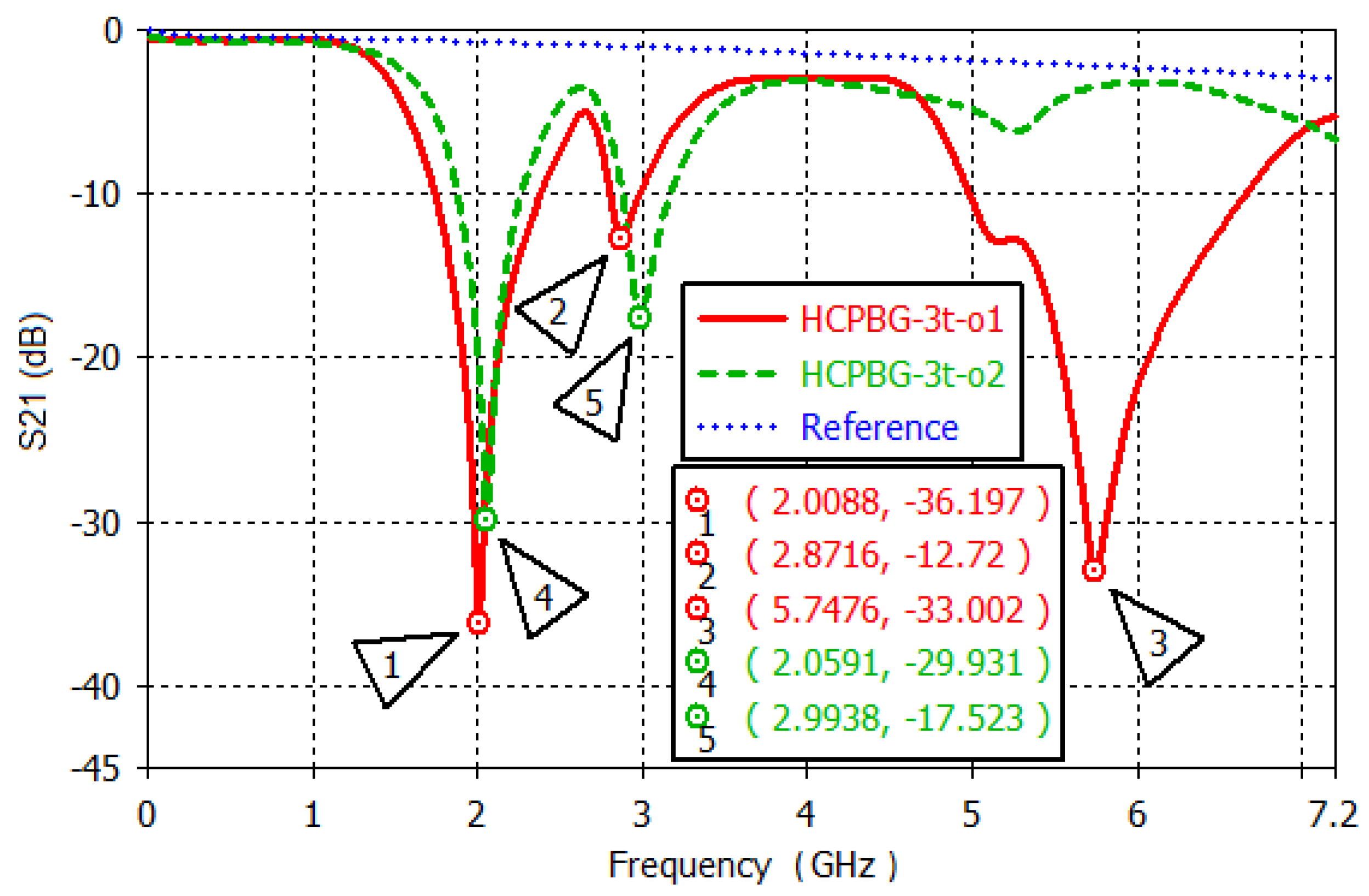
Figure 5 shows the transmission loss for the HCPBG with 3 traces and two different orientations, as indicated in
Table 1 by cases (a) and (b). Both have similar filtering profiles up to 4.5 GHz, with a first attenuation around 2 GHz, and with BW of 645 MHz for HCPBG-3t-01 and BW of 380 MHz HCPBG-3t-o2. The second attenuation band is close to 3 GHz for both. The main difference is that HCPBG-3t-o1 produces a third strong wideband attenuation at 5.75 MHz (BW = 1670 MHz). The LC network seen by the microstrip line depends on the HCPBG orientation, and it seems to have more impact when the HCPBG traces are more aligned with the microstrip line.
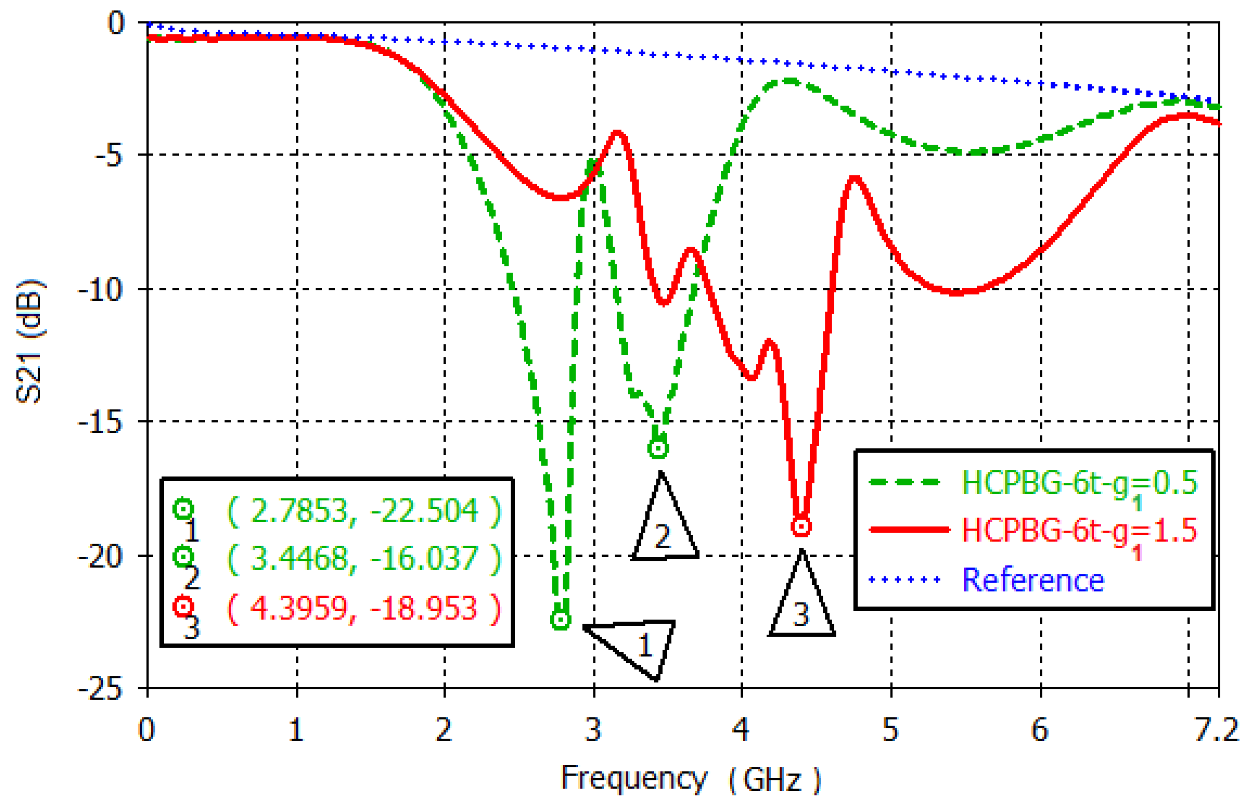
Figure 6 shows the transmission loss simulation results for the 6-trace HCPBG,
Table 1 case (f), with outer gaps of 1.5 and 0.5 mm. A smaller gap results in a greater capacitance, leading to lower rejection band frequencies. The HCPBG-6t with a gap of 1.5 mm has a significant bandwidth response if we use a criterion of −5.8 dB (BW = 3.16 GHz). This structure could be helpful in the suppression of broadband noise.
4. Measurements of HCPBG
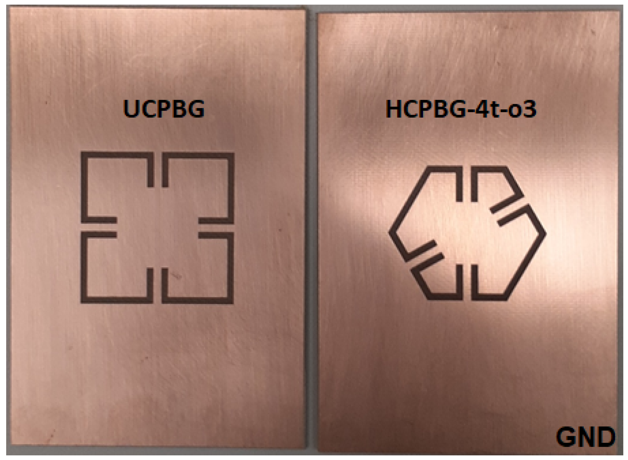
We also verified the analytical guidelines and simulation results performing measurements in an actual PCB. An LPKF machine milled the 2-layer FR-4 samples of UCPBG and HCPBG structures.
Figure 7 shows the bottom side of two fabricated samples, UCPBG (to the left) and the HCPBG-4t-o3 (to the right). The HCPBG-3t-o1, HCPBG-3t-o2, HCPBG-6t (g = 1.5 mm), and the reference board (ground only) were also fabricated. The sample dimensions and substrates are the same used for the simulations.
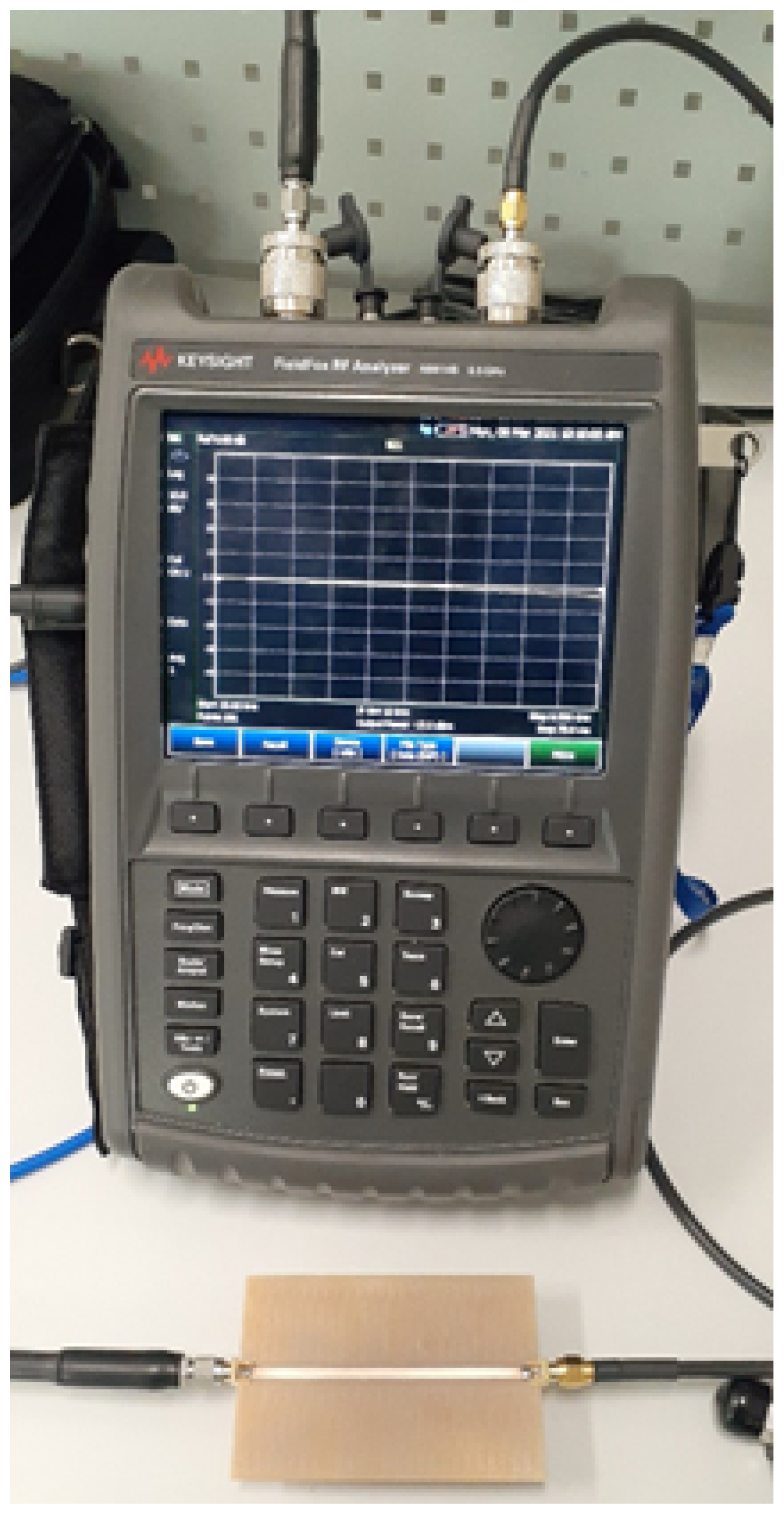
The measurement setup, shown in
Figure 8, is composed of the Keysight Field Fox RF Analyzer N9914B, 2 RF cables, N-SMA adapters, and the samples. The analyzer is set to network analyzer mode and calibrated from 30 kHz to 6.5 GHz.
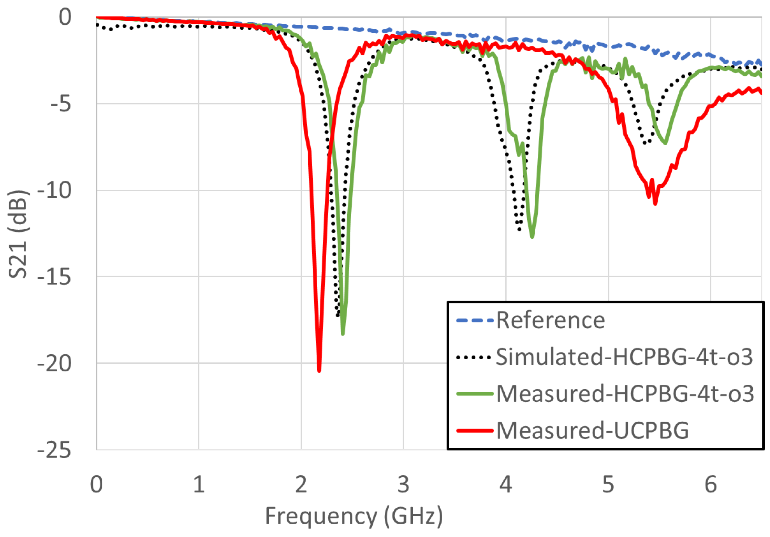
The measured logarithmic magnitude of S21 parameter for the UCPBG and HCPBG-4t-o3 can be seen in
Figure 9. When comparing the results in
Figure 3, we can observe that the simulation curves’ profiles are very close to the measurement results. However, the resonance frequencies showed a slight discrepancy, with the UCPBG’s case being the more evident one. This discrepancy is probably due to fabrication process variations, such as gap width, depth, and substrate dielectric constant variation. Nonetheless, the simulation results showed good accuracy that can be observed in all measurements. The UCPBG’s measured first resonance frequency is at 2.18 GHz (BW = 160 MHz), and the second one at 5.4 GHz. For the HCPBG-4t-o3, the resonance frequencies are 2.4 MHz (BW = 160 MHz), 4.26 GHz (BW = 130 MHz), and 5.56 GHz. The bandwidth and maximum attenuation are also very similar in both measurement and simulation. The reference line represents the measured S21 for the transmission line with a solid ground plane (no PBG).
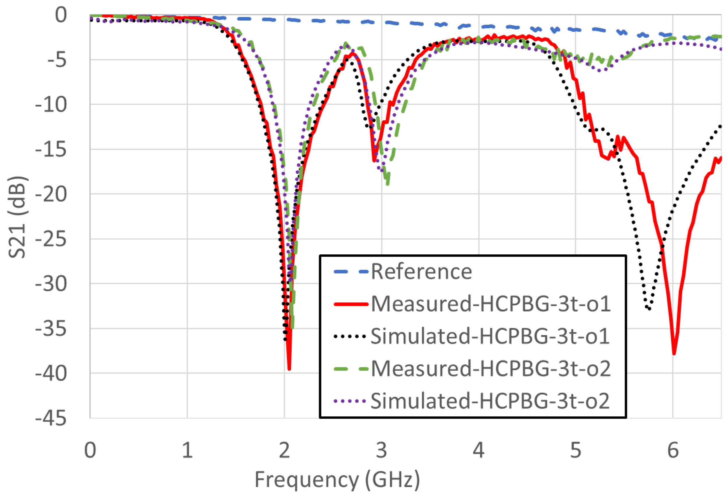
The graphics of
Figure 10 show the measurement results for the three trace geometries: HCPBG-3t-o1 and HCPBG-3t-o2. The simulation results are in good accordance with the measurements concerning curve profile, rejection band center frequency, and bandwidth. Similarly to the simulation, the HCPBG-3t-o1 first attenuation band is at 2.04 GHz (BW = 650 MHz), and for HCPBG-3t-o2, it is at 2.08 GHz (BW = 390 MHz). The second resonance appears at 2.92 GHz (BW = 260 MHz) and 3.05 GHz (BW = 292 MHz) for orientations 1 and 2, respectively. Also, as predicted by simulation, a third wide resonance occurs at 6.01 GHz (BW = 1.4 GHz) for the case of HCPBG-3t-o1.
Finally,
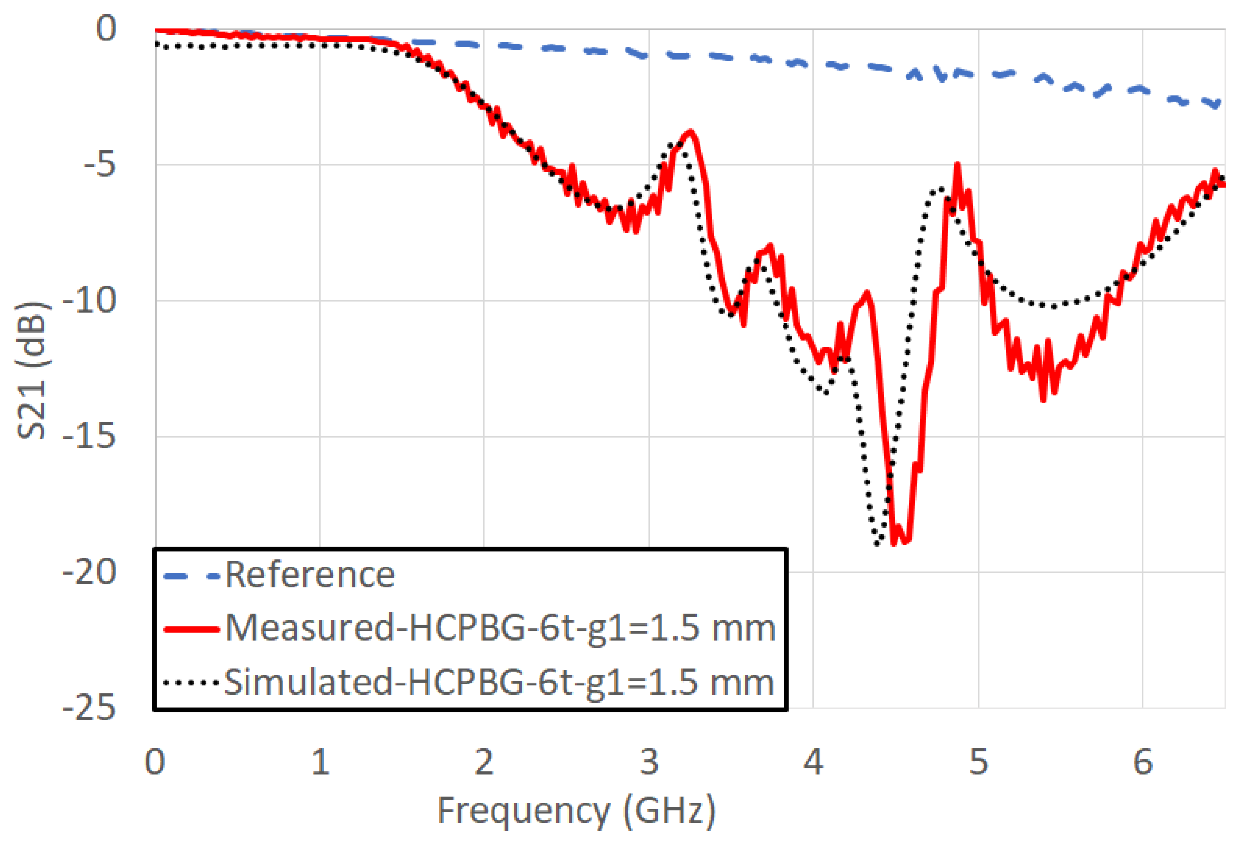
Figure 11 shows the transmission loss measurement results for the six trace HCPBG with a gap of 1.5 mm. Although it shows a significant bandwidth response and a similar profile, when compared to that of the simulated model, the bandwidth is reduced when we use −5.8 dB criteria. To have similar bandwidth, the criteria would need to be around −5 dB. The more substantial attenuation is at 4.55 GHz (−18.8 dB).
The simulation results show an error of less than 2% in the resonance frequencies below 4 GHz, while for values above 4 GHz, the error is less than 4%. The discrepancy between the measurements and simulation results for higher frequencies could be due to a mismatch between the dielectric characteristics of the PCB and the simulation model, over frequency. The variations in the fabrication process of the board would also impact the structure geometry; for example, changing the gap capacitance and displacing the resonance frequency.
5. Design of Reconfigurable HCPBG
First, it is essential to remind that the central concept of HCPBG concerns the model of two metal plates separated by gaps of etched copper. Also, the traces of each hexagon face and gaps define the features of an equivalent LC network. Then, it is possible to tune the resonance center frequency of the filter by actively controlling the parameters L and C. The simplest method to achieve frequency tuning is to switch on/off one or more traces that result in inductance changes. For this purpose, it is possible to use FET transistors or micro-electro-mechanical systems (MEMS) switches. The caveat of this approach is the additional capacitance of the FET transistor or MEMS while in an off state, making the implementation more complex.
On the other hand, it is also possible to change the LC network using a variable capacitor at the gaps close to the transmission line. The technique allows actively reconfigure the first resonance frequency adding parallel capacitance to the overall intrinsic gap capacitance. In this case, a varactor diode connected to a bias tee circuit with a port connected to a DC voltage supply allows controlling the capacitance. The varactor diode method is less complex than active inductor circuits or RF switches and provides fine-tuning of the first resonance frequency. Hence, the cost of implementing switches or the complexity of polarizing FET transistors for each trace of the HCPBG would be higher than using two varactor diodes to change the capacitance.
The selected HCPBG model for the reconfiguration study is the 6-trace type, and it can be observed in
Table 1 case (f). The main dimensions used to create the reconfigurable HCPBG structure can be seen in
Table 3.
The model shown in
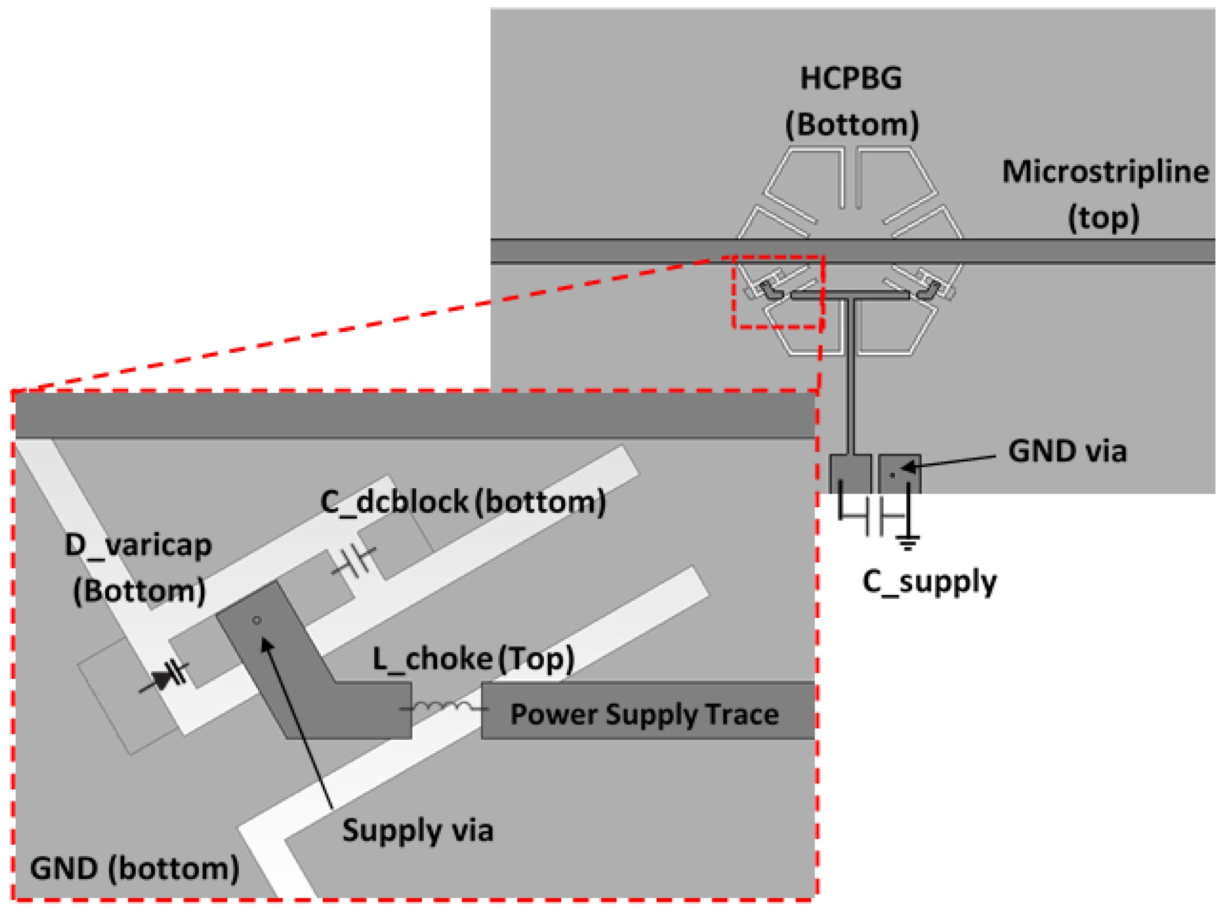
Figure 12 was simulated in the CST studio software. It consists of a 50
microstrip line on a 2-layer FR4 PCB, with a dielectric constant of 4.3, length of 90 mm, a width of 60 mm, and thickness of 1.6 mm. The ground plane is placed on the bottom side of the PCB, where the HCPBG structure is also etched. All pads, traces, and vias are designed to emulate the fabricated board.
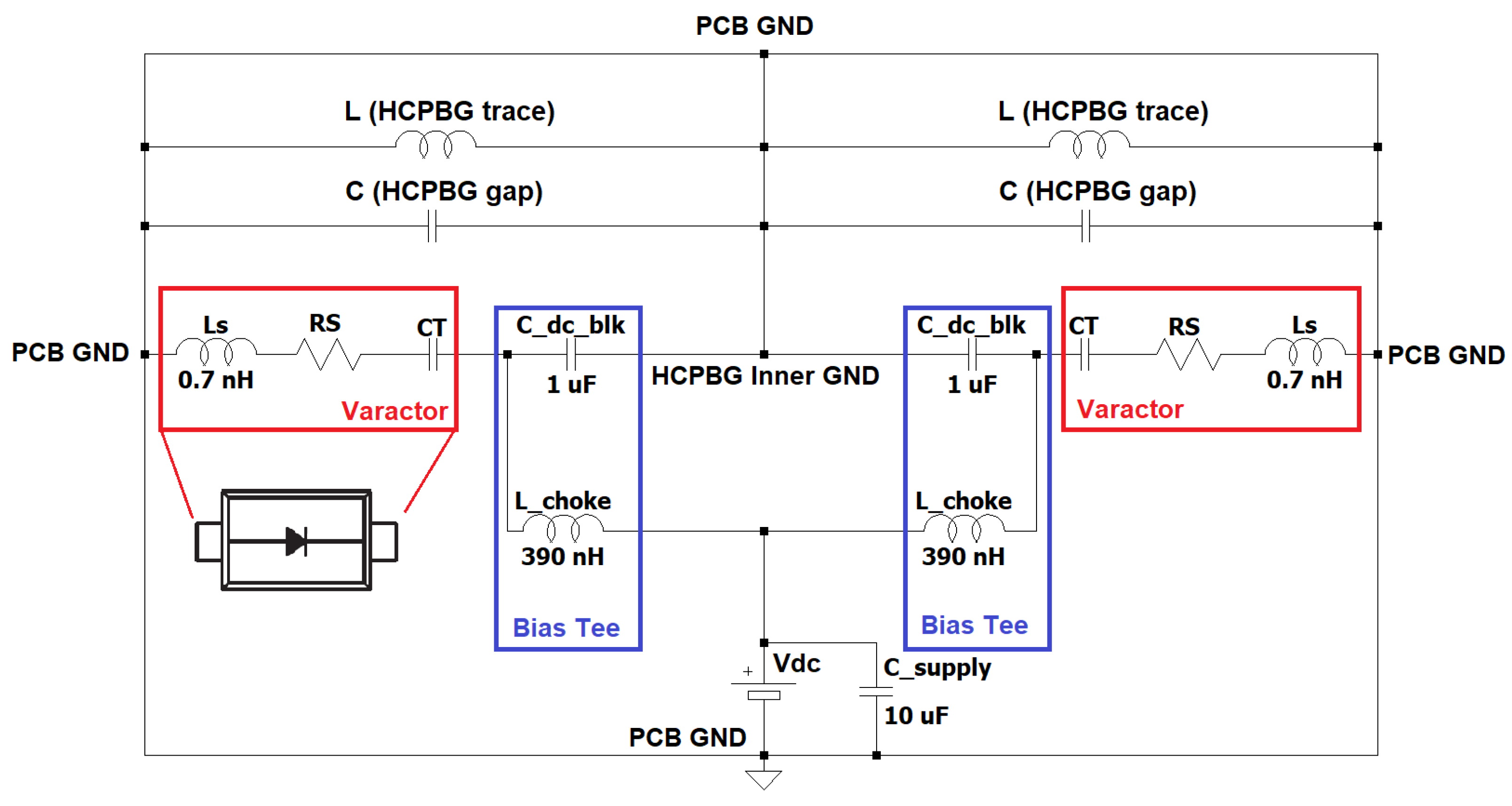
On the bottom layer, we have the varactor diode () and the DC block capacitor (). The inductor () to isolate the DC from the AC part of the circuit is placed on the top layer. A metal via connects the DC power supply traces from the top layer to the varactor on the bottom layer. At the end of the DC power supply trace, a capacitor () is connected to the ground to represent the power supply’s capacitive coupling to the common ground.
A simplified series RLC varactor model is used in the simulation. It is composed of a capacitor (
) in series with the parasitic inductance (
) and resistance (
). According to the datasheet of SMV1247 from Skyworks,
is 0.7 nH for the SC-79 package, and
is dependent on the applied reverse voltage (
), having a value that ranges from 2.5 to 9
. The applied reverse voltage controls the varactor’s capacitance (
). The rationale behind the choice of the SM1247 is that its capacitance range is in the same order as the gap capacitance of the HCPBG, giving a good dynamic range for frequency shifting.
Table 4 shows selected
versus
used for the simulations.
The representation of the varactor’s circuit model (
,
,
) and bias circuit electrical connections can be seen in
Figure 13. The varactor’s anode is connected to a common ground plane (PCB GND) and the cathode to the DC block capacitor (
), which is also connected to the HCPBG’s inner GND. This configuration allows DC bias isolation from the RF ground, for the
works as a second DC block element. Completing the bias tee, the inductor (
) isolates the RF signal from the DC power supply line. The DC power supply coupling capacitance (
) connects the DC line to the PCB GND.
The discrete component values used in the simulation can be seen in
Table 5.
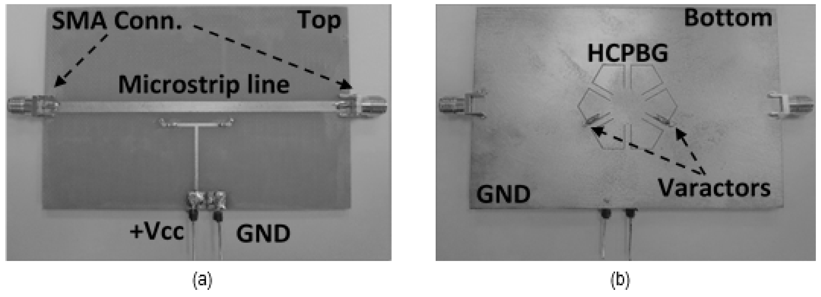
To validate the simulation model, we fabricated the testing sample using an LPKF milling machine. In
Figure 14a, is the top view of the fabricated sample, showing the microstrip line, SMA connectors, choke inductors, and DC power supply traces and pads. The bottom side of the sample is shown in
Figure 14b, containing the GND plane, HCPBG, varactor diodes, and DC block capacitors.
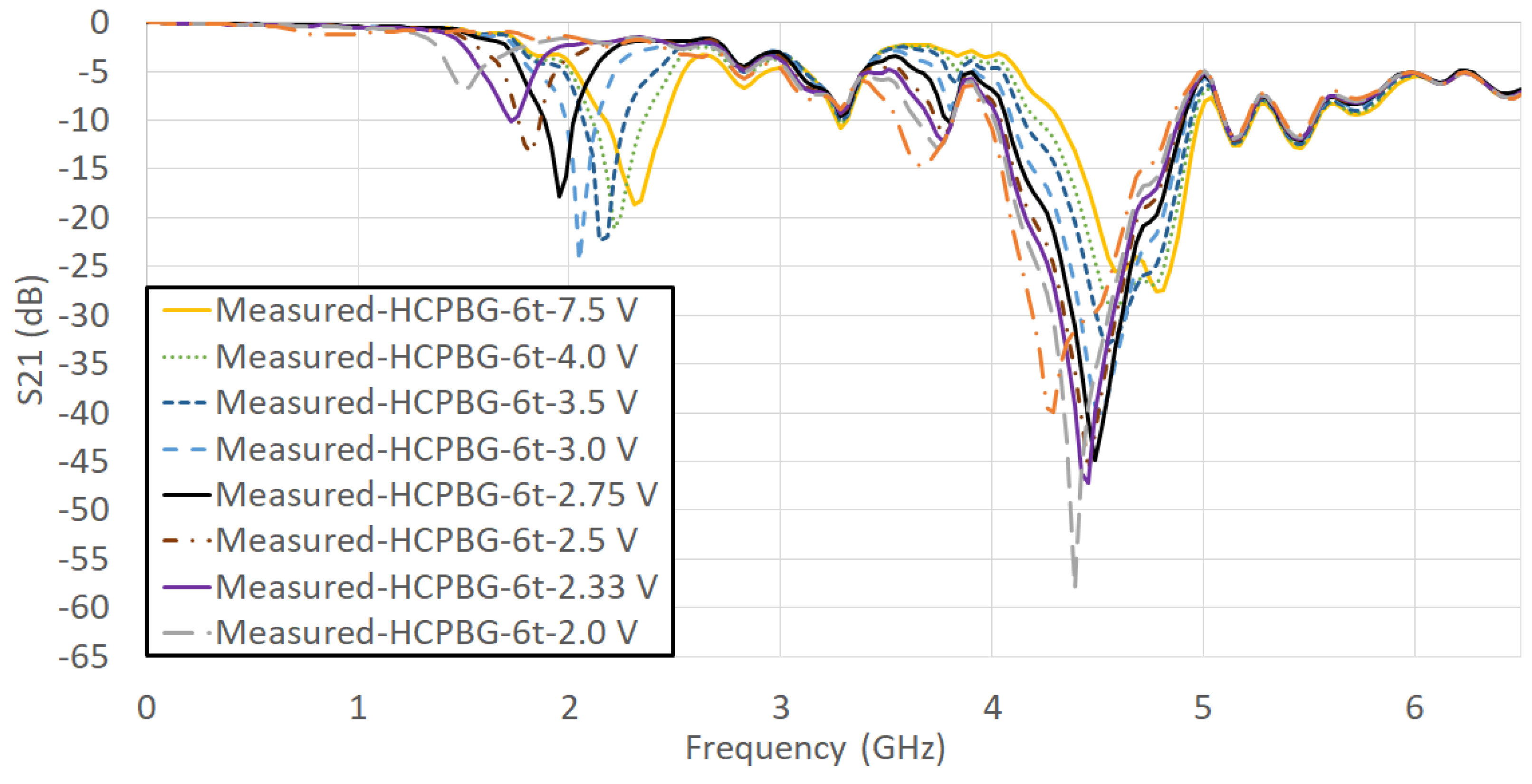
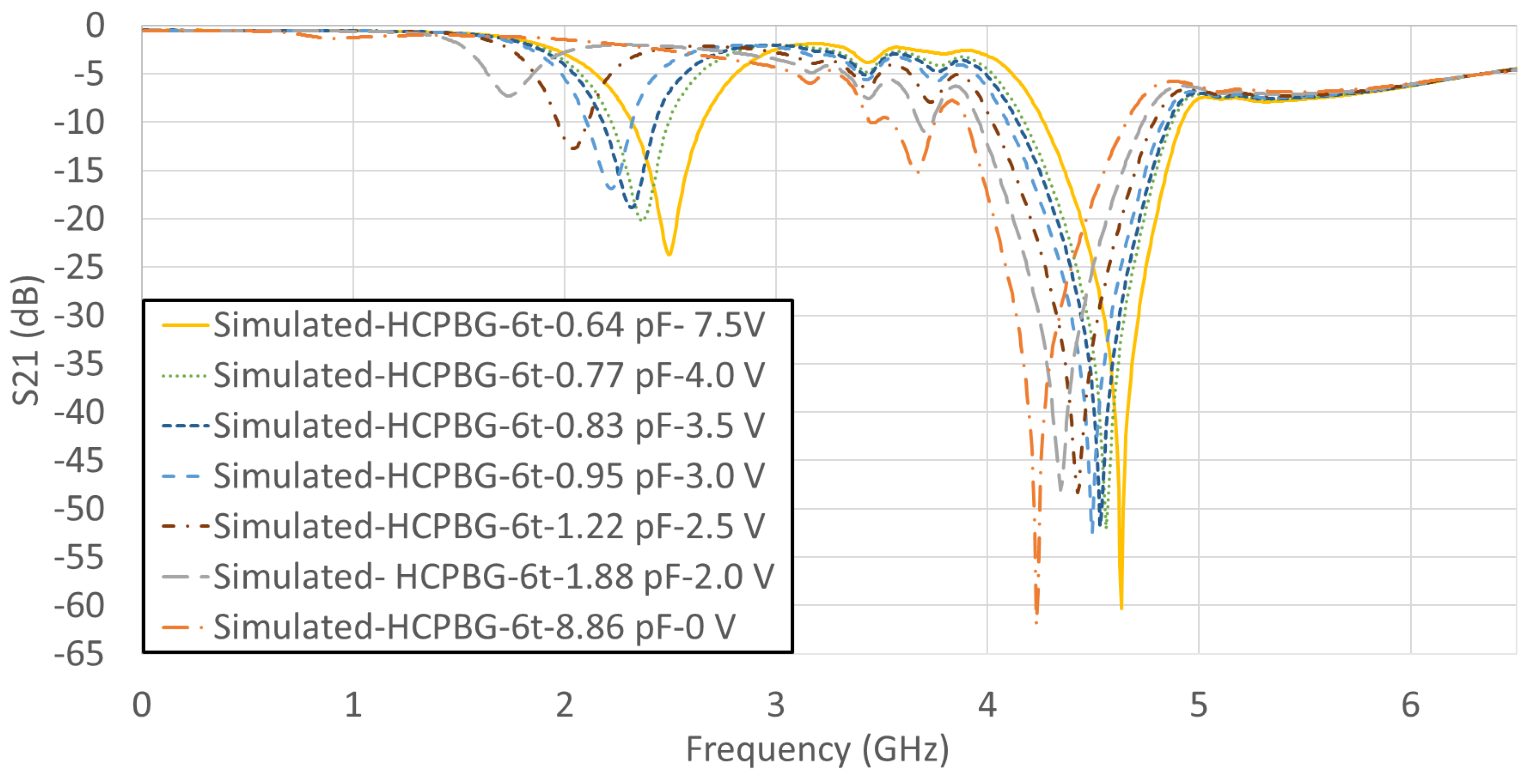
The filtering characteristic of the reconfigurable HCPBG can be observed by the simulated and measured transmission loss (S21) in
Figure 15 and
Figure 16, respectively.
Table 6 and
Table 7 show the simulated and measured resonance frequencies and bandwidths for different
or
values.
Both results show similar curve profiles, and reasonable approximation with respect to resonance center frequency and bandwidth. For instance, considering of 0.64 pF ( = 7.5 V), the simulated first resonance frequency is 2.49 GHz ( = 331 MHz) and the measured is 2.31 GHz ( = 260 MHz).
Starting the analysis with the simulation results, as we apply the lowest value (0.64 pF) two main resonances occur, the first one at 2.49 GHz ( = 331 MHz) and the second one at 4.63 GHz ( = 647 MHz). As expected, when we increase , the resonance frequencies are shifted to lower values. For example, if we take values of 0.83 pF and 0.95 pF, is displaced by 100 MHz to 2.32 GHz ( = 244 MHz) and 2.22 GHz ( = 209 MHz), respectively. The same behavior is observed for the measurement results; for example, for of 3.5 V (0.83 pF) and 3.0 V (0.95 pF), the is displaced by 70 MHz, going from 2.15 GHz ( = 160 MHz) to 2.08 GHz ( = 160 MHz).
The difference between the simulated and measured resonance frequencies is dependent on the varactor’s bias voltage or the selected . Considering values of 1.22 pF and above, the first resonance frequency showed an error of 15%. On the other hand, for capacitance values of 0.95 pF and bellow, the difference is less than 8%. According to the datasheet, the varactor SMV1247 can show 7% to 11% variation in the capacitance, depending on the applied voltage. Added to that, we have the fabrication process and substrate dielectric variations. For the second resonance, around 4.5 GHz, for which the varactor does not play a strong influence, the error is only 3%.
Another observed characteristic is the bandwidth and maximum attenuation reduction, as the resonance is shifted to lower frequencies. This reduction is strongly influenced by the varactor’s . For example, considering of 0.77 pF, then is 3.9 and simulated S21 equals to −20 dB @ 2.36 GHz. For of 1.22 pF, then = 6.3 and simulated S21 equals to −12.6 dB @ 2.02 GHz. Due to effect, the −10 dB criteria can not be achieved for 1.88 pF (S21 = −7.29 dB @ 1.73 GHz) and 8.86 pF (S21 = −1.35 dB @ 0.98 GHz), limiting the dynamic range of the reconfigurable filter. The measurement results confirm this characteristic. When we set to 2.0 V, or equivalently, to 1.88 pF, the filter attenuation stays above the −10 dB criteria (S21 = −6.97 dB @ 1.5 GHz). If we remove from the simulation, the bandwidth is also reduced as the frequency shifts, however the entire range of achieves the −10 dB attenuation criteria.
has a stronger influence over the first resonance frequency. For example, in
Table 6, if we observe the resonance frequencies at 0.64 pF and 8.86 pF,
shifts 1.51 GHz, however, the second resonance (
) shifts only 400 MHz.
For a −10 dB criteria, the measurements show a filtering capability that ranges from 1.72 GHz ( = 2.33 V) to 2.44 GHz ( = 7.5 V, upper band of = 2.31 GHz), that is 720 MHz bandwidth coverage.


 and
and 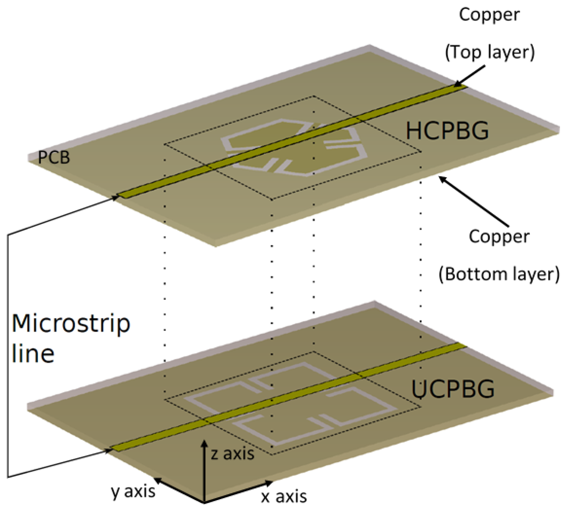


