
Towards Realization of a Low-Voltage Class-AB VCII with High Current Drive Capability


Abstract
:1. Introduction
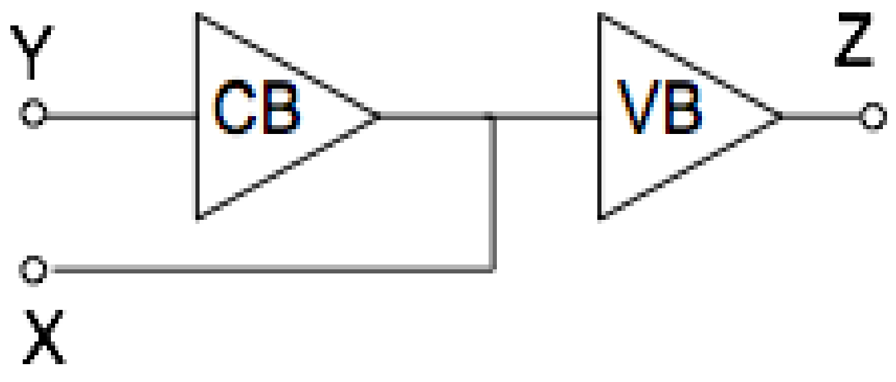
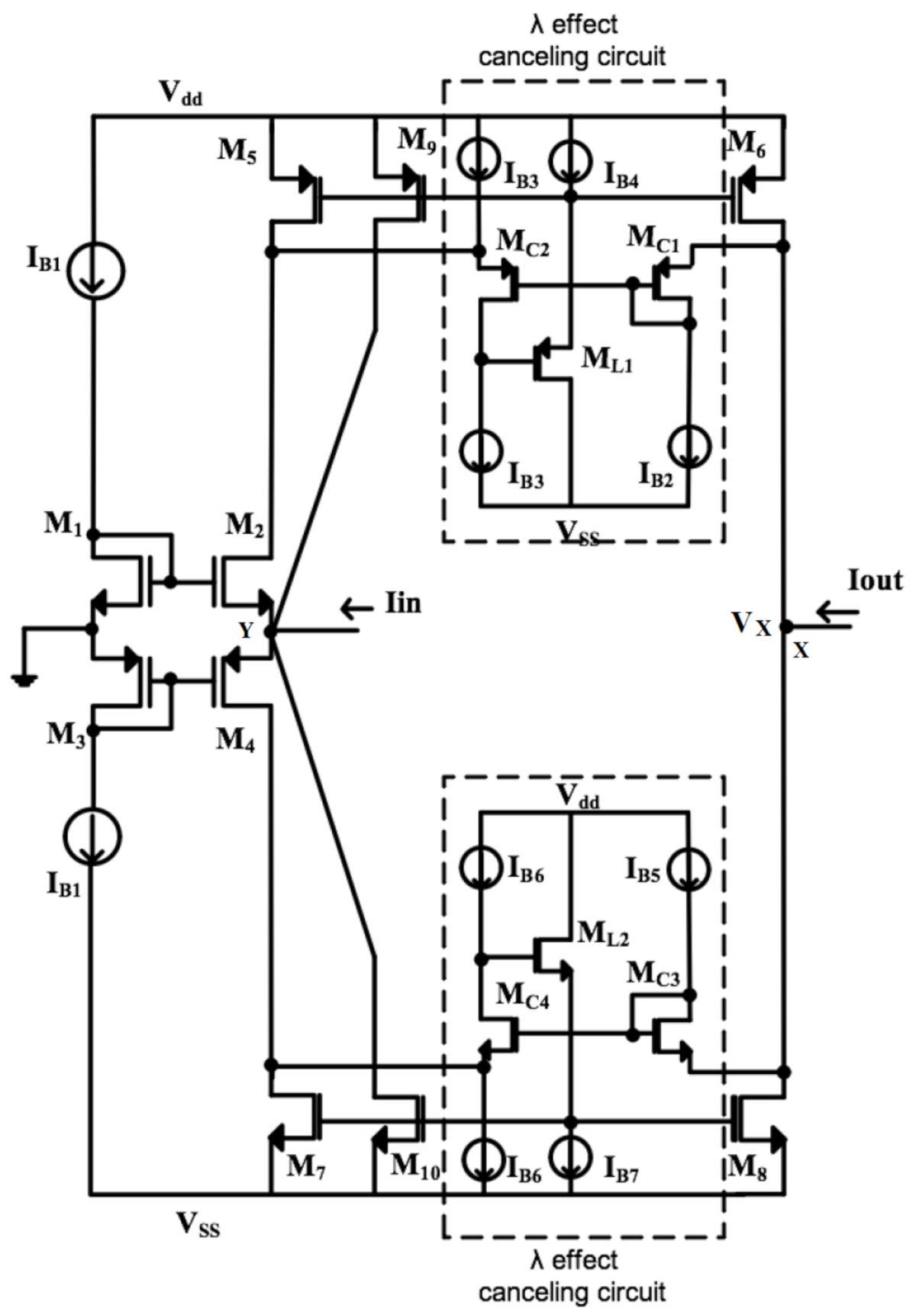
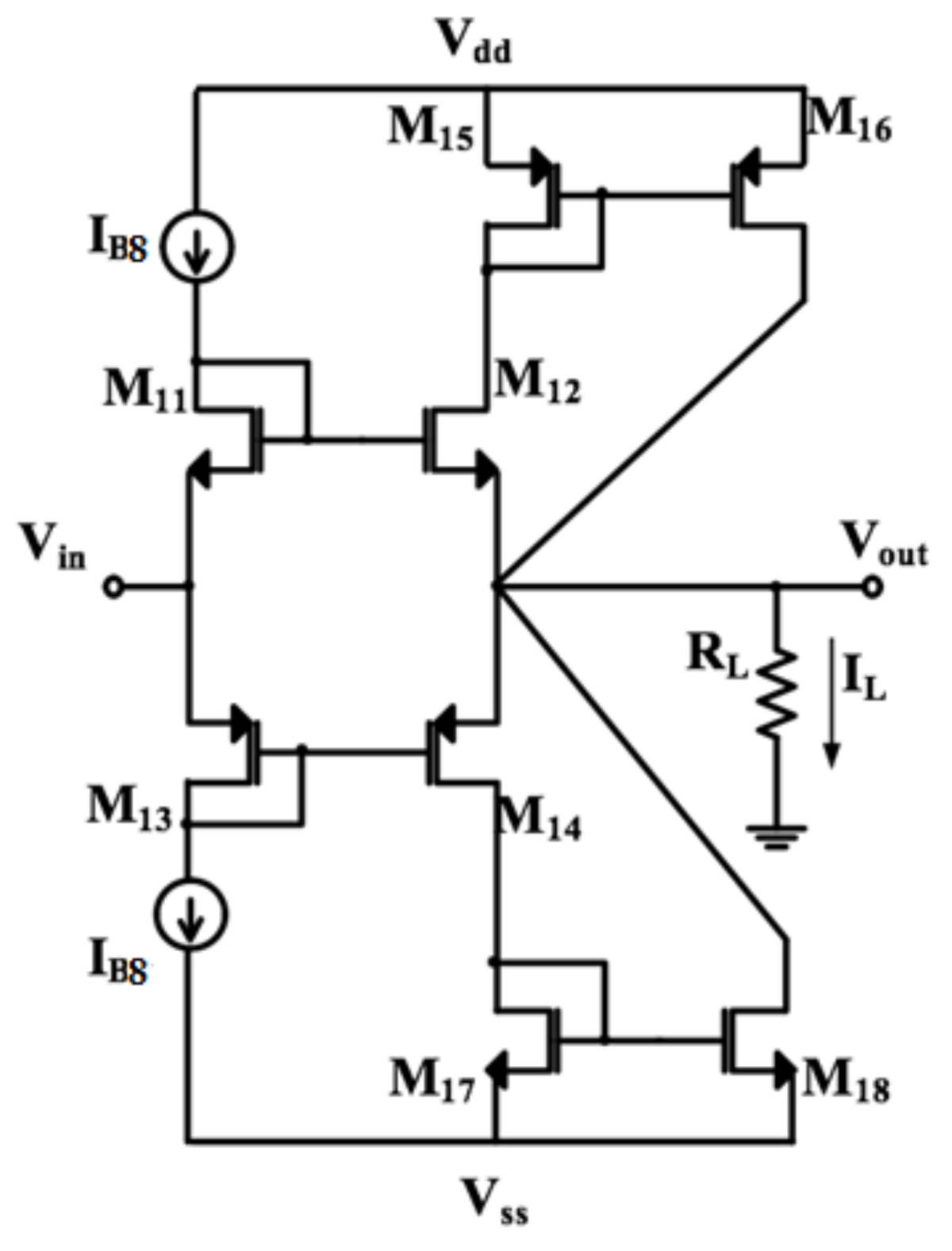
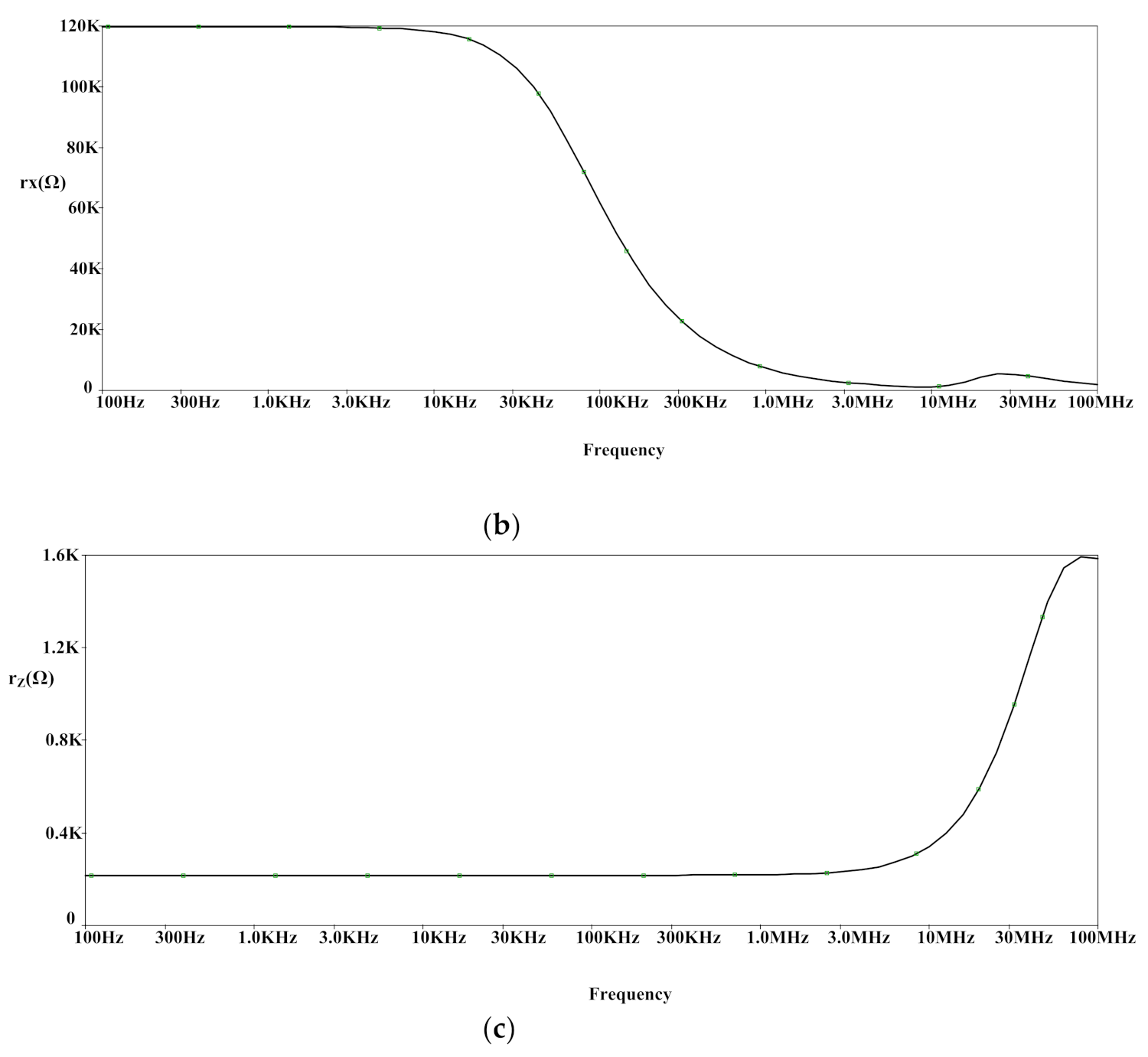
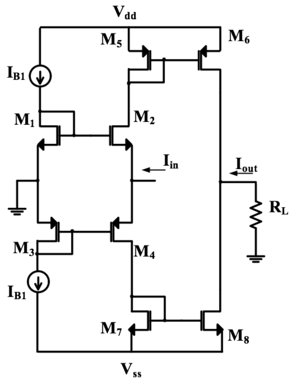
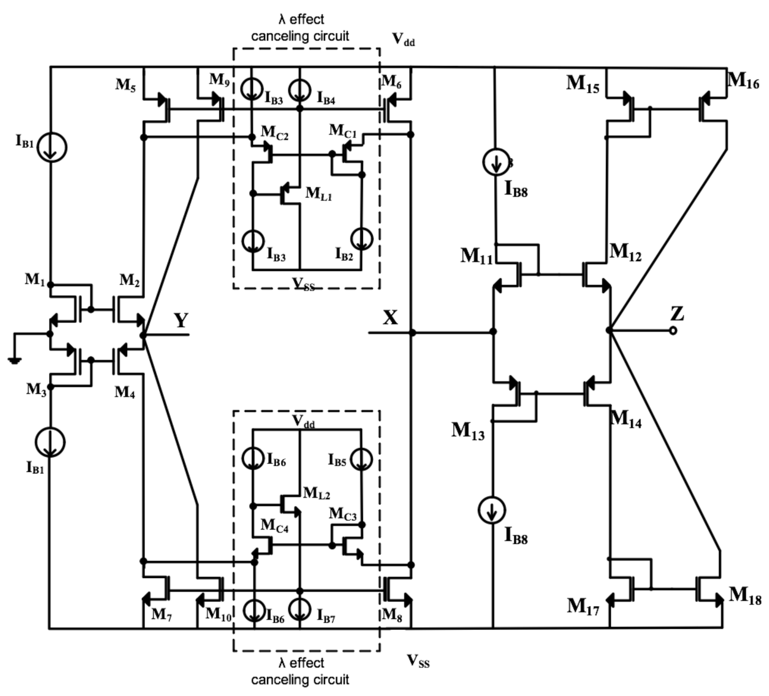
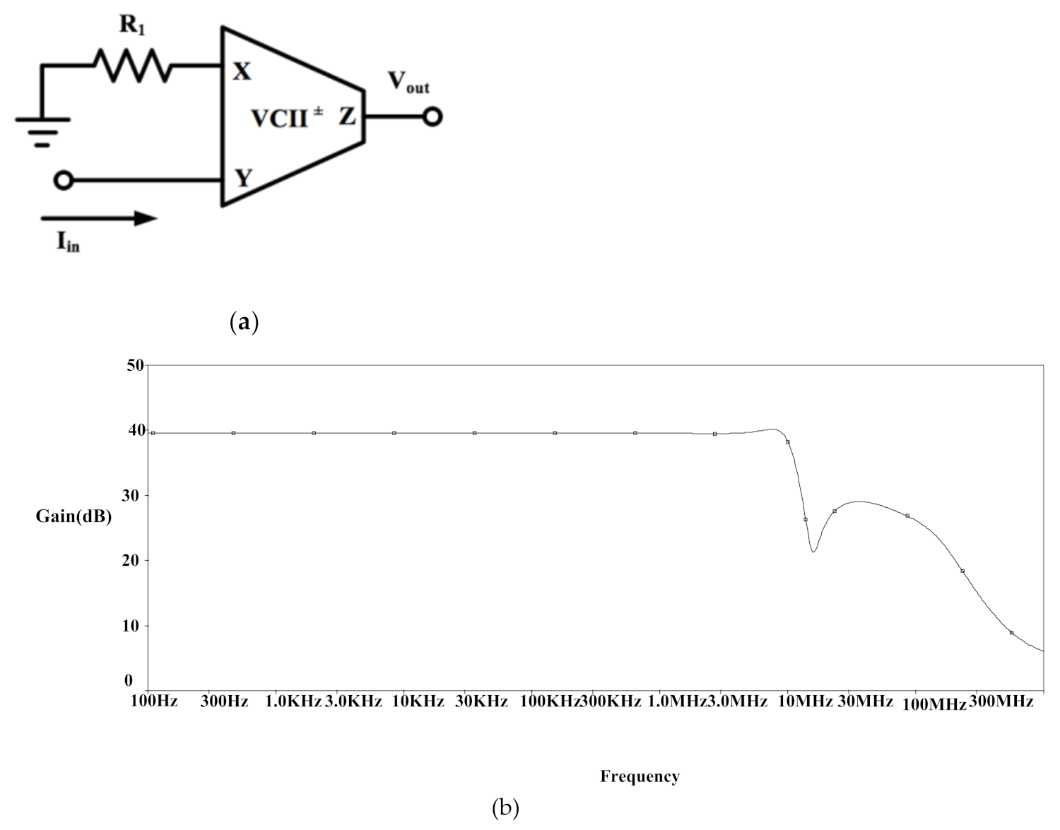
2. Class AB VCII Realization
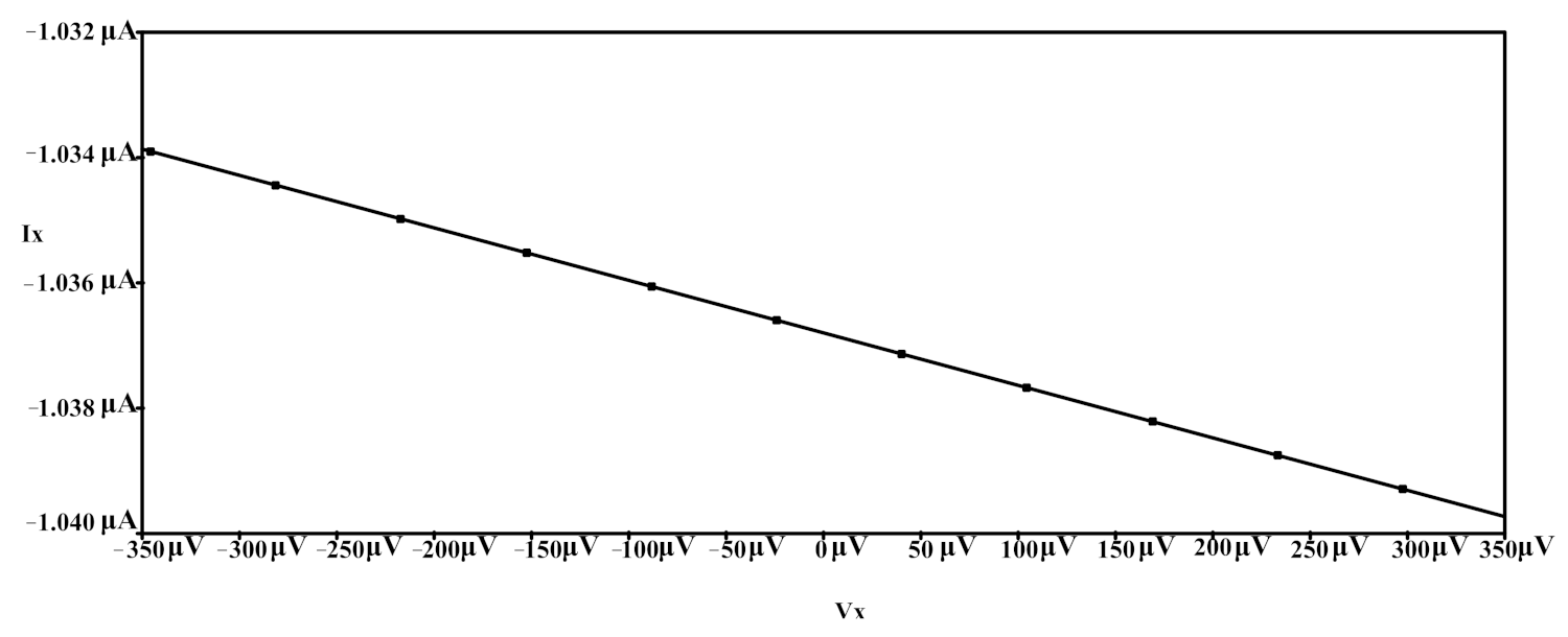
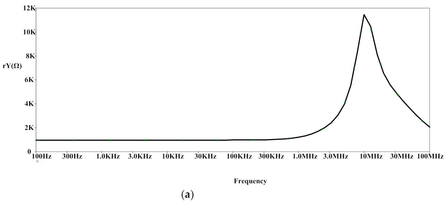
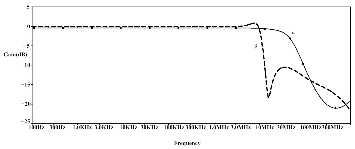
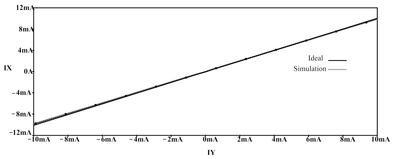
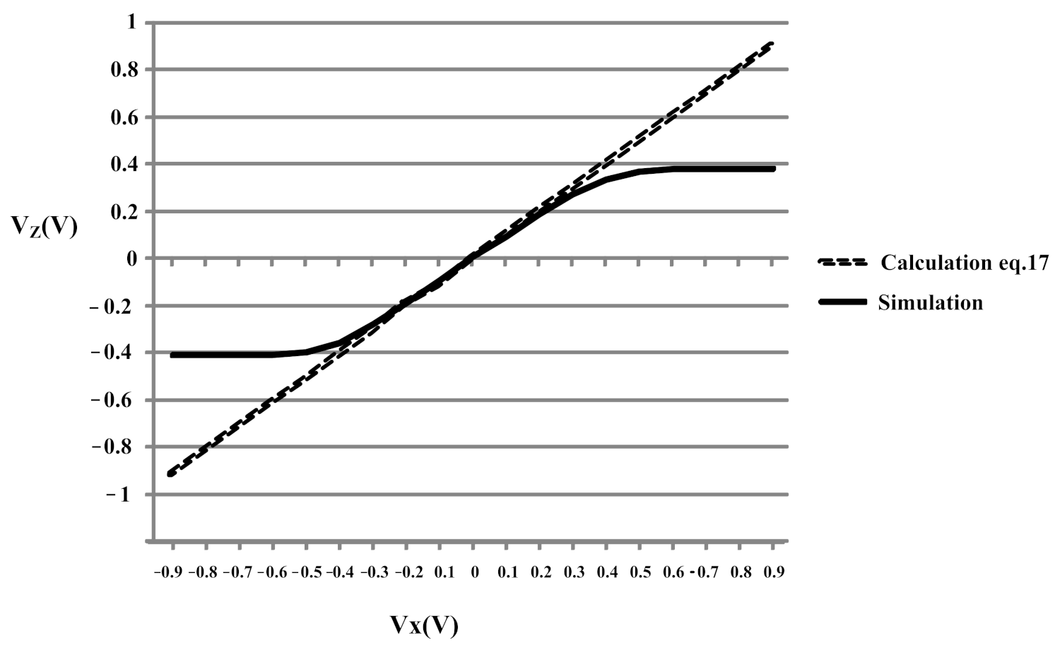
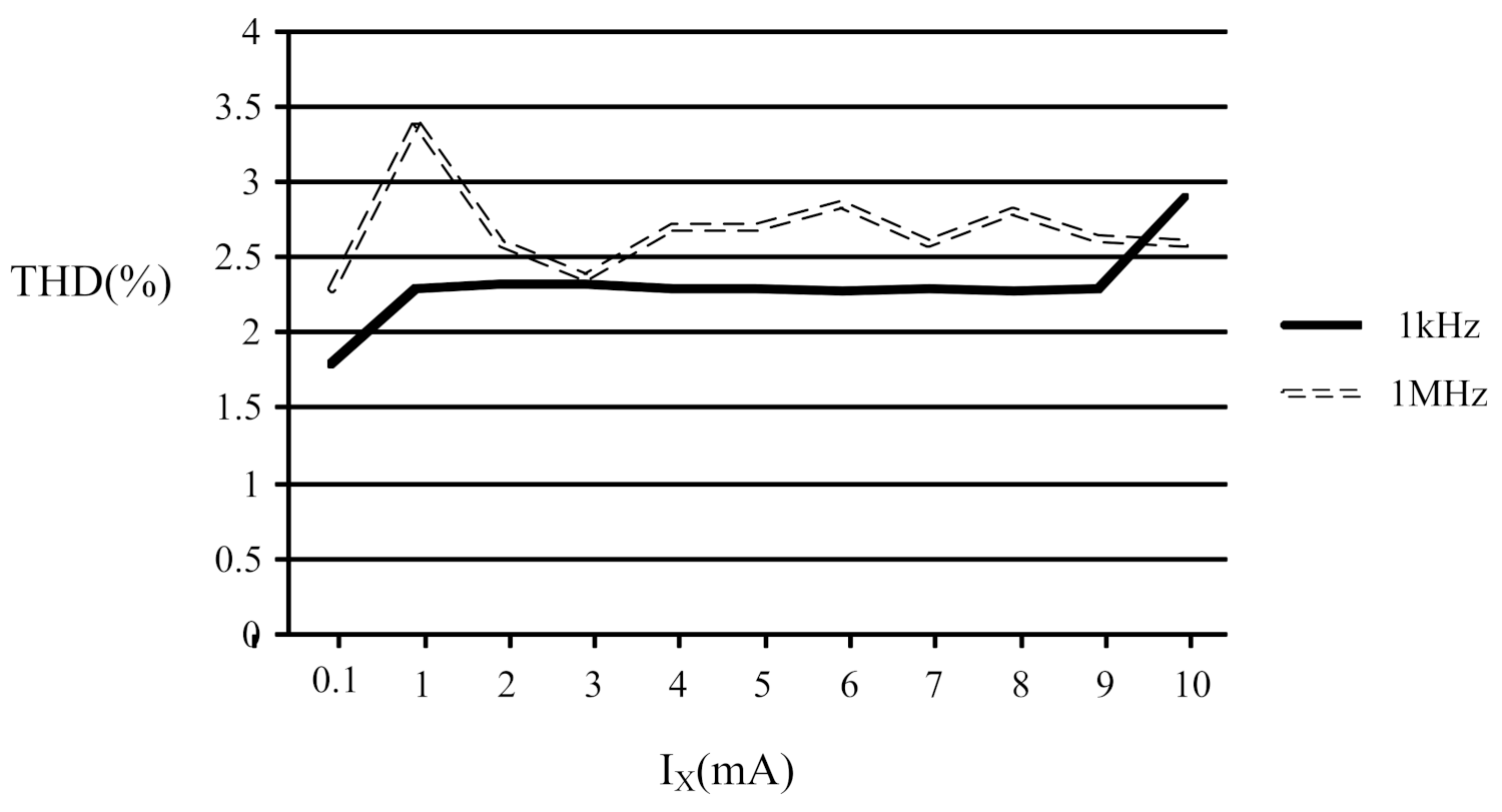
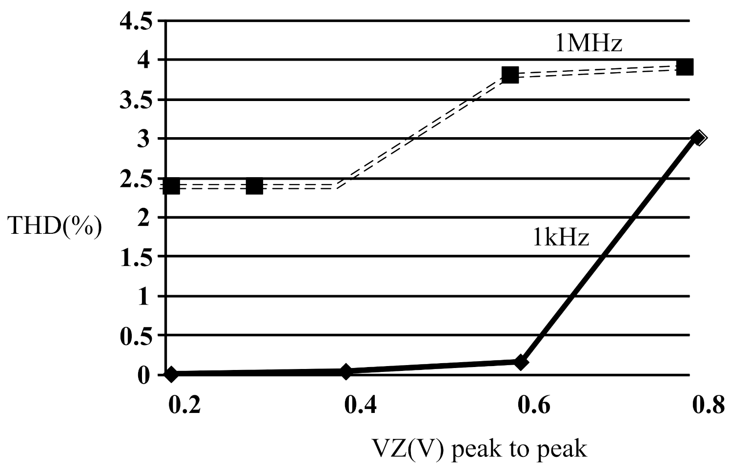
3. Simulation Results
4. Conclusions
Author Contributions
Funding

Conflicts of Interest
References
- Sedra, A.; Smith, K. A Second-Generation Current Conveyor and Its Applications. IEEE Trans. Circuit Theory 1970, 17, 132–134. [Google Scholar] [CrossRef]
- Yesil, A.; Kaçar, F. New Dxccii-Based Grounded Series Inductance Simulator Topologies. Istanb. Univ. -J. Electr. Electron. Eng. 2015, 14, 1785–1789. [Google Scholar]
- Yuce, E.; Cicekoglu, O. The Effects of Non-Idealities and Current Limitations on the Simulated Inductances Employing Current Conveyors. Analog. Integr Circ Sig Process. 2006, 46, 103–110. [Google Scholar] [CrossRef]
- Chang, C.-M. Multifunction Biquadratic Filters Using Current Conveyors. IEEE Trans. Circuits Syst. II Analog. Digit. Signal Process. 1997, 44, 956–958. [Google Scholar] [CrossRef]
- Parveen, T.; Rajput, S.S.; Ahmad, M.T. Low Voltage CCII-based High Performance Cascadable Multifunctional Filter. Microelectron. Int. 2006, 23, 28–31. [Google Scholar] [CrossRef]
- Metin, B.; Pal, K. Cascadable Allpass Filter with a Single DO-CCII and a Grounded Capacitor. Analog Integr Circ Sig Process 2009, 61, 259. [Google Scholar] [CrossRef]
- Soliman, A.M. Current-Mode Oscillators Using Single Output Current Conveyors. Microelectron. J. 1998, 29, 907–912. [Google Scholar] [CrossRef]
- Celma, S.; Martinez, P.A.; Carlosena, A. Approach to the Synthesis of Canonic RC-Active Oscillators Using CCII. IEE Proc. Circuits Devices Syst. 1994, 141, 493–497. [Google Scholar] [CrossRef]
- Khan, A.A.; Bimal, S.; Dey, K.K.; Roy, S.S. Novel RC Sinusoidal Oscillator Using Second-Generation Current Conveyor. IEEE Trans. Instrum. Meas. 2005, 54, 2402–2406. [Google Scholar] [CrossRef]
- Wilson, B. Universal Conveyor Instrumentation Amplifier. Electron. Lett. 1989, 25, 470–471. [Google Scholar] [CrossRef]
- Gift, S.J.G. An Enhanced Current-Mode Instrumentation Amplifier. IEEE Trans. Instrum. Meas. 2001, 50, 85–88. [Google Scholar] [CrossRef]
- Koli, K.; Halonen, K.A.I. CMRR Enhancement Techniques for Current-Mode Instrumentation Amplifiers. IEEE Trans. Circuits Syst. I: Fundam. Theory Appl. 2000, 47, 622–632. [Google Scholar] [CrossRef]
- Čajka, J.; Vrba, K. The Voltage Conveyor May Have in Fact Found Its Way into Circuit Theory. AEU Int. J. Electron. Commun. 2004, 58, 244–248. [Google Scholar] [CrossRef]
- Filanovsky, I.M. Current Conveyor, Voltage Conveyor, Gyrator. In Proceedings of the 44th IEEE 2001 Midwest Symposium on Circuits and Systems; MWSCAS 2001 (Cat. No.01CH37257), Dayton, OH, USA, 14–17August 2001; Volume 1, pp. 314–317. [Google Scholar]
- Koton, J.; Herencsár, N.; Vrba, K. KHN-Equivalent Voltage-Mode Filters Using Universal Voltage Conveyors. AEUE-Int. J. Electron. Commun. 2011, 2, 154–160. [Google Scholar] [CrossRef]
- Safari, L.; Barile, G.; Stornelli, V.; Ferri, G. An Overview on the Second Generation Voltage Conveyor: Features, Design and Applications. IEEE Trans. Circuits Syst. II Express Briefs 2019, 66, 547–551. [Google Scholar] [CrossRef]
- Safari, L.; Barile, G.; Ferri, G.; Stornelli, V. Traditional Op-Amp and New VCII: A Comparison on Analog Circuits Applications. AEU Int. J. Electron. Commun. 2019, 110, 152845. [Google Scholar] [CrossRef]
- Safari, L.; Barile, G.; Stornelli, V.; Ferri, G.; Leoni, A. New Current Mode Wheatstone Bridge Topologies with Intrinsic Linearity. In Proceedings of the 2018 14th Conference on Ph.D. Research in Microelectronics and Electronics (PRIME), Prague, Czech Republic, 2–5 July 2018; pp. 9–12. [Google Scholar]
- Safari, L.; Barile, G.; Ferri, G.; Stornelli, V. High Performance Voltage Output Filter Realizations Using Second Generation Voltage Conveyor. Int. J. RF Microw. Comput. Aided Eng. 2018, 28, e21534. [Google Scholar] [CrossRef]
- Stornelli, V.; Barile, G.; Leoni, A. A Novel General Purpose Combined DFVF/VCII Based Biomedical Amplifier. Electronics 2020, 9, 331. [Google Scholar] [CrossRef] [Green Version]
- Stornelli, V.; Safari, L.; Barile, G.; Ferri, G. A New Extremely Low Power Temperature Insensitive Electronically Tunable VCII-Based Grounded Capacitance Multiplier. IEEE Trans. Circuits Syst. II Express Briefs 2021, 68, 72–76. [Google Scholar] [CrossRef]
- A Second-generation Voltage Conveyor (VCII)–Based Simulated Grounded Inductor-Safari-2020-International Journal of Circuit Theory and Applications-Wiley Online Library. Available online: https://onlinelibrary.wiley.com/doi/abs/10.1002/cta.2770 (accessed on 7 August 2021).
- Safari, L.; Barile, G.; Stornelli, V.; Ferri, G. A New Versatile Full Wave Rectifier Using Voltage Conveyors. AEU Int. J. Electron. Commun. 2020, 122, 153267. [Google Scholar] [CrossRef]
- Barile, G.; Safari, L.; Ferri, G.; Stornelli, V. A VCII-Based Stray Insensitive Analog Interface for Differential Capacitance Sensors. Sensors 2019, 19, 3545. [Google Scholar] [CrossRef] [PubMed] [Green Version]
- Barile, G.; Ferri, G.; Safari, L.; Stornelli, V. A New High Drive Class-AB FVF-Based Second Generation Voltage Conveyor. IEEE Trans. Circuits Syst. II Express Briefs 2020, 67, 405–409. [Google Scholar] [CrossRef]
- Barile, G.; Stornelli, V.; Ferri, G.; Safari, L.; D’Amico, E. A New Rail-to-Rail Second Generation Voltage Conveyor. Electronics 2019, 8, 1292. [Google Scholar] [CrossRef] [Green Version]
- Yesil, A.; Minaei, S. New Simple Transistor Realizations of Second-Generation Voltage Conveyor. Int. J. Circuit Theory Appl. 2020, 48, 2023–2038. [Google Scholar] [CrossRef]
- Palmisano, G.; Palumbo, G.; Pennisi, S. High-Drive CMOS Current Amplifier. IEEE J. Solid-State Circuits 1998, 33, 228–236. [Google Scholar] [CrossRef]
- Safari, L.; Azhari, S.J. A Novel Low Voltage Very Low Power CMOS Class AB Current Output Stage with Ultra High Output Current Drive Capability. Microelectron. J. 2012, 43, 34–42. [Google Scholar] [CrossRef]
- Kumngern, M.; Torteanchai, U.; Khateb, F. CMOS Class AB Second Generation Voltage Conveyor. In Proceedings of the 2019 IEEE International Circuits and Systems Symposium (ICSyS), Sapporo, Japan, 18–19 September 2019; pp. 1–4. [Google Scholar]
- Safari, L.; Minaei, S. A Low-Voltage Low-Power Resistor-Based Current Mirror and Its Applications. J. Circuit. Syst. Comp. 2017, 26, 1750180. [Google Scholar] [CrossRef]
- Available online: https://www.tsmc.com/english/dedicatedFoundry/technology/logic/l_018micron (accessed on 7 August 2021).


| Transistor | W (µm)/L (µm) | Transistor | W (µm)/L (µm) |
|---|---|---|---|
| M1, M2 | 36/0.36 | ML1, ML2 | 0.9/0.45 |
| M3–M4 | 72/0.36 | MC1 | 18/0.9 |
| M5 | 72/0.9 | MC2 | 0.81/0.9 |
| M6 | 792/0.9 | MC3 | 0.9/0.9 |
| M7 | 36/0.45 | MC4 | 9/0.9 |
| M8 | 396/0.45 | M13-M14 | 4.5/0.9 |
| M9 | 720/0.9 | M15, M17 | 0.18/0.36 |
| M10 | 360/0.45 | M16, M18 | 36/0.36 |
| M11–M12 | 3.6/0.18 |
| Transistor | Parameter | Calculated | Simulation |
|---|---|---|---|
| MIB2 | gm | 208 µA/V | 161 µA/V |
| ro | 740 kΩ | 641 kΩ | |
| Vsat | 0.096 V | 0.08 V | |
| MIB5 | gm | 129 µA/V | 107 µA/V |
| ro | 1.25 MΩ | 1 MΩ | |
| Vsat | 0.154 V | 0.159 V | |
| MC1 | gm | 181 µA/V | 130 µA/V |
| ro | 1.2 MΩ | 1.25 MΩ | |
| Vsat | 0.1 V | 0.109 V | |
| MC3 | gm | 207 µA/V | 182 µA/V |
| ro | 740 kΩ | 641 kΩ | |
| Vsat | 0.096 V | 0.09 V | |
| M2 | gm | 48 µA/V | 72 µA/V |
| ro | 1.7 MΩ | 1.02 MΩ | |
| Vsat | 0.012 V | 0.04 V | |
| M4 | gm | 38.4 µA/V | 35 µA/V |
| ro | 3 MΩ | 4.3 MΩ | |
| Vsat | 0.014 V | 0.04 V | |
| M8 | gm | 0.506 µA/V | 0.659 µA/V |
| ro | 298 kΩ | 175 kΩ | |
| Vsat | 0.022 V | 0.04 V | |
| M6 | gm | 0.500 µA/V | 0.571 µA/V |
| ro | 235 kΩ | 390 kΩ | |
| Vsat | 0.037 V | 0.05 V | |
| M12 | gm | 16.6 µA/V | 11.8 µA/V |
| ro | 9.2 MΩ | 8.8 MΩ | |
| Vsat | 0.033 V | 0.047 V | |
| M14 | gm | 13.3 µA/V | 9.7 µA/V |
| ro | 18.8 MΩ | 19 MΩ | |
| Vsat | 0.047 V | 0.06 V |
| Parameter | Calculated | Simulated |
|---|---|---|
| rZ (Equation (18)) | 167 Ω | 217 Ω |
| rY (Equation (7)) | 1.15 kΩ | 973 Ω |
| rX (Equation (8)) | 158 kΩ | 120 kΩ |
| Parameter | Maximum | Minimum | Mean |
|---|---|---|---|
| rY(Ω) | 2.35k | 233 | 745 |
| rX(kΩ) | 395 | 40 | 123 |
| rZ(Ω) | 347 | 143 | 224.3 |
| β | 1.47 | 0.651 | 1.02 |
| α | 0.938 | 0.920 | 0.930 |
| Ix THD at 10 mA and 1 MHz(%) | 3.27 | 1.43 | 2.46 |
| Vz THD at 0.8 V p-to-p and 1 MHz(%) | 8 | 2 | 3.53 |
| Parameter | P | V (Vdd-Vss) | T (°C) | ||||||
|---|---|---|---|---|---|---|---|---|---|
| FF | SF | FS | SS | ±0.99 V | ±0.81 V | −20 | 25 | 80 | |
| rY(Ω) | 956 | 965 | 964 | 972 | 894 | 1 k | 804 | 959 | 1100 |
| rX(kΩ) | 113.7 | 113.8 | 114 | 113.88 | 98 | 129.4 | 93.2 | 113 | 147 |
| rZ(Ω) | 205 | 212 | 213 | 217 | 195 | 233 | 182.8 | 211.4 | 248.1 |
| β | 0.993 | 0.990 | 0.993 | 0.992 | 0.992 | 0.993 | 0.9924 | 0.9971 | 0.9927 |
| α | 0.933 | 0.952 | 0.932 | 0.931 | 0.935 | 0.928 | 0.934 | 0.932 | 0.929 |
| THD at Iin = 1 mA and 1 MHz (%) | 2.44 | 2.31 | 2.24 | 2.36 | 2.37 | 2.3 | 2.36 | 2.43 | 2.48 |
| THD at Vx = 0.8 V p-p and 1MHz (%) | 3.04 | 2.46 | 2.4 | 3.4 | 1.59 | 7.6 | 3.52 | 3.37 | 4.2 |
| Proposed | [16] | [18] | [21] | [25] | [26] | [27] | [29] | |
|---|---|---|---|---|---|---|---|---|
| Class | AB | A | A | A | A | AB | A | AB |
| α(DC, f) - 3dB | (0.953, 50 MHz) | (0.997, 217 MHz) | (0.995, 340 MHz) | (1.017, 330 kHz) | (0.992, 220 MHz) | (0.972, 55 MHz) | (0.968, 2.57 GHz) *(1, 1.92 GHz) ** | (1, 100 GHz) |
| β(DC, f) - 3dB | (0.993, 11 MHz) | (0.998, 200 MHz) | (0.996, 14.6 MHz) | (1.035–108 dB 26 kHz–37 kHz) | (0.978, 22.4 MHz) | (0.996, 165 MHz) | (0.988, 794 MHz) | (0.987, 169.7 MHz) |
| Max IX | 10 mA | 17 μA | 40 μA | 100 nA | 2 mA | 0.5 mA | 1.065 mA | 1.22 mA |
| THD at IX | 1 2.40% | 2 0.10% | NA | NA | 3 3.36% | 3 1.10% | NA | 4 1% |
| rx | 120 kΩ | 1.2 MΩ | 0.8 MΩ | 22 GΩ | 370 kΩ | 522 kΩ | 74.28 kΩ | 273.8 kΩ |
| rY | 973 Ω | 6.7 Ω | 49 Ω | 27 kΩ | 2 mΩ | 23 Ω | 930 Ω | 1.88 kΩ |
| rZ | 217 Ω | 0.7 Ω | 79 Ω | 27 kΩ | 2 mΩ | 160 Ω | 705 Ω * 35 Ω ** | 1.75 kΩ |
| Vdd-Vss | ±0.9 V | ±1.65 V | ±1.65 V | ±0.3 V | ±1.65 V | ±0.9 V | ±0.9 V | ±0.9 V |
| Pd | 0.393 mW | 0.330 mW | 0.7 mW | 96 nW | 0.320 mW | 0.120 mW | 0.622 mW * 0.664 mW ** | 0.179 mW |
| THD at VZ | 5 3.90% | NA | NA | NA | 6 2.48% | 7 2.40% | NA | 8 1% |
| #transistors | 38 | 20 | 16 | 20 | 25 | 37 | 6 * 11 ** | 12 |
| Tech. | 0.18 μm | 0.35 μm | 0.35 μm | 0.18 μm | 0.35 μm | 0.15 μm | 0.18 μm | 0.18 μm |
Publisher’s Note: MDPI stays neutral with regard to jurisdictional claims in published maps and institutional affiliations. |
© 2021 by the authors. Licensee MDPI, Basel, Switzerland. This article is an open access article distributed under the terms and conditions of the Creative Commons Attribution (CC BY) license (https://creativecommons.org/licenses/by/4.0/).
Share and Cite
Safari, L.; Barile, G.; Stornelli, V.; Minaei, S.; Ferri, G. Towards Realization of a Low-Voltage Class-AB VCII with High Current Drive Capability. Electronics 2021, 10, 2303. https://doi.org/10.3390/electronics10182303
Safari L, Barile G, Stornelli V, Minaei S, Ferri G. Towards Realization of a Low-Voltage Class-AB VCII with High Current Drive Capability. Electronics. 2021; 10(18):2303. https://doi.org/10.3390/electronics10182303
Chicago/Turabian StyleSafari, Leila, Gianluca Barile, Vincenzo Stornelli, Shahram Minaei, and Giuseppe Ferri. 2021. "Towards Realization of a Low-Voltage Class-AB VCII with High Current Drive Capability" Electronics 10, no. 18: 2303. https://doi.org/10.3390/electronics10182303
APA StyleSafari, L., Barile, G., Stornelli, V., Minaei, S., & Ferri, G. (2021). Towards Realization of a Low-Voltage Class-AB VCII with High Current Drive Capability. Electronics, 10(18), 2303. https://doi.org/10.3390/electronics10182303