Article

LDPC Decoder Design Using Compensation Scheme of Group Comparison for 5G Communication Systems

1
Biomedical Engineering Research Center, Yuan Ze University, Jungli 32003, Taiwan
2
Department of Electrical Engineering, Yuan Ze University, Jungli 32003, Taiwan
3
Department of Electrical and Electronic Engineering, Universiti Teknologi PETRONAS, Seri Iskandar 32610, Malaysia
*
Author to whom correspondence should be addressed.
Electronics 2021, 10(16), 2010; https://doi.org/10.3390/electronics10162010
Submission received: 8 July 2021 / Revised: 13 August 2021 / Accepted: 17 August 2021 / Published: 19 August 2021

Abstract

:
This paper presents a dual-mode low-density parity-check (LDPC) decoding architecture that has excellent error-correcting capability and a high parallelism design for fifth-generation (5G) new-radio (NR) applications. We adopted a high parallelism design using a layered decoding schedule to meet the high throughput requirement of 5G NR systems. Although the increase in parallelism can efficiently enhance the throughput, the hardware implementation required to support high parallelism is a significant hardware burden. To efficiently reduce the hardware burden, we used a grouping search rather than a sorter, which was used in the minimum finder with decoding performance loss. Additionally, we proposed a compensation scheme to improve the decoding performance loss by revising the probabilistic second minimum of a grouping search. The post-layout implementation of the proposed dual-mode LDPC decoder is based on the Taiwan Semiconductor Manufacturing Company (TSMC) 40 nm complementary metal-oxide-semiconductor (CMOS) technology, using a compensation scheme of grouping comparison for 5G communication systems with a working frequency of 294.1 MHz. The decoding throughput achieved was at least 10.86 Gb/s without evaluating early termination, and the decoding power consumption was 313.3 mW.

1. Introduction

The market for fifth-generation (5G) communication systems is rapidly growing. 5G technology requires low-power and low-cost hardware equipment support because it considers the application requirements of enhanced mobile broadband (eMBB) and massive machine-type communication (mMTC). Immediate applications, such as in telemedicine and autonomous driving, will require ultra-reliable and low-latency communication (URLLC) support. Additionally, the corresponding specifications of the polar code and low-density parity-check (LDPC) code were proposed in the 15th edition of the 5G specification [1] published in 2018.
The error correction capability is of great importance when considering the advances in these techniques. The LDPC code [2], which comprises a forced error-correcting capability and fully parallel decoding architecture, was proposed by Gallager in 1962. Currently, LDPC codes have been introduced in different communication standards, such as DVB-S2 [3], IEEE 802.11n [4], IEEE 802.16e [5], and 5G new-radio (NR).
LDPC is valued by researchers because it has powerful error-correction capabilities that are extremely close to the Shannon limit. However, LDPC has been difficult to implement in previous generations due to the complex calculations. Subsequently, process technology has evolved, and LDPC has been discussed and recently applied to most of the popular 5G communication fields. The requirement to achieve a throughput of 10 Gb/s for the 5G NR standard will also be a significant challenge for LDPC implementation.
With the evolution of technology production, LDPC has been widely used in various communication fields, such as IEEE802.16e, IEEE802.11n, and the NAND flash channels [6]. Today, many approximations exist for the sum-product algorithm originally used in the LDPC, such as simplified versions of the normalized min-sum algorithm (NMSA) [7], the offset min-sum algorithm (OMSA) [8], and the normalized probabilistic min-sum algorithm (NPMSA) [9]. These studies simplify the hardware area, reduce the complexity of routing, and speed up the overall operation speed. Despite these advantages, they are inevitably accompanied by a loss in the error correction capability. In this study, we propose a flexible compensation scheme based on the NPMSA to achieve hardware simplification and recovery error correction ability. Without derivation, the proposed method was roughly verified in [10] for the LDPC decoding under the NAND flash channels. The contributions of this paper are that we explore the proposed compensation scheme using a thorough algorithm derivation with simulations, a detailed architecture design, a prototyping chip verification, and comparisons among several LDPC decoder chips. Simulation results reveal that the proposed compensation scheme operates effectively in different applications. Regarding the hardware implementation of the LDPC decoder for 5G communication systems, we adopted layered decoding, which is suitable for high-parallelism operations to achieve high throughput. For reference, the study in [11] proposed a further effective means of improving decoding performance of an LDPC code by extending single-decoder decoding to parallel decoding with multiple sub-decoders.
The remaining sections are organized as follows. In Section 2, the decoders for the LDPC and QC-LDPC codes are introduced. In Section 3, the fundamentals of decoding and algorithms are described. We determine the NPMSA used in the successive sections. In Section 4, we describe the characteristics of the first and second probabilistic minimum. Based on these characteristics, we introduce the proposed compensation scheme to recover the decoding capability and maintain hardware simplification. In Section 5, we describe the architecture of the LDPC code design for different matrices, using base graph 1 (BG 1) and base graph 2 (BG 2) in the 5G NR standard. The post-layout results and a comparison of this study with related studies is subsequently presented. Finally, Section 6 provides a conclusion to this paper.

2. Low-Density Parity-Check Codes

LDPC is a type of simultaneous equation that consists of a sparse matrix H. Each row of the H matrix represents a check node (CN) and each column represents a variable node (VN). The 1s elements in the H matrix are dependent on the CNs and VNs. The 0s elements in the H matrix are ignored. The data transmission relationship between the CNs and VNs can be expressed using the Tanner graph [12].

2.1. Quasi-Cyclic (QC) LDPC Codes

Quasi-cyclic (QC) LDPC codes [13] are more efficient in the hardware implementations of LDPC codes. In the (N, M) QC-LDPC H matrix, N represents the number of base columns, and M represents the number of base rows. The maximum number of VNs connected to a row is defined as w r (row weight), and the maximum number of CNs connected to a column is defined as w c (column weight). Each element of the H matrix can be treated as an identity matrix, which can be expanded to provide a z × z sub-matrix with a right shift. Therefore, the H matrix is a simplified version of the (N, M) QC-LDPC. The code rate (R) is the proportion of real information (NM) in the transmission data (N), and is regarded as R = N M N . Each element in the H matrix represents the number of right shifts. In the H matrix, all elements in a single layer are independent, enabling the operations in a single layer to run synchronously. The maximum parallelism of the hardware design can be up to a maximum value of z. This efficiently speeds up the overall operations and improves the overall throughput. The QC-LDPC is composed of a cyclic-shifted identity matrix; thus, a memory address can be obtained using the cyclic-shifted characteristic. Only the starting point of the memory address is required to make the design of the reading memory address more flexible.

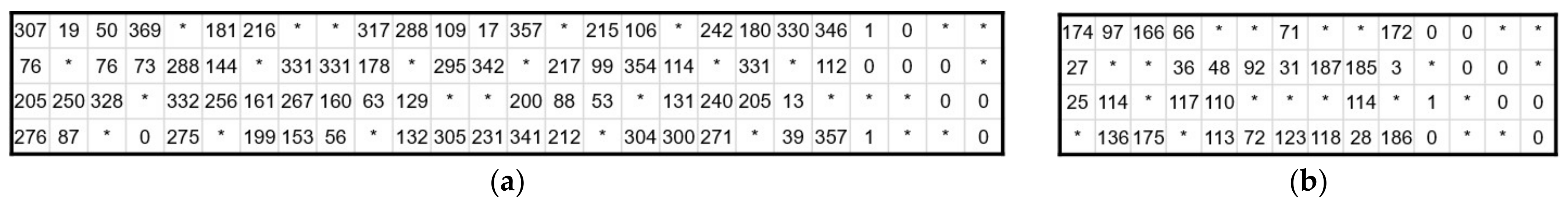
2.2. Parity Check Matrices for 5G NR Standard

The H matrix of the LDPC code in the 5G NR specification conforms to the QC-LDPC code, so we designed the dual-mode LDPC decoder according to the characteristics of the QC-LDPC code. The 5G NR specification is typically divided into BGs 1 and 2. It is subdivided into eight different lifting sizes for each BG. We adopted two different specifications for H, achieved without rate-matching. The first matrix comes from index 1 of the BG1. As shown in Figure 1a, the base matrix is a 4 × 26 QC-LDPC code with a code rate of 11/13, w r = 19 , and w c = 4 . The second matrix comes from index 1 of the BG 2. As shown in Figure 1b, the base matrix is a 4 × 14 QC-LDPC code with a code rate of 5/7, w r = 10 , and w c = 3 . The code lengths were 9984 and 5376 in BG 1 and BG 2, respectively. For the details of the 5G NR QC-LDPC encoder design, readers can refer to [14,15].

3. LDPC Decoding Algorithms

The original LDPC decoding algorithm was the sum-product algorithm (SPA) [16]. The SPA can almost achieve the theoretical decoding ability, but it is difficult to implement because of the excessively complex calculations. Therefore, alternative algorithms have been published, such as the NMSA and OMSA. Both algorithms use approximate values adjusted by a normalized or offset coefficient to simplify the overall operation complexity and maintain the approximate decoding capability of the SPA. It is noteworthy that the NMSA was widely used for a decade in the hardware implementations of LDPC decoders. Furthermore, additional discussions and research on simplifying the hardware complexity of the NMSA have been published, such as the NPMSA, approximate extrinsic minima (rExMin) algorithm [17], second minimum approximation min-sum algorithm (SMA-MSA) [18], and single variable weight min-sum algorithm (svwMSA) [19]. These algorithms are dedicated to alleviating the problems of high hardware complexity and area cost, which are caused by the operations of comparators. Although these studies successfully alleviated the above problems, the decoding capability was weakened. Below, we introduce the details of the algorithms and their differences.

3.1. NMSA

The operation flow of the NMSA using a layered scheme can be divided into four steps. In the NMSA, we initially define y j as the received channel information, C j as the initial prior message, Q i , j k as prior messages, and R i , j k as the extrinsic message, where i is the index of the row of H, j is the index of the column of H, and k is the index of the decoding iteration. Subsequently, the core decoding processes are stated as follows.
In the first step, all parameters in the decoder must be initialized. The received channel information y j is then imported and stored in the memory for subsequent operations. The logarithm expression of the initial prior message C j for each VN is stated as:
C j = l o g P x j = 0 y j P x j = 1 y j .
The prior messages Q i , j 0 are updated as C j , which is the log likelihood ratio (LLR), and the extrinsic messages R i , j 0 are zeros.
In the second step, the prior message Q i , j k is updated by subtracting the R i , j k 1 from the L L R j to recover the decoding capability in the last iteration. The inclusion of the two conditions above in the updates is called a prior message process. The formula for the updated prior message is shown as:
Q i , j k = L L R j R i , j k 1
In the third step, the check nodes R i , j k are updated to find the bits that have the lowest reliability in every layer. The check node process contains the product of the total sign excluding the updated node, the first minimum excluding the updated node, and the scaling factor γ . The set of VNs corresponding to CN is denoted as N c . The formula for updating the check nodes is expressed as:
R i , j k = γ · j N c \ j s g n Q i , j k m i n j N c \ j Q i , j k
In the fourth step, the variable node L L R j is updated with Q i , j k added to an extrinsic message R i , j k to increase the reliability of the correct nodes and correct the bits that have lower reliability and a higher error rate in every layer. The formula for updating the variable nodes is expressed as:
L L R j = Q i , j k + R i , j k
Subsequently, the NMSA iteratively processes the second to fourth steps until k reaches the maximum iterations or the early termination scheme is satisfied.

3.2. NPMSA

Generally, the critical path of the decoder hardware design employing the NMSA is the operation of the check node process. This is because numerous comparator operations cause severe operational delays. Therefore, the NPMSA was proposed to speed up the overall operation and relieve the hardware burden of the NMSA, which includes area and routing costs. The NPMSA adopts a grouping search that divides the prior message Q i , j k into G groups, to replace the sorter used by the NMSA. In each group of the NPMSA, the architecture only needs to be implemented using 2-to-1 comparators [20]. A significant reduction in the architecture overhead is noted when compared to the sorter using 2-to-2 comparators. The gap of the hardware burden between the grouping search and sorter increases as the number of prior messages Q i , j k increases. However, in alleviating the effects of hardware burden, a grouping search cannot accurately determine the correct second minimum. This is because the correct second minimum is typically lost after every 2-to-1 comparator operation in the hardware design. This causes the accuracy of the algorithm to decrease and directly affects the decoding capability. The formula for updating the check nodes with a grouping search is expressed as:
R i , j k = γ · j N c \ j s g n Q i , j k m i n 1 s t , j j i n d e x m i n 2 n d , j = j i n d e x ,
where:
m i n 1 s t = m i n j N c Q i , j k ,
and the probabilistic second minimum is:
m i n 2 n d = m a x min j G L Q i , j k , min j G R Q i , j k .
The index j i n d e x denotes the position of the first minimum. G L and G R represent the left and the right groups of the prior message Q i , j k , respectively, when there are two groups.
Table 1 lists a comparison of the check node process executed using the NMSA, the split-row threshold algorithm (SRTA) [21], and NPMSA. The two-input comparison was used as the basis for comparison. From an algorithmic perspective, the NPMSA can reduce the number of two-input comparisons by 49.1%, with a 0.05 dB loss in the error-rate performance, compared to the NMSA. Compared to the SRTA, the NPMSA can reduce the number of two-input comparisons by 35.4%, with a 0.15 dB enhancement in error-rate performance.
It is noteworthy that the probabilistic second minimum value in Equation (7) is equal to the correct second minimum value in Equation (3) when the correct second minimum value is not in the same group of the correct first minimum value. This means that the correct second minimum value can be easily achieved when the number of groups becomes larger. However, a large number of groups intensifies the hardware burden because of the increment of 2-to-2 comparators. Additionally, the occurrence of differences between the correct and probabilistic second minimum values results in a decline in the decoding capability. The NPMSA suffers from a high error floor region, which was revealed in [18]. Thus, the difference between the correct and probabilistic second minimum values must be reduced when the difference occurs.

3.3. rExMin Algorithm

Based on the NPMSA, the rExMin algorithm was proposed to revise the problem caused by a decline in the decoding capability due to a difference between the second minimum and the probabilistic second minimum. The rExMin algorithm uses a negative factor θ to reduce the value of the probabilistic second minimum, which reduces the difference and recovers the decoding capability. In addition, the negative factor θ may cause overcorrection when the new second minimum is smaller than the first minimum. Therefore, a comparator was added to determine whether overcorrection occurred. The new second minimum is the same as the probabilistic second minimum when overcorrection occurs. The new second minimum is the sum of the probabilistic second minimum and the negative factor θ . The formula for updating the check nodes with a grouping search is expressed as:
n e w   m i n 2 n d = m i n 2 n d , m i n 2 n d + θ < m i n 1 s t m i n 2 n d + θ , m i n 2 n d + θ m i n 1 s t .

3.4. SMA-MSA

The concept of SMA-MSA is the same as that of the rExMin algorithm. The SMA-MSA treats the probabilistic second minimum as the upper bound and the first minimum as the lower bound. Combining the first minimum and probabilistic second minimum, the SMA-MSA obtains the new second minimum, as shown below:
n e w   m i n 2 n d = ρ 2 · m i n 1 s t + σ · m i n 2 n d ,
where both ρ 2 and σ are used to weigh the first minimum and probabilistic second minimum for the new second minimum. The values of ρ 2 and σ are set as 2 x or ( 1 2 x ) , depending on the code, where x is an integer. The author of SMA-MSA noted that the new second minimum auto-adjusted the correction value applied to the first minimum by a factor ρ . The definition of ρ is expressed as:
ρ = ρ 2 + m i n 2 n d m i n 1 s t · σ .
The formula of the check nodes updated with the grouping search is shown below:
R i , j k = j N c \ j s g n Q i , j k ρ · m i n 1 s t , j j i n d e x n e w   m i n 2 n d , j = j i n d e x .

4. Proposed Compensation Scheme for NPMSA

The NPMSA is adopted in a LDPC decoder design to reduce the hardware area cost, to relieve the complexity of routing, and to accelerate the operation of numerous comparators. However, the accuracy of the algorithm is decreased compared to the NMSA. Therefore, the balance between hardware complexity, overall calculation speed, and decoding capability is important. To resolve the algorithm accuracy problem, the rExMin algorithm [17] and the SMA-MSA [18] were proposed as the alternative methods for the NPMSA. Their concepts are based on reducing the gap between the accurate second minimum and the probabilistic second minimum to recover the decoding capability. We continue these concepts and modify the probabilistic second minimum using a flexible adjustment.

4.1. Difference in Extrinsic Messages

The NMSA derived from the simplified SPA leads to larger values due to the simplified process. Larger values cause the accuracy of the algorithm to decrease and directly affect the decoding capability. Therefore, NMSA combines the larger values with the normalized scaling factor γ to reduce the difference in the check node process. Similarly, the NPMSA derived from the simplified NMSA leads to a loss in accuracy of the accurate second minimum due to the adoption of a grouping search. In a grouping search, 2-to-1 comparators are used to search for the first minimum and the probabilistic second minimum. Because the probabilistic second minimum in the NPMSA would be greater than the second minimum in the NMSA, the gap between the first and second minimum in the NPMSA is greater than that gap in the NMSA. This gap in the NPMSA causes the accuracy of the algorithm to decrease and directly affects the decoding capability. Thus, the basic idea of the proposed improved normalized probabilistic min-sum algorithm (INPMSA) [10] is to reduce the gap or close the gap between the first minimum and the second minimum in the NMSA, thus enabling the decoding capability to be recovered. With regard to hardware implementation, the INPMSA maintains its advantages by reducing the area cost and complexity of routing, and accelerates the overall operation speed.

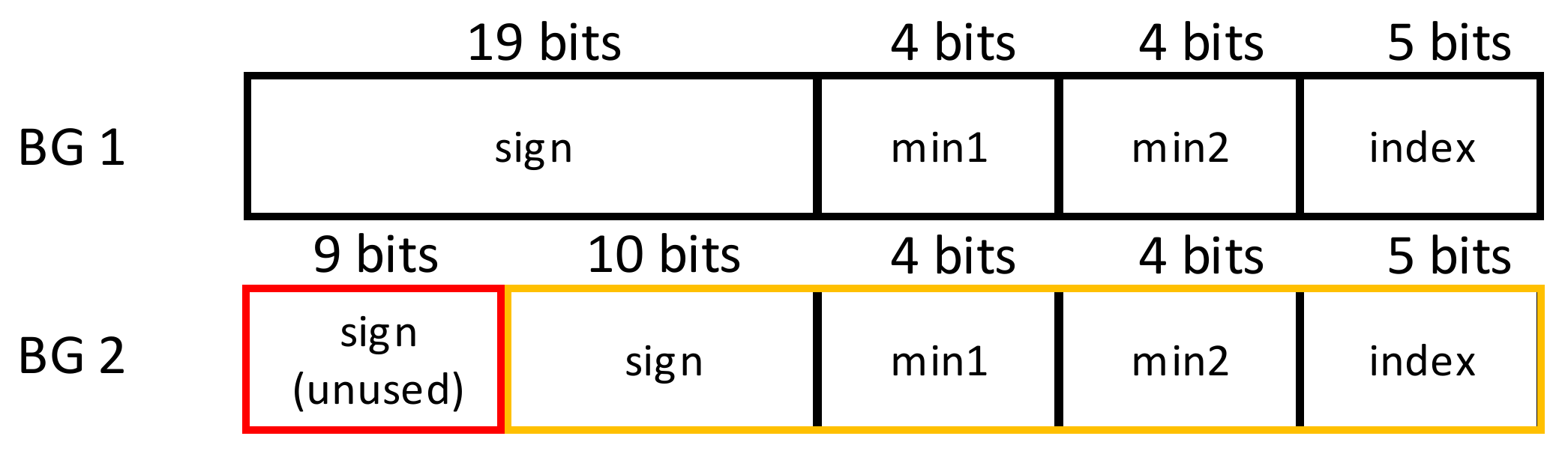
4.2. INPMSA with Compensation Scheme

To reduce the hardware area cost and the complexity of routing, the proposed method adopts a grouping search in check node updating. Additionally, we focus on the gap between the first minimum and the probabilistic second minimum to recover the decoding capability. Because the grouping search can still find the accurate first minimum in check node updating, we used the first minimum as the basis for adjusting the value of the probabilistic second minimum. An increase was noted in the reliability of the check nodes as the number of iterations increased. To deal with the change in reliability, INPMSA adopts proportional adjustment to improve the probabilistic second minimum. Additionally, the first minimum and the improved probabilistic second minimum need to be multiplied by the scaling factor to reduce the difference from the NMSA. We took α and β to represent the proportions of the first minimum and the probabilistic second minimum, respectively. The new second minimum is expressed as:
n e w   m i n 2 n d = α γ m i n 1 s t + β γ m i n 2 n d .
The decoder loses error correction capability when the new second minimum is less than the first minimum, or greater than the probabilistic second minimum. We call this the reversal problem, which results in overcorrection or correction failure. To avoid these problems, we define the upper and lower bounds as the probabilistic second minimum and first minimum, respectively. Initially, we set the scaling factor γ = 1 for Equations (3), (5) and (12) to simplify the following deduction. We then derive the range of α and β using the upper (Case 1) and lower (Case 2) bounds, which are shown below:
Case 1—The new second minimum must be less than or equal to the probabilistic second minimum, as shown below:
n e w   m i n 2 n d m i n 2 n d .
α m i n 1 s t + β m i n 2 n d m i n 2 n d .
β 1 α · m i n 1 s t m i n 2 n d .
Case 2—The new second minimum must be greater than or equal to the first minimum, as shown below:
n e w   m i n 2 n d m i n 1 s t .
α m i n 1 s t + β m i n 2 n d m i n 1 s t .
β 1 α · m i n 1 s t m i n 2 n d .
Combining the two cases above, we observed that the relationship between α and β is related to the ratio of the first minimum and the probabilistic second minima. Then we can have:
1 α · m i n 1 s t m i n 2 n d β 1 α · m i n 1 s t m i n 2 n d .
Because the probabilistic second minimum must be greater than the first minimum, the ratio of the first minimum and the probabilistic second minima must be less than 1. Then we can have:
m i n 1 s t m i n 2 n d 1 .
By combining Equations (19) and (20), we can conclude that this case is only valid when the first minimum is equal to the probabilistic second minimum. Subsequently, we can achieve:
α + β = 1 ,
where α and β must be greater than or equal to 0 to avoid changing the original gap between the first minimum and the probabilistic second minimum.
The number of groups directly affects the error probability of the probabilistic second minimum and the values of α and β . The relationship between the error probability of the probabilistic second minimum and the number of groups is calculated as:
E r r o r   p r o b a b i l i t y = C 2 Q G · G C 2 Q = Q G Q G G ,
where Q denotes the total number of Q i , j k in a layer (i.e., the number of row weights in a layer), and G represents the number of groups. Table 2 lists the calculated error probabilities of the probabilistic second minimum for different groups and inputs. We can observe that the higher the number of groups, the lower the error probability of the probabilistic second minimum. The basic idea of the proposed INPMSA is that an increase in the error probability of the probabilistic second minimum is due to an increase in the proportion of the first minimum used for improvement. For hardware implementation, we defined α as 2 x and β as ( 1 2 x ) , where x is a positive integer. In this case, α is the error probability of the probabilistic second minimum or smaller.

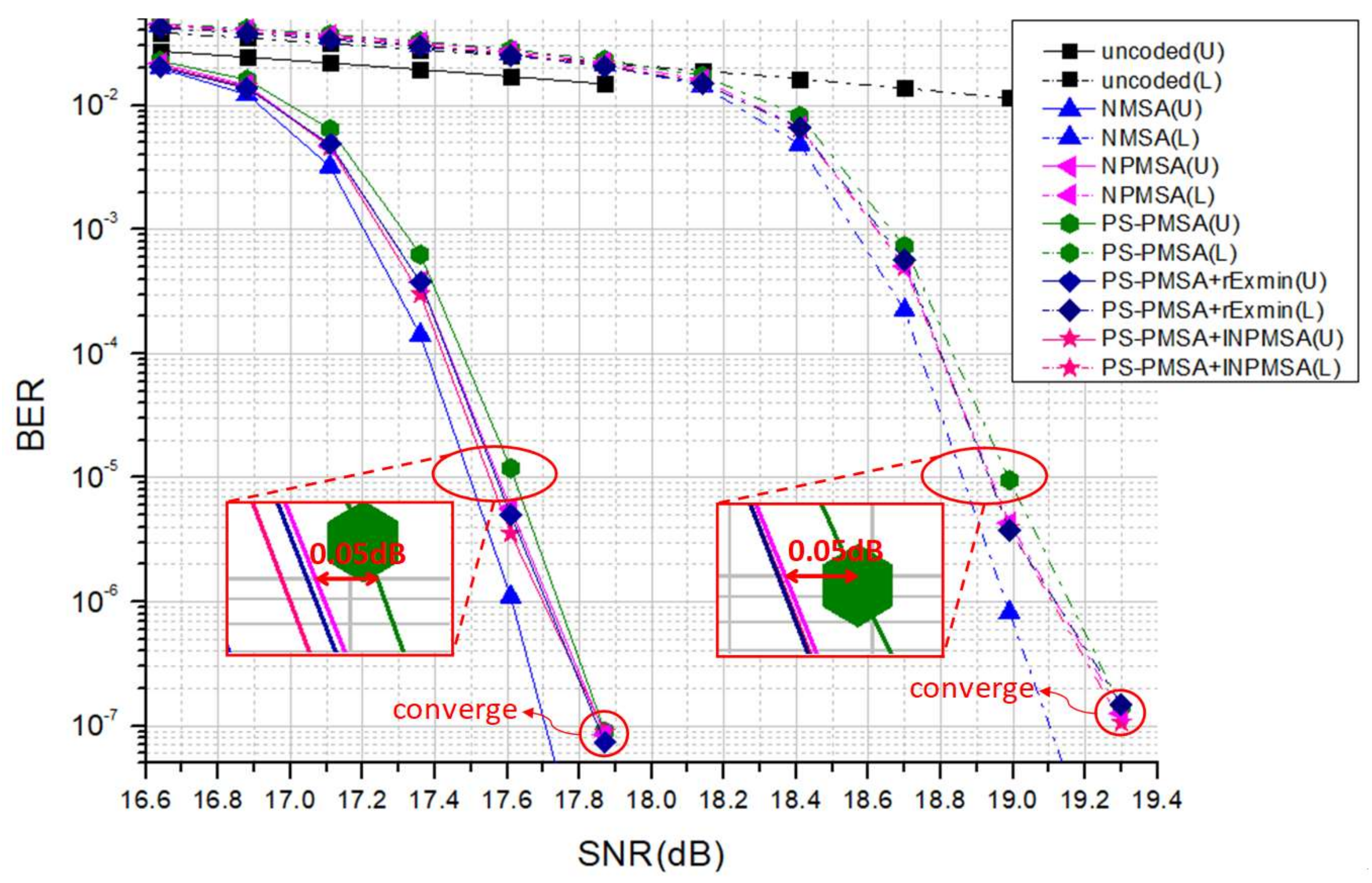
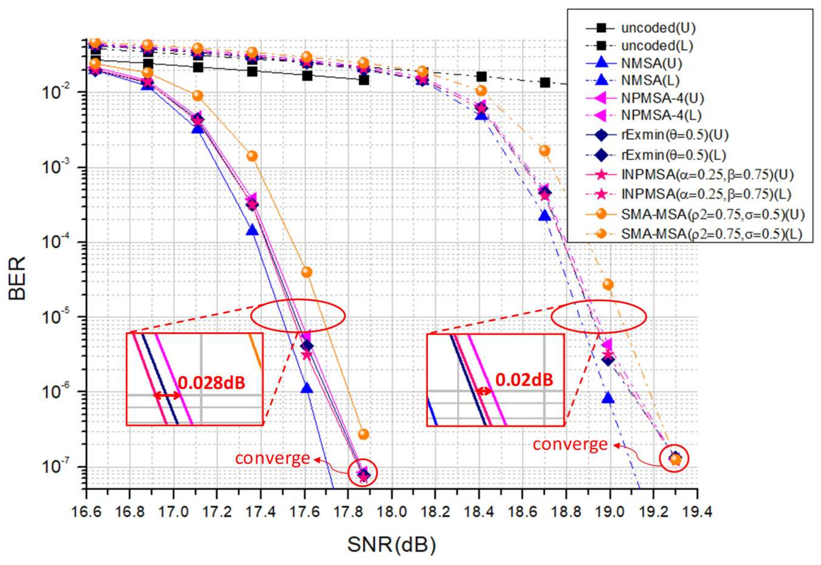
4.3. Simulation Results

The proposed methods implemented the floating-point bit-error rate (BER) performance on NMSA and NPMSA using improved methods based on layer decoding under the rate-5/6 (1944, 324) QC-LDPC code; with early termination and different improving algorithms, row weight w r = 20, scaling factor γ = 0.75, and maximum iteration = 20 for the IEEE 802.11n, as shown in Figure 2. The NPMSA-2 and NPMSA-4 represent NPMSAs with 2 Group and 4 Group searches, respectively. The BER performance of INPMSA-4 with α = 0.5 and β = 0.5 is worse than that of the NPMSA-2. However, the INPMSA-4 with α = 0.125 and β = 0.875 significantly improves the BER performance when α is selected using a smaller value of error probability listed in Table 2. The BER performance between the INPMSA-4 with α = 0.125 and β = 0.875, and the rExMin algorithm using the 4 Group search with θ = 0.5, are approximately the same. There is a similarity in the decoding performance between SNR = 4.0 dB and SNR = 4.5 dB, showing that the INPMSA-4 with α = 0.125 and β = 0.875 can achieve better decoding performance than the NPMSA-4, without improvement in the SNR. In comparison to the SMA-MSA, the INPMSA-4 can achieve a coding gain of about 0.15 dB when the BER = 10−5. This is because the SMA-MSA does not consider the reversal problem, which causes the degradation of the decoding performance due to the use of the inappropriate new second minimum.
In the NAND flash channel model, the BER performance is based on the rate-0.89 (9728, 1024) LDPC code, which uses early termination and different improvement algorithms, a scaling factor γ = 0.75, row weight w r = 36, and maximum iteration = 8. The dashed lines in Figure 3 denote the results of the lower page. The solid lines denote the results of the upper page. The proposed decoder [9] suggests that dividing Q i , j k into four groups can achieve the best decoding performance and hardware implementation. Therefore, we adopted four groups of minima finders. There is a reversal problem in the performance of the SMA-MSA, which caused the decoding performance to decline. The performance of the INPMSA is similar to that of the rExMin algorithm when Q i , j k is divided into four groups. Compared to the NPMSA, the INPMSA can reach approximately 0.028 and 0.02 dB in the upper and lower pages, respectively, when the BER = 10−5. When the BER performance drops below 10−6, the decoding capability starts to converge, with the exception of the NMSA. From the above simulation results, the INPMSA is capable of avoiding the reversal problem and efficiently achieves the correction effect to improve the decoding capability.
In addition, we applied the INPMSA to models implemented in related studies using the NPMSA to observe the practicability of the NAND flash channel model. We referred to the partially stopped probabilistic min-sum algorithm (PS-PMSA) [22], which discards the unnecessary operations in check node updating using error-correcting degradation, as shown in Figure 4. Comparing the NPMSA and the PS-PMSA shows a 0.05 dB coding gain when the BER = 10−5. After combining the PS-PMSA with the INPMSA, the improved PS-PMSA can further achieve decoding capabilities consistent with the NPMSA, and still discard the unnecessary operations in check node updating.
For the design of the hardware to the 5G NR standard, we simulated and analyzed the decoding performance using the 5G NR BGs 1 and 2. In BG 1, the analysis of the BER performance was based on the rate-11/13 (9984, 1536) LDPC codes that have early termination and different improving algorithms, a scaling factor γ = 0.75, row weight w r = 19, and maximum iteration = 6. Figure 5a shows that the performance between the NPMSA-2 and NPMSA-4 has a 0.38 dB coding gain when the BER = 10−6. Figure 5a also shows that the INPMSA-2 significantly improves the BER performance when α is selected using a smaller value of error probability listed in Table 2. However, the BER performance of INPMSA-4 with α = 0.5 and β = 0.5 is worse than that of the NPMSA-4. The coding gain of the INPMSA-4 with α = 0.25 and β = 0.75 can be achieved. Figure 5a indicates that the decoding capability of the NPMSA starts to converge after a SNR = 4.5 dB, and this characteristic ensures the decoding capability of the INPMSA with α = 0.25 and β = 0.75, SMA-MSA, and the rExMin algorithm, is the same.
In BG 2, the BER performance was based on the rate-5/7 (5376, 1536) LDPC codes, which have early termination and different improving algorithms, a scaling factor γ = 0.75, a row weight w r = 10, and a maximum iteration = 6. Figure 5b shows that the performance between the NPMSA-2 and NPMSA-4 has a 0.4 dB coding gain when the BER = 10−5. Figure 5b also shows that the INPMSA-2 significantly improves the BER performance. The BER performance of the INPMSA-4 with α = 0.5 and β = 0.5 is worse than that of the NPMSA-2. However, the INPMSA-4 with α = 0.25 and β = 0.75 improves the BER performance when α is selected using a smaller value of error probability listed in Table 2. The coding gain between the best performance of the INPMSA-2 and INPMSA-4 is 0.25 dB when the BER = 10−6. Figure 5b also indicates that the decoding capability of the INPMSA-4 with α = 0.25 and β = 0.75, SMA-MSA, and the rExMin algorithm starts to converge after the SNR = 4.5 dB.

5. VLSI Implementation of Dual-Mode LDPC Decoder for 5G NR Systems

The proposed dual-mode LDPC decoder is designed to support two different 5G NR matrices with the same extension factor of 384. To support two completely different matrix designs, we adopted two controllers to manage the data flow and achieve shared memory. In the calculation unit, multiplexers are used to support different matrix operations. The details of the VLSI implementation are introduced in this section. The proposed LDPC decoder uses a 4 × 26 base matrix in BG 1 index 1, with a code rate = 11/13, and w r = 19. The 4 × 14 base matrix in BG 2 index 1 has a code rate = 5/7 and w r = 10. Both are QC-LDPC codes and the expending factor is equal to 384.
The total bits that contain one sign bit, integer bits, and fraction bits for the posterior and extrinsic messages of the proposed decoder are extracted from fixed-point simulations for the 5G NR BGs 1 and 2. First, we use six to nine bits for the posterior and extrinsic messages in 5G NR BG 1. The simulation shows that eight bits are sufficient for BG 1. In BG 2, the simulation shows that seven or eight bits are sufficient. Thus, we decided to use eight total bits for both the posterior and extrinsic messages. According to Equations (3) and (4), the posterior message is summed by an extrinsic message and a prior message. Hence, we can reduce the unnecessary integer bits of the extrinsic message to relieve the hardware burden based on the integer bits of the posterior message. In addition, we can add fraction bits of extrinsic messages to enhance the accuracy and improve the decoding capability. Four to seven integer bits, and one fraction bit of extrinsic messages, can be performed very close to the floating-point simulation when the SNR = 4.5 dB. Eventually, we chose eight total bits for posterior messages and five total bits for extrinsic messages.

5.1. Architecture of Dual-Mode LDPC Decoder

The proposed overall decoding architecture with layered decoding is shown in Figure 6. This architecture is composed of an input buffer, an output buffer, a posterior message memory, an extrinsic message memory, a network, a de-network, an early termination, and 64 arithmetic units (AUs). The AU contains a prior message unit (PMU), a check node unit (CNU), a variable node unit (VNU), and first in first out (FIFO) buffer. The posterior message memory and extrinsic message memory are composed of a two-port register-based memory. For the posterior message memory, the quantization of posterior messages is eight bits (one sign bit plus seven total bits) and the maximum number of posterior messages is 384 × 26 = 9984 . Hence, the total number of bits of the posterior message memory is 8 × 9984 = 79,872 . Because the decoder only reads 64 consecutive posterior messages from a single block at a time, we divided the posterior message memory into 26 memory blocks and 64 memory banks for each memory block. For the extrinsic message memory, the quantization of the extrinsic message is five bits. To reduce the bandwidth of the extrinsic message memory, the extrinsic messages are stored as individual signs in a layer: m i n 1 s t , m i n 2 n d , and i n d e x m i n . As shown in Figure 7, we divided individual signs into nine bits and ten bits because w r = 19   and   10 in BGs 1 and 2, respectively. The m i n 1 s t , m i n 2 n d , and absolute value of the extrinsic message are scaled so the data length is 4 bits. According to the maximum w r = 19 , the i n d e x m i n is stored as five bits. The maximum number of layers is 4 × 384 = 1536 , but there are 32 bits to store extrinsic messages for each layer, so the total number of bits of the extrinsic message memory is 32 × 1536 = 49,152 . Because the parallelism is 64, we combine 64 consecutive extrinsic messages into a string. Because the base columns and w r in BG 2 are smaller than those in BG 1, some posterior and extrinsic memories are unused. Hence, the gated clock technique is adopted to reduce the power of the unused memory.

5.2. CNU Using Compensation Scheme of Group Comparison

Figure 8a illustrates the architecture of the CNU and Figure 8b illustrates the architecture of the min and index finder, and the scaler, in the proposed INPMSA. First, the prior message is stored in the D-flip-flop for the pipeline after receiving prior messages from the PMU. The prior message is then transmitted to a sign bit and absolute value. The individual sign bit for each row weight is then generated by the “XOR sign” module after which the I n d e x m i n , m i n 1 s t , and m i n 2 n d are generated by the Min & Index Finder. In the scaler, the m i n 1 s t and m i n 2 n d are multiplied by the scaling factor ( γ = 0.75) and improved factor ( γ α = γ β = 0.375), respectively. Finally, this data is combined with an extrinsic message and transferred to the VNU. Additionally, Table 2 listed in [10] reveals that the scaler in the INPMSA is simpler and faster than that in the rExMin by approximately one comparator. It demonstrated that the hardware implementation result of the CNU used 36 inputs and divided them into four groups: the NPMSA, the INPMSA, and the rExMin algorithm. The INPMSA has a critical path that is increased by approximately 0.3 ns due to the addition of a compensation scheme. Compared to the rExMin, the INPMSA is approximately 0.08 ns faster. By comparing the comprehensive decoding ability and hardware operation speed, we found that the INPMSA can maintain the same decoding capability as the rExMin, and has more advantages during hardware implementation.

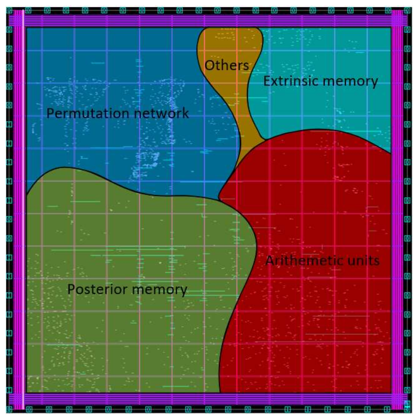
5.3. Post-Layout Implementation Results

Using the ASIC design flow, the decoder is synthesized and implemented using the Taiwan Semiconductor Manufacturing Company (TSMC) 40 nm complementary metal-oxide-semiconductor (CMOS) process with a working frequency of 294.1 MHz. There are three major costs located in the posterior and extrinsic memory, with a cell area of approximately 42.2%; arithmetic units with 64 parallelisms and a cell area of about 25.2%; and the network/de-network in pipelines with a cell area of approximately 22.7%. The proposed dual-mode LDPC decoder operates with two different code lengths, and the highest throughput meets the throughput requirement of the 5G NR standard, which is higher than 10 Gb/s. To evaluate the throughput of the proposed dual-mode LDPC decoder, the throughput estimation equations used for the decoder are as follows:
T h r o u g h p u t   T P = C L × f z P + N p i p e × N r o w × N i t e r ,
where C L and f denote the code length and frequency, respectively; z and P are the expending factor and number of parallelisms, respectively; and N p i p e , N r o w , and N i t e r represent the number of pipeline stages, the base row, and the maximum iterations, respectively. Without employing the early termination, the throughput reaches at least 10.86 and 5.84 Gb/s in BG 1 and BG 2, respectively. The highest throughput of the decoder in BG 1 mode can exceed the throughput requirement of 10 Gb/s for the 5G NR systems.
Figure 9 illustrates the chip layout and Table 3 lists the summary of post-layout results of the proposed dual-mode LDPC decoder. Table 3 also lists a comparison of recent studies for the 5G NR systems. The studies in [23,24] achieved post-layout and post-synthesis (pre-layout) implementations, respectively. Compared to the post-synthesis implementation, the post-layout implementation contains more hardware information, including the logic gate placements, clock tree synthesis, and wire routing. It is worth noting that the studies in [23,24] focused on the low code-rate (high correcting ability) LDPC decoding and this study focused on the high code-rate (high transmission rate) LDPC decoding for the 5G NR systems. Thus, it is hard to compare these application-specific integrated circuits (ASICs) because their design parameters are very district. To achieve a fair evaluation of the LDPC decoder ASICs using the distinct CMOS processes, however, the normalized area efficiency (NAE) and energy efficiency (NEE) are widely used [25] and evaluated in terms of the 40 nm CMOS process in this study. The NAE denotes how many decoded bits per unit area can be achieved in the decoder. The NEE denotes how much energy per decoded bit is consumed in the decoder. In early 2021, the study in [23] proposed the LDPC decoder ASIC for the 5G NR standard using a layered combination min-sun algorithm (CMSA) decoding to achieve the features of low complexity and high throughput. It supports a low rate-1/3 BG 1 with a code length of 3808. Using the TSMC 65 nm CMOS process, it achieves a maximum throughput of 3.04 Gb/s with a NAE of 7.18 bits/mm2 and a NEE of 42.48 pJ/bit. To further support the low rate-1/3 BG 1 with the maximum code length of 25,344 and low rate-1/2 BG 2 with a maximum code length of 19,200 in the 5G NR standard, the study in [24] proposed a reconfigurable LDPC decoder ASIC using a layered NMSA decoding accompanied with instruction-level reordering and data-level rescheduling. Because it achieves 33.2 Gb/s/iteration using the TSMC 28 nm CMOS process, the throughput rates are 6.64 Gb/s at average iterations of 5, and 7.92 Gb/s at average iterations of 4.92, for the rate-1/3 BG 1 and rate-1/2 BG2 LDPC decoding, respectively. Compared to [23,24], the proposed dual-mode decoder using the layered INPMSA decoding achieves a high throughput of 10.86 Gb/s, which meets the requirement of 5G NR application with a high NAE of 11.40 bits/mm2 and low NEE of 28.85 pJ/bit. This reveals that the INPMSA using the proposed compensation scheme achieves a low silicon area with low energy consumption.

6. Conclusions

In this paper, we proposed a dual-mode LDPC decoder for 5G NR systems. This design can support the rate-11/13 BG 1 and rate-5/7 BG 2 matrices. We adopted the layered decoding schedule with 64 parallelisms for hardware implementation to reach the throughput requirement of the 5G standard. Additionally, the sorter in the CNU was replaced by a grouping search to reduce the critical burden of the CNU. This saves half of the comparator demand at the same calculation speed, with a decline in the decoding capability. To alleviate the decline in the decoding capability, we proposed a compensation scheme to revise the probabilistic second minimum using the first minimum and proportion fixing. Compared to the SMA-MSA, the proposed compensation scheme is more complete and exhibits a better decoding performance. The proposed INPMSA also achieves the same decoding capability as the rExMin algorithm and accelerates operations at the comparator stage. Finally, the post-layout implementation of the proposed dual-mode LDPC decoder was achieved using the TSMC 40 nm CMOS process at an operating frequency of 294.1 MHz, a core area of 3.24 mm2, and power consumption of 313.3 mW. The decoding throughput can reach at least 10.86 and 5.84 Gb/s when the mode is BG 1 and BG 2, respectively. The throughput does not consider early termination, so the higher throughput can be achieved at a higher SNR.

Author Contributions

Conceptualization, C.-H.L. and C.-X.W.; methodology, C.-H.L. and C.-X.W.; software, C.-X.W.; validation, C.-H.L., C.-X.W. and C.-K.L.; formal analysis, C.-H.L. and C.-X.W.; investigation, C.-H.L. and C.-X.W.; resources, C.-X.W.; data curation, C.-X.W.; writing—original draft preparation, C.-H.L. and C.-X.W.; writing—review and editing, C.-H.L. and C.-K.L.; visualization, C.-H.L. and C.-K.L.; supervision, C.-H.L. and C.-K.L.; project administration, C.-H.L.; funding acquisition, C.-H.L. All authors have read and agreed to the published version of the manuscript.

Funding

This research was supported in part by Ministry of Science and Technology, Taiwan, under grants MOST 108-2221-E-155-046 and 109-2221-E-155-006.

Acknowledgments

The authors would like to thank Taiwan Semiconductor Research Institute (TSRI) for the technical support.

Conflicts of Interest

The authors declare no conflict of interest.

References

  1. Technical Specification Group Radio Access Network. Multiplexing Channel Coding. (3GPP TS 38.212 Version 15.2.0 Release 15). 2018. Available online: https://www.etsi.org/deliver/etsi_ts/138200_138299/138212/15.02.00_60/ts_138212v150200p.pdf (accessed on 16 October 2019).
  2. Gallager, R. Low-Density Parity-Check Codes. IEEE Trans. Inform. Theory 1962, 8, 21–28. [Google Scholar] [CrossRef] [Green Version]
  3. Morello, A.; Mignone, V. DVB-S2: The Second Generation Standard for Satellite Broad-Band Services. Proc. IEEE 2006, 94, 210–227. [Google Scholar] [CrossRef]
  4. IEEE Standards Association. IEEE Standard for Information Technology—Local and Metropolitan Area Networks—Specific Requirements—Part 11: Wireless LAN Medium Access Control (MAC) and Physical Layer (PHY) Specifications Amendment 5: Enhancements for Higher Throughput; IEEE Standards Association: Piscataway, NJ, USA, 2008. [Google Scholar]
  5. IEEE Standards Association. IEEE Standard for Local and Metropolitan area Networks Part 16: Air Interface for Fixed and Mobile Broadband Wireless Access Systems. Amendment 2: Physical and Medium Access Control Layers for Combined Fixed and Mobile Operation in Licensed Bands, and Corrigendum 1; IEEE Standards Association: Piscataway, NJ, USA, 2006. [Google Scholar]
  6. Korkotsides, S.; Bikas, G.; Eftaxiadis, E.; Antonakopoulos, T. BER Analysis of MLC NAND Flash Memories Based on an Asymmetric PAM Model. In Proceedings of the 6th International Symposium on Communications, Control and Signal Processing (ISCCSP), Athens, Greece, 21–23 May 2014; pp. 558–561. [Google Scholar]
  7. Chen, J.; Fossorier, M.P.C. Near Optimum Universal Belief Propagation Based Decoding of Low-Density Parity Check Codes. IEEE Trans. Commun. 2002, 50, 406–414. [Google Scholar] [CrossRef]
  8. Chen, J.; Fossorier, M.P.C. Density Evolution for Two Improved BP-Based Decoding Algorithms of LDPC Codes. IEEE Commun. Lett. 2002, 6, 208–210. [Google Scholar] [CrossRef]
  9. Cheng, C.-C.; Yang, J.-D.; Lee, H.-C.; Yang, C.-H.; Ueng, Y.-L. A Fully Parallel LDPC Decoder Architecture Using Probabilistic Min-Sum Algorithm for High-Throughput Applications. IEEE Trans. Circuits Syst. I 2014, 61, 2738–2746. [Google Scholar] [CrossRef]
  10. Wang, C.-X.; Lin, C.-H. Improved normalized probabilistic minimum summation algorithm for LDPC decoding. In Proceedings of the 2020 IEEE International Conference on Consumer Electronics-Taiwan (ICCE-TW), Taoyuan, Taiwan, 28–30 September 2020; pp. 1–2. [Google Scholar]
  11. Zhang, Z.; Zhou, L.; Zhou, Z.H. Design of A Parallel Decoding Method for LDPC Code Generated via Primitive Polynomial. Electronics 2021, 10, 425. [Google Scholar] [CrossRef]
  12. Tanner, R. A Recursive Approach to Low Complexity Codes. IEEE Trans. Inform. Theory 1981, 27, 533–547. [Google Scholar] [CrossRef] [Green Version]
  13. Richardson, T.J.; Urbanke, R.L. Efficient Encoding of Low-Density Parity-Check Codes. IEEE Trans. Inform. Theory 2001, 47, 638–656. [Google Scholar] [CrossRef] [Green Version]
  14. Thi Bao Nguyen, T.; Nguyen Tan, T.; Lee, H. Efficient QC-LDPC Encoder for 5G New Radio. Electronics 2019, 8, 668. [Google Scholar] [CrossRef] [Green Version]
  15. Petrović, V.L.; El Mezeni, D.M.; Radošević, A. Flexible 5G New Radio LDPC Encoder Optimized for High Hardware Usage Efficiency. Electronics 2021, 10, 1106. [Google Scholar] [CrossRef]
  16. MacKay, D.J.C. Good Error-Correcting Codes Based on Very Sparse Matrices. IEEE Trans. Inform. Theory 1999, 45, 399–431. [Google Scholar] [CrossRef] [Green Version]
  17. Tsatsaragkos, I.; Paliouras, V. Approximate Algorithms for Identifying Minima on Min-Sum LDPC Decoders and Their Hardware Implementation. IEEE Trans. Circuits Syst. II 2015, 62, 766–770. [Google Scholar] [CrossRef]
  18. Català-Pérez, J.M.; Lacruz, J.O.; García-Herrero, F.; Valls, J.; Declercq, D. Second Minimum Approximation for Min-Sum Decoders Suitable for High-Rate LDPC Codes. Circuits Syst. Signal Process. 2019, 38, 5068–5080. [Google Scholar] [CrossRef]
  19. Angarita, F.; Valls, J.; Almenar, V.; Torres, V. Reduced-Complexity Min-Sum Algorithm for Decoding LDPC Codes With Low Error-Floor. IEEE Trans. Circuits Syst. I 2014, 61, 2150–2158. [Google Scholar] [CrossRef]
  20. Wey, C.-H.; Shieh, M.-D.; Lin, S.-Y. Algorithms of Finding the First Two Minimum Values and Their Hardware Implementation. IEEE Trans. Circuits Syst. I Reg. Pap. 2008, 55, 3430–3437. [Google Scholar]
  21. Mohsenin, T.; Truong, D.N.; Baas, B.M. A Low-Complexity Message-Passing Algorithm for Reduced Routing Congestion in LDPC Decoders. IEEE Trans. Circuits Syst. I 2010, 57, 1048–1061. [Google Scholar] [CrossRef]
  22. Song, C.-P.; Lin, C.-H.; Lin, S.-Y. Partially-Stopped Probabilistic Min-Sum Algorithm for LDPC Decoding. In Proceedings of the IEEE 5th Global Conference on Consumer Electronics (GCCE), Kyoto, Japan, 11–14 October 2016; pp. 1–2. [Google Scholar]
  23. Thi Bao Nguyen, T.; Nguyen Tan, T.; Lee, H. Low-Complexity High-Throughput QC-LDPC Decoder for 5G New Radio Wireless Communication. Electronics 2021, 10, 516. [Google Scholar] [CrossRef]
  24. Lin, C.-Y.; Liu, L.-W.; Liao, Y.-C.; Chang, H.-C. A 33.2 Gbps/iter. Reconfigurable LDPC Decoder Fully Compliant with 5G NR Applications. In Proceedings of the 2021 IEEE International Symposium on Circuits and Systems (ISCAS), Daegu, Korea, 22–28 May 2021; pp. 1–5. [Google Scholar]
  25. Lin, C.-H.; Hsieh, C.-W. Low-Routing-Complexity Convolutional/Turbo Decoder Design for Iterative Detection and Decoding Receivers. IEEE Trans. Circuits Syst. I 2019, 66, 4476–4489. [Google Scholar] [CrossRef]
Figure 1. The base matrices of (a) rate-11/13 BG 1 and (b) rate-5/7 BG 2 in the 5G NR standard. The element * is a zero matrix and 0 is an identity matrix. The element of non-zero integer denotes a cyclic-shifted matrix with a shifted value.
Electronics 10 02010 g001
Figure 2. Simulation results of different algorithms in IEEE 802.11n.
Electronics 10 02010 g002
Figure 3. Simulation results of different algorithms in the NAND flash channel model.
Electronics 10 02010 g003
Figure 4. Simulation results of the improved PS-PMSA in the NAND flash channel model.
Electronics 10 02010 g004
Figure 5. Simulation results of different algorithms in 5G NR (a) rate-11/13 BG 1 and (b) rate-5/7 BG 2.
Electronics 10 02010 g005
Figure 6. Overall architecture of the proposed dual-mode LDPC Decoder.
Electronics 10 02010 g006
Figure 7. Bit assignment of the extrinsic message of the proposed dual-mode LDPC decoder for the 5G NR BGs 1 and 2.
Electronics 10 02010 g007
Figure 8. Architecture of (a) CNU and (b) Min & Index Finder using the proposed compensation scheme of group comparison.
Electronics 10 02010 g008
Figure 9. Chip layout of the proposed dual-mode LDPC decoder.
Electronics 10 02010 g009
Table 1. Comparison of check node processes in different algorithms.
AlgorithmNMSA [7]SRTA [21]NPMSA [9]
Architecture of minimum finder[20][21]Group comparison [9]
# of two-input comparisons in a check node process23,424
(100%)
18,432
(78.69%)
11,904
(50.82%)
Error rate loss @ BER = 10−60 dB0.2 dB0.05 dB
Table 2. Error probability of probabilistic second minimum for different groups and inputs.
Group G24816
Input Q
(# of row weight in a layer)
842.9%14.3%0%0%
1646.7%20%6.7%0%
1947.2%20.8%7.6%1%
3248.3%22.6%9.7%3.2%
6449.2%23.8%11.1%4.8%
Table 3. Chip comparison of QC-LDPC decoder ASICs for 5G NR systems.
DecodersThis Study[24][23]
ImplementationPost-layoutPost-layoutPost-synthesis
Standard5G NR5G NR5G NR
Technology S (nm)402865
Voltage U (v)0.90.91.0
AlgorithmINPMSANMSACMSA
Decoding scheduleLayeredLayeredLayered
Parallelism64N/A56
Quantization (bit)854
Core area (mm2)3.241.971.49
Frequency (MHz)294.1556750
Code rate11/13 (BG 1)5/7 (BG 2)1/3 (BG 1)1/2 (BG 2)1/3 (BG 1)
Max. code length (bit)9984537625,34419,2003808
Iteration6 (Max.)6 (Max.)5 (Avg. %)4.92 (Avg. %)10 (Max.)
Throughput (Gb/s)10.865.846.647.923.04
Avg. power (mW)313.3-232-259
NAE & (bits/mm2)11.406.132.973.547.18
NEE $ (pJ/bit)28.85-49.91-42.47
& Normalized area efficiency (NAE) = Throughput/(Area × Frequency) × Normalized area factor (=(S/40)2). $ Normalized energy efficiency (NEE) = (Power/Throughput) × Normalized energy factor (=(40/S) × (0.9/U)2). % Average iteration is achieved using the early termination scheme.
Publisher’s Note: MDPI stays neutral with regard to jurisdictional claims in published maps and institutional affiliations.

