1. Introduction
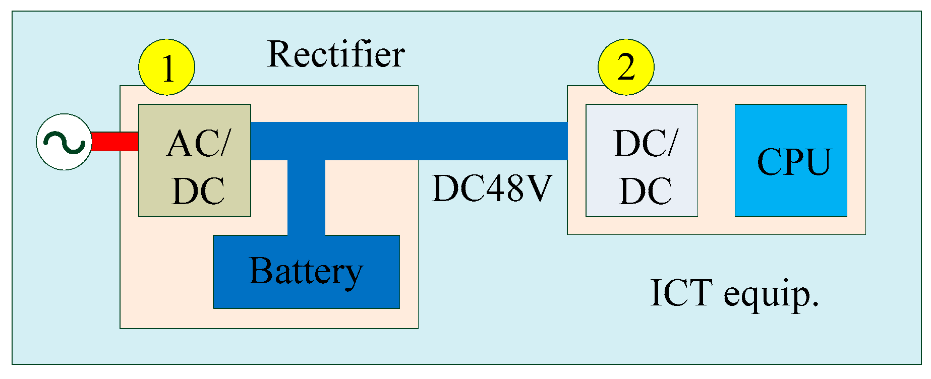
Over the years, the demands of computing and telecommunication have significantly increased along with the requirements of high efficiency and high power density due to the widespread deployment of information and communication technology (ICT) equipment [
1]. In general, ICT equipment uses a two-stage AC–DC converter, as shown in
Figure 1 [
2]. Then, the first stage converts the AC voltage supplied from the power grid into DC voltage (around 48 V) in telecommunication buildings, and the second stage uses a step-down DC–DC converter to supply suitable DC power for the components such as central processing units (CPUs), memory, hard disks, and servers, which use DC voltages of 1.8 V, 3.3 V, 5.0 V, and 6 V, respectively [
2,
3]. Moreover, the battery is used in ICT equipment as a backup power supply. Normally, the first stage provides isolation and high conversion efficiency, and the second stage is usually a non-isolated DC–DC converter due to its advantages such as simple structure, low cost, and high power density [
4,
5,
6,
7]. In this case, the conventional buck converter has been discussed for using in the second stage. However, this converter cannot operate well when the duty cycle is very small because the output voltage is highly variated with a small error of the duty ratio, and the output voltage cannot be regulated precisely, causing further problems for the devices [
8,
9,
10]. Therefore, many researchers have put great effort into studying how to increase voltage gain in step-down DC–DC converters. In addition, the high voltage stress on components (MOSFETs, capacitors) is another critical issue in high-voltage-gain circuits, since the input voltage is high [
11,
12]. High-voltage devices will have high on-resistance, high diode forward voltage, and high parasitic capacitance, which lead to high losses on the devices and affect the total efficiency of the circuit. Thus, the choice of components, their losses, and the cost are carefully considered.
In order to overcome these limitations, several kinds of step-down DC–DC converters have been recently proposed [
12,
13,
14], which have brought about many remarkable advantages. For instance, double voltage gain can be achieved in comparison to the conventional buck converter, and the voltage stress on the switches is only equal to half of the input voltage. The proposed converter in [
14] represents a potential candidate due to simple structure and low component count, as indicated in
Figure 2. In particular, its voltage gain can be adjusted with additional phases, which is the dominant characteristic in comparison to other topologies. The continuous conduction mode (CCM) and triangular conduction mode (TCM) operations with the fixed switching frequency of this topology were presented in [
14]; however, these operations suffer from some tradeoffs. When the converter operates in CCM, a high inductance is required, and a large size of the magnetic component is needed [
15]. Additionally, hard switching not only causes undesired voltage spikes but also reduces the total efficiency by increasing the switching loss. In TCM operation, the switching devices can achieve ZVS to reduce switching loss, and the inductor has a smaller size [
16]. However, the inductor ripple current keeps a constant value in the range of load, which leads to a high root-mean-square (RMS) inductor current at light load conditions and a large differential mode (DM) noise. As a result, low power conversion efficiency usually occurs. Introducing variable switching frequency into TCM operation can change the inductor ripple current, which can solve the issues in TCM with the fixed switching frequency, and the switches can still achieve ZVS [
17]. Moreover, many topologies, which use bulky resonant components to achieve ZVS, have been proposed to increase circuit efficiency [
18]. Applying TCM operation with variable switching frequency can help the switch obtain ZVS without additional components, which reduces the cost and increases the power density [
5].
In TCM operation, it is possible to turn off the low-side switch after the inductor current becomes negative, and the high-side switch can achieve ZVS. Normally, the energy transfer from the inductor to the output capacitances (
) of the switches can be used to explain the mechanism of ZVS, and the reverse inductor current should be enough for this mechanism [
7]. However, conventional MOSFETs have high parasitic capacitance, which causes low reverse inductor current. This leads to increase inductor ripple current, high core loss, and winding loss. Moreover, the higher parasitic capacitance will require a higher time to charge and discharge the parasitic capacitances, which leads to a higher dead-time duration for high-side and low-side switches. This is not applicable for high-frequency applications because of high duty cycle loss. Therefore, using wide-bandgap (WBG) devices can overcome these limitations. WBG devices, which have smaller parasitic capacitance, can help the converters increase the switching frequency and reduce the size of passive components such as inductors and capacitors [
19]. However, with the low gate-to-source threshold voltage, WBG devices lead to extreme noise sensitivity for the controller [
20]. Therefore, the circuit design needs to be carefully considered in high-frequency applications.
The energy method is just an estimation method in ZVS design, which does not give the exact ZVS condition [
7]. Thus, finding the correct reverse inductor current is one of the problems of TCM modulation in maintaining ZVS in the full range of load. In this paper, resonant analysis is specifically performed for deciding the ZVS condition. Consequently, the constant reverse inductor current and the required dead-time can be deduced. The basic TCM operation principle with variable switching frequency and ZVS conditions are explained in
Section 2. In
Section 3, the range of switching frequency and the required inductance values are also determined to enable TCM operation in the full range of power for the circuit. Moreover, this converter can be operated in both forward and reverse directions, which can be applied in other applications such as battery chargers in electric vehicles and solar energy systems with charging and discharging modes. Thus, all discussions in this paper are analyzed for both directions. Lastly, a 48 W high-voltage-gain bidirectional DC–DC converter prototype with GS61008T is implemented to verify the analysis, which is shown in
Section 4. The paper is summarized and concluded in
Section 5.
2. Analysis of ZVS Condition
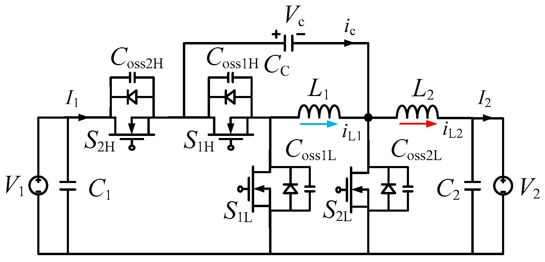
In
Figure 2, the voltage
and the current
are regulated by the main switches
and
in the forward direction, whereas the voltage
and the current
are regulated by the main switches
and
in the reverse direction. Additionally,
and
are the inductor currents in inductors
and
in forward mode, respectively. The gate-to-source voltages of
and
are shifted by
, and the signals of switches
and
are complementary with the signals of switches
and
, respectively. The clamping capacitor
, which is designed to maintain the voltage (
with low ripple at steady state, has the important role of increasing the voltage gain and reducing the voltage stress of switches to (
except switch
, as shown in
Figure 3. The voltage in the capacitor
does not contribute to reducing voltage stress of the switch
in
. Therefore, the voltage stress of the switch
is equal to
in this interval and equal to (
in the remaining intervals.
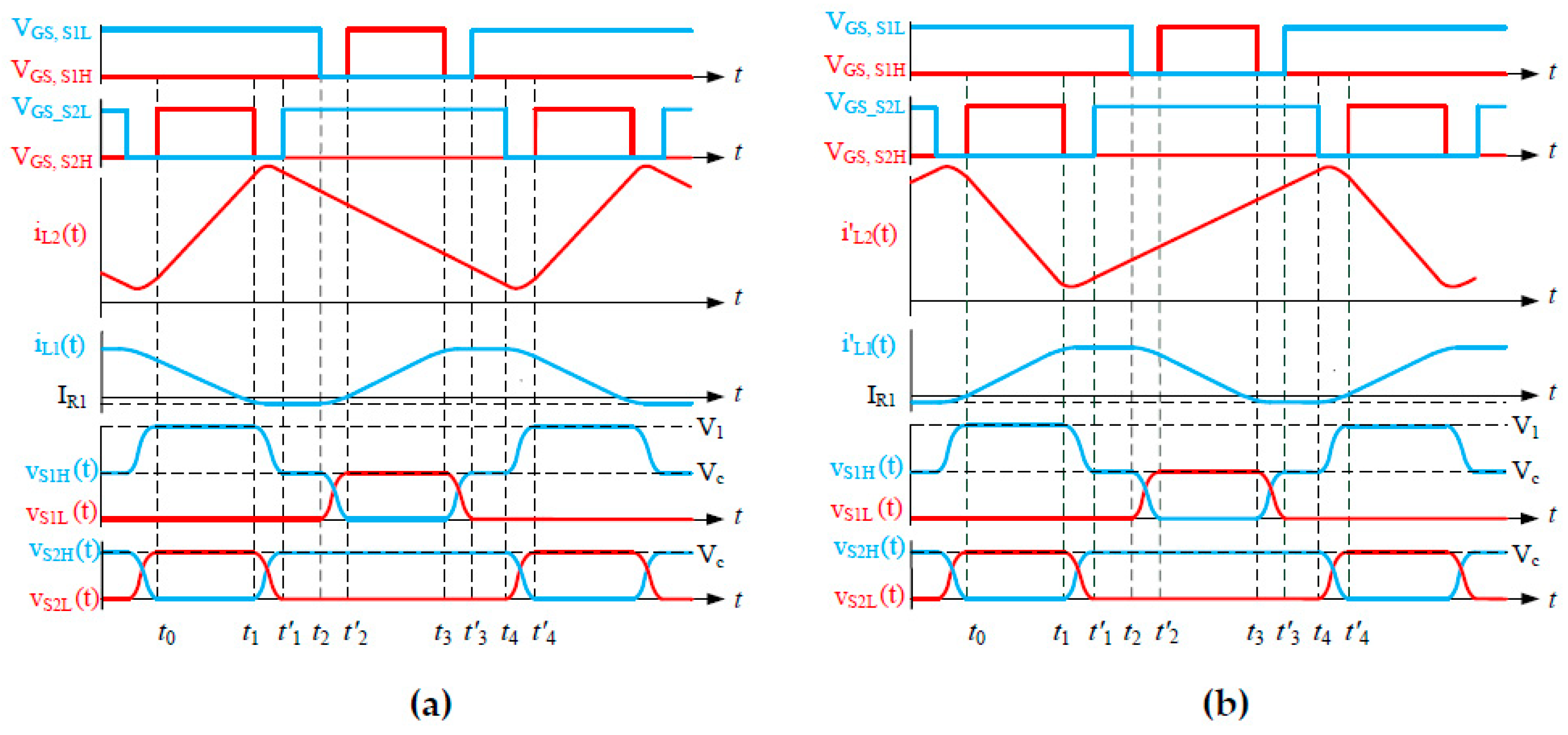
There are eight time intervals in one switching cycle, as shown in
Figure 3. The time intervals
,
,
, and
are the same with CCM operation. This paper only focuses on analyzing resonant periods
,
in the forward direction and
in the reverse direction to determine the reverse inductor current
and the required dead-time duration for all switches. The key waveforms during one switching cycle and the states of switches in every resonant period are indicated in
Figure 3 and
Figure 4, respectively. In the reverse direction,
and
have the same magnitude and the opposite direction with
and
, respectively, as shown in
Figure 3b. The parameter
is the gate-to-source voltage of the switch, and
are the voltages in output capacitances of switches
and
, respectively.
In the resonant analysis, two assumptions to simplify the analysis are that the output parasitic capacitance of the switch keeps a constant value, and the body diode voltage drop of the switch is neglected.
2.1. In Buck Direction (Forward Direction)
At the time
, the inductor current
is
, switch
turns off, and the inductor
resonates with the output parasitic capacitances of
and
, increasing
and reducing
, as presented in
Figure 3a and
Figure 4b. At the time
,
increases to
,
decreases to zero, and
turns on to achieve ZVS, as shown in
Figure 3a. The derivation process to achieve ZVS of the switch
is similar. When the converter operates at a high switching frequency, setting redundant dead-time
to achieve ZVS leads to large duty cycle loss. Thus, the resonant periods
and
were analyzed to determine the dead-time for switches
and
.
2.1.1. Resonant Period (
The initial circuit during the resonant period is indicated in
Figure 5a,b is the equivalent circuit with Laplace transforms. At the time
, the current value in the inductor
gets minimum value
, the voltage values of switches
and
are
and zero, respectively, and the voltage source
has already been considered in the initial voltages of switches
and
at the time
.
From
Figure 5b, the voltage of the main switch
in the s domain is expressed as
According to Equation (1), the voltage
during the resonant period can be derived.
where the equivalent capacitance
, the characteristic impedance
, and the resonant frequency
.
From Equation (2), the switch
gets ZVS when
Thus, the value of the reverse inductor current can be determined.
From Equation (4), the maximum value of
can be determined at the quarter of the resonant period. Thus, the minimum dead-time for the switch
is defined as
2.1.2. Resonant Period (
The initial circuit at the time
is expressed in
Figure 6a. Using Norton’s theorem, the voltage
in series with the inductor
can be represented as the current source
in parallel with the inductor
, as illustrated in
Figure 6b. After that, the current source in parallel with inductors
and
can be replaced by the voltage source
in series with the inductor
, as indicated in
Figure 6c.
Figure 6d is the equivalent circuit with Laplace transforms. At the time
, the currents
and
are zero and
, and the voltage values of switches
and
are
and zero, respectively.
From
Figure 6d, the voltage of the main switch
in the s domain is expressed as
According to Equation (6), the voltage
during the resonant period can be derived as
where the current I is equal to
, the equivalent inductance
,
, the characteristic impedance
, and the resonant frequency
.
Consequently, the ZVS condition for switch
is described by Equation (8).
The peak current of the inductor
can be expressed as
From Equations (8) and (9), the ZVS condition for the switch
is
where
is the ripple current of the inductor
.
where
is the switching frequency of the converter.
2.2. In Boost Direction (Reverse Direction)
The operating principle of the reverse direction is similar to the forward direction, as indicated in
Figure 3b. Therefore, the resonant analysis of the reverse direction is not repeated for conciseness. The ZVS conditions of the main switches
,
in boost direction during resonant periods are shown below.
In the resonant period (
, the voltage of the main switch
is expressed as
Consequently, the ZVS condition of switch
is described by Equation (13).
In the resonant period (
, the voltage of the main switch
is expressed as
Consequently, the ZVS condition for the switch
is described by Equation (15).
3. Switching Frequency Calculation
Using the inductor volt-second balance, the equations for the ripple currents
, and the switching frequency
are expressed in Equations (16)–(18).
In Equations (16) and (17), when the output power is reduced and the reverse inductor current remains constant, the ripple currents and are lower. Thus, the RMS currents of both inductors will be reduced at light load, which leads to a reduction in conduction loss in the inductors.
In Equation (18), clamping capacitor voltage and duty cycle D are constant. Therefore, the switching frequency has to be changed following the current to maintain the constant reverse inductor current , which helps all switches to obtain ZVS.
The ZVS conditions of all switches in Equations (4), (10), (13) and (15) depend on the constant reverse inductor current
. Thus, only the inductor
must operate at TCM, and the inductor
can operate at CCM to reduce the current stress in the output capacitor. Therefore, the inductance
can be less than the critical inductance
and the inductance
can be greater than the critical inductance
, as shown in Equation (19).
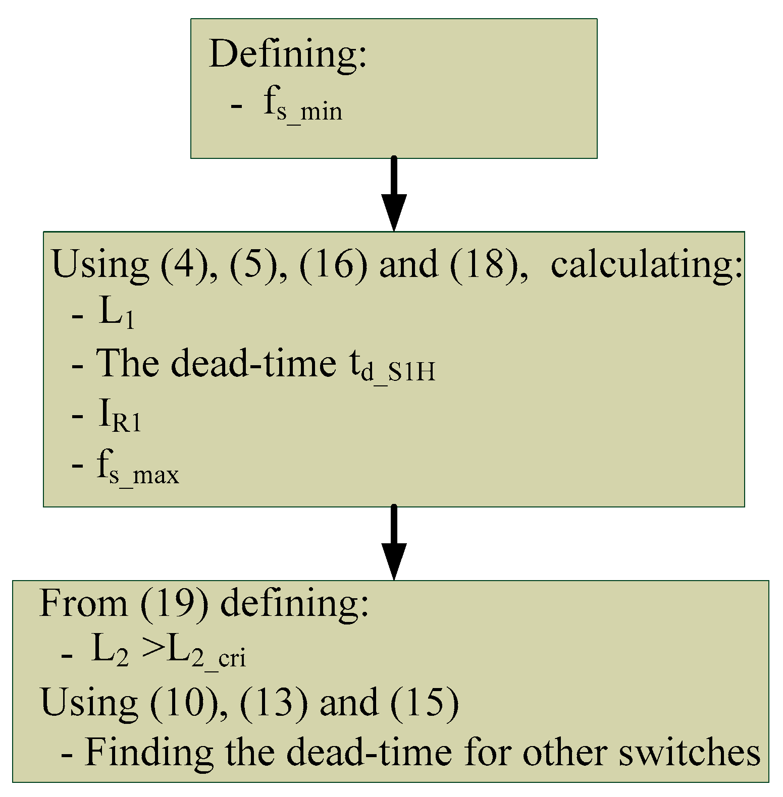
The inductances
,
, the dead-time for all switches, the reverse inductor current
, and the range of switching frequency can be determined using the steps in
Figure 7. In addition, the inductance
can be selected to be greater than
, as long as the converter can meet the expected power density and cost.
4. Experimental Verification
In order to validate the ZVS conditions, a high-voltage-gain bidirectional DC–DC converter was built with 48 W output power. The circuit was designed to work in TCM operation, and the switches could achieve ZVS in the full range of output power. The 100 V GaN device GS61008T from GaN Systems, which has low output capacitance, was implemented in the converter.
In addition, the nonlinear parasitic capacitance of the switch should be considered in the ZVS condition for higher accuracy. Due to this nonlinearity, the charge
stored in parasitic capacitances
is also a function of the applied voltage
. Therefore, a corresponding equivalent parasitic capacitance
could be obtained to exhibit the same amount of stored charge as the nonlinear capacitance [
21]. The blue line in
Figure 8 indicates
versus
as in the datasheet of GS61008T [
22], while the red line presents the relationship between
and
.
The minimum operating frequency in the converter is 200 kHz at full load, and, following step 2 in
Figure 7, the inductance
and the dead-time
were calculated to be around 3.1 μH and 150 ns, respectively. According to step 3 in
Figure 7, the remaining switches had 100 ns dead-time, and the maximum operating frequency of the converter was 700 kHz at 20% output power.
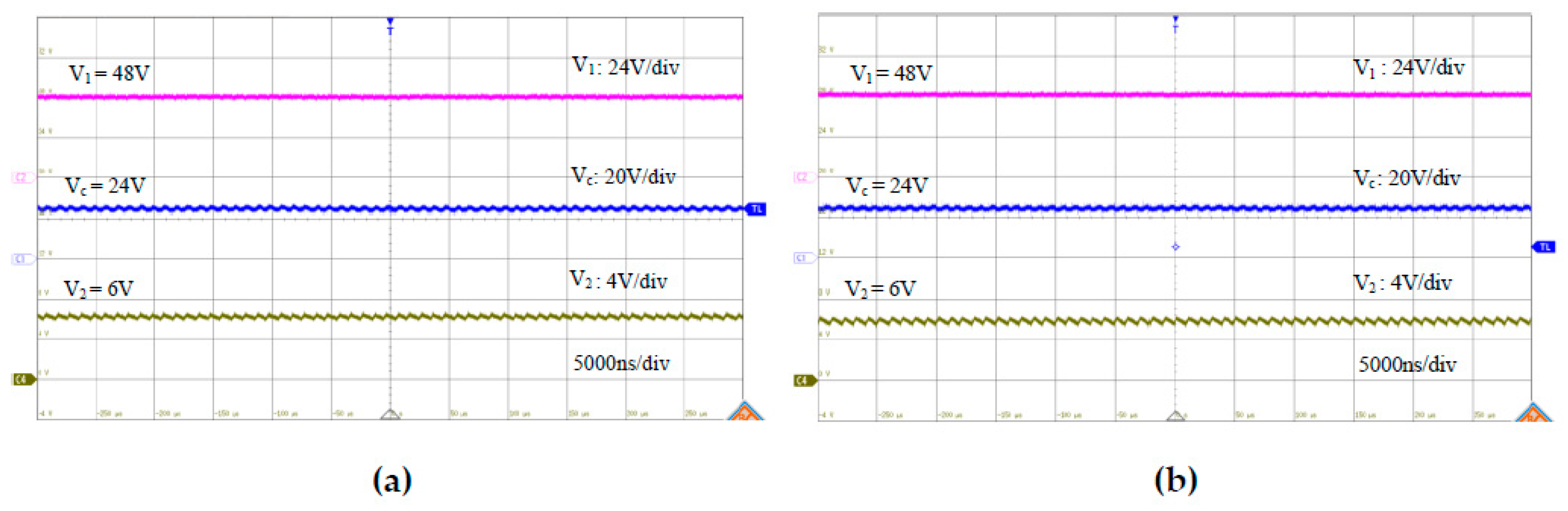
The clamping capacitor should have a large enough capacitance to reduce the voltage ripple.
To ensure constant voltage on the clamping capacitor, the value of
should be selected as double the calculated value to avoid the derating issue. The clamping capacitor voltage
, the voltage
, and the voltage
waveforms are shown in
Figure 9 for both directions, and
was kept constant at half of
. The key parameters and components are summarized in
Table 1.
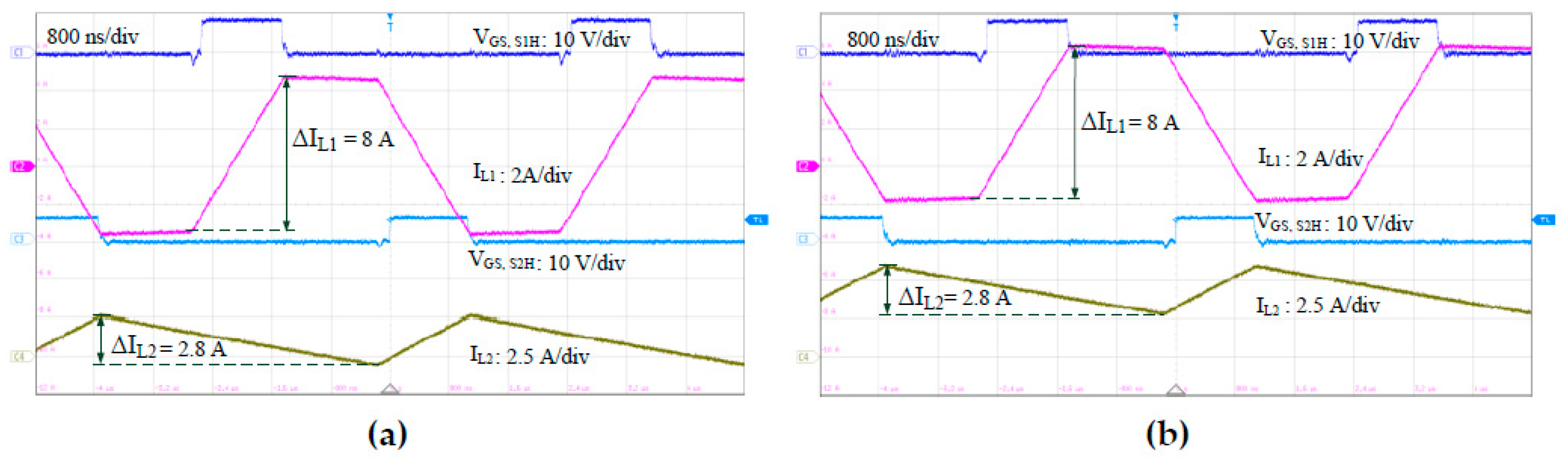
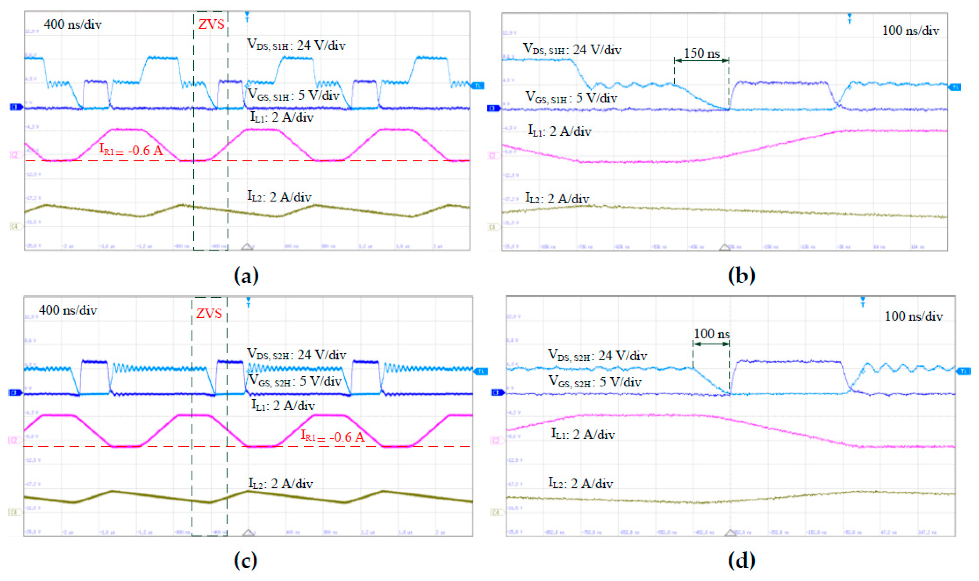
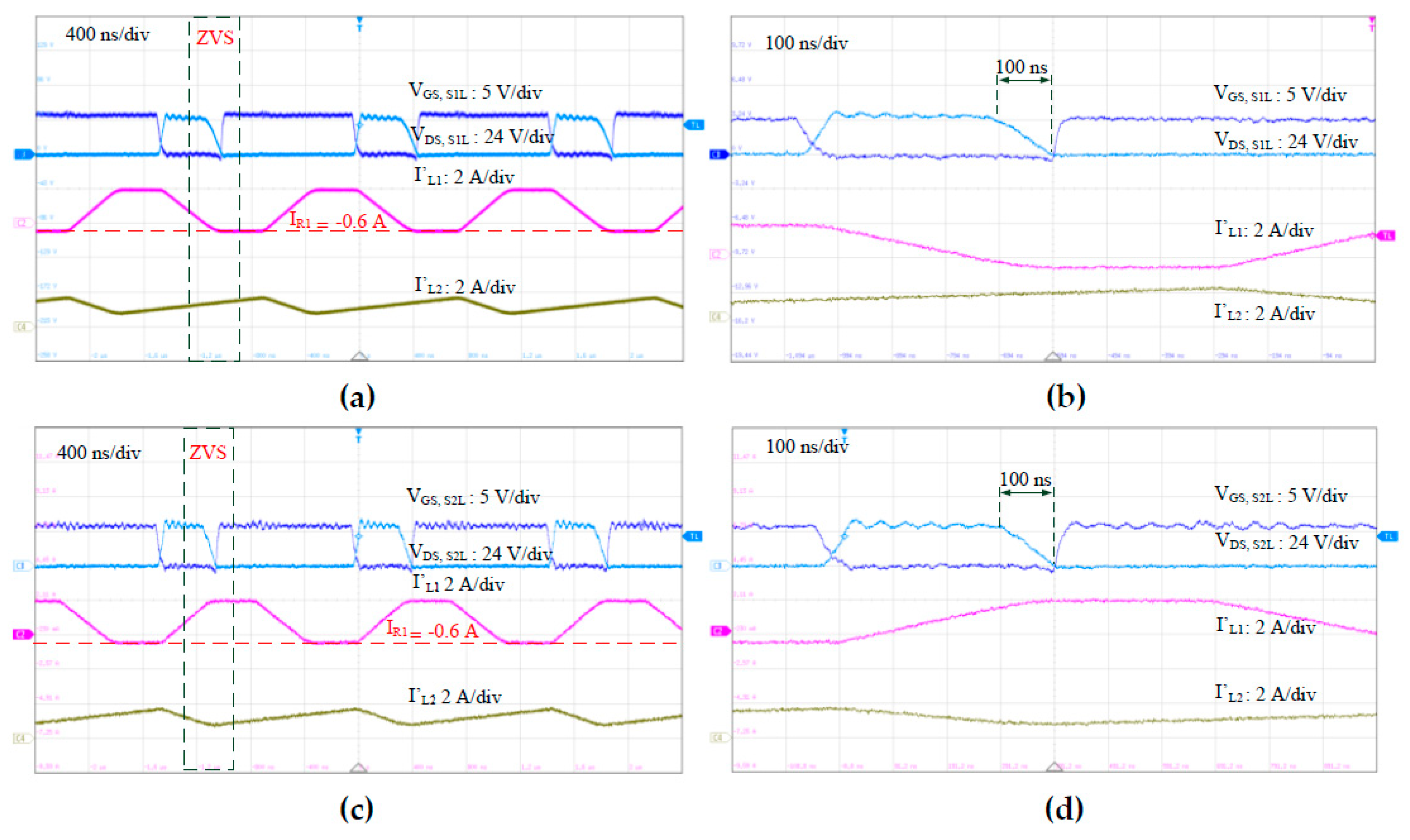
The inductor current waveforms at 20% load and 60% load in the forward direction are shown in
Figure 10 and
Figure 11, respectively. In
Figure 10, the converter operated in TCM with the variable switching frequency, while the reverse inductor current
was kept constant at −0.6 A. Moreover, comparing to TCM operation with fixed switching frequency in
Figure 11, the ripple currents of both inductors at 20% load and 60% load were reduced around 71% and 34%, respectively. Therefore, the winding loss and core loss of inductors, and the conduction loss of switches were reduced, which helped to improve the total efficiency of the converter. In the reverse direction, the ripple currents would have the same results. All switches in the converter could achieve ZVS in the full range of load, as shown in
Figure 12 and
Figure 13.
For the traditional interleaved two-phase bidirectional DC–DC converter, the ZVS condition for the switch of each phase depends on its reverse inductor current [
23]. However, in this topology, the reverse current in the inductor
can control all ZVS conditions for all switches, as shown in
Figure 12 and
Figure 13. Hence, the current balancing issue is not a great deal in this topology, and it is beneficial for designers to select the inductors in this circuit.
Figure 14 shows the efficiency in both flows. When the output power was reduced, the efficiency of the converter in TCM operation with variable frequency was higher than that in TCM operation with fixed frequency due to the reduction in peak-to-peak current in both inductors. The converter obtained the highest efficiency of 97% and 96.8% in the forward direction and the reverse direction, respectively.
Figure 15 shows the hardware of the high-voltage-gain bidirectional DC–DC converter.


