Article

Comparison of Different Large Signal Measurement Setups for High Frequency Inductors

Power Electronics Systems Group (GSEP), Department of Electronic Technology, Carlos III University of Madrid, 28911 Leganés, Spain
*
Author to whom correspondence should be addressed.
Electronics 2021, 10(6), 691; https://doi.org/10.3390/electronics10060691
Submission received: 2 March 2021 / Revised: 10 March 2021 / Accepted: 13 March 2021 / Published: 15 March 2021
(This article belongs to the Special Issue High-Frequency Power Converters)

Abstract

:
The growing interest of miniaturized power converters has pushed the development of high frequency inductors integrated in Power Supply on Chip or Power Supply in Package. The proper characterization of inductor impedance is a challenge due to the dependence of the impedance on the current, the high quality factor (Q) and the high frequency range where these devices operate. In this paper, we present a comparison of different measuring methods to characterize high frequency and high Q inductors. The comparison is based on a systematic analysis of the measurement process, quantifying the influence of the parameters that affect the measurement result. Four common measurement setups are analyzed and compared. To validate the calculations, the resistance of a high frequency, high-Q inductor is characterized using every presented setup. The good match between calculations, simulation and measurement validates the analysis and the conclusions extracted.

1. Introduction

In recent times, different measurement techniques have been applied for the large-signal characterization of inductors working at high frequency. This kind of test is especially critical in applications where manufacturing the component is very expensive, complicated or is very affected by manufacturing tolerances. In these cases, a precise knowledge of both the inductance and the losses of the magnetic component would play an important role in the development of the circuit, as they have an impact on the current ripple and the converter efficiency.
The characterization of the magnetic component impedance using network analyzers is widely used to measure its inductance and resistance. However, this test provides limited knowledge of the component, since it is done in small-signal, and the performance of the magnetic component working in the actual converter could be very different. On the one hand, this is because of the lack of DC current through the inductor. On the other hand, the current ripple through the component clearly affects its performance in the B–H curve, yielding modifications in the inductance and the resistance compared to the values obtained through the small-signal test.
There has been a significant number of reports on large signal characterization of discrete passive devices. In the particular case of characterization of inductors, there is an increasing interest because of the thin film components working in Power Supply on Chip or Power Supply in Package [1,2,3,4,5,6,7,8]. These kinds of applications present two main challenges regarding the measurement: (1) the high frequency (above 10 MHz) and (2) the high Q of the component (very small resistance compared to its reactance). Since the purpose is to perform large-signal measurements, most presented techniques differ in the method of measuring the voltage across and the current through the component [3,9,10,11]. There are also some proposals focused on the measurement of the losses using calorimeters [12]. The main problems associated with these methods are the long tests and the difficulty of sensing temperature variation when the resistive part is very small and so is the loss.
This work is focused on the comparison of different large-signal measurement methods using voltage and/or current probes and an oscilloscope. In a conventional approach [9], the current is measured using a voltage probe to sense the voltage across an auxiliary resistor. In [3,13], the measurement was performed using a voltage probe and a current probe. In [10], different reactive components are placed in series with the device under test (DUT) to measure the core loss in high frequency coupled inductors. In [11,14], the series component is a capacitor, the value of which is calculated in such a way that the resonance frequency of the capacitor and the inductor is as close as possible to the frequency of the test. However, the most appropriate method is not clearly determined since it depends on the device under test and its testing conditions (current amplitude and frequency).
To provide a fair comparison between characterization techniques, a figure of merit is needed. One of the most common approaches to ascertain the validity of a measurement method is by analyzing the error, the uncertainty, or other statistical measure of the deviations of the obtained results [15,16,17,18,19,20,21,22]. Many of the mentioned published measurements fail to provide a proper quantification of this deviation [1,2,3,9]. Others only deal with the uncertainty due to the phase error [13,14,23], neglecting the magnitude error, which may be important, for instance, when measuring near resonance. In some cases, most effects are taken into account [9,10,24], but the analysis is performed on transformers or coupled inductors. Consequently, no comprehensive analysis has been carried out about the deviation in the characterization of single inductors, which is the main contribution of this work.
On top of that, even when an estimation of the accuracy of a measurement is provided, in most cases the statistical distribution of the uncertainties is needed. This knowledge is often not given by the manufacturers and has to be assumed [18]. To avoid such problems, sometimes a Monte-Carlo analysis is performed, using simulation models of the magnetic component under test and the instrumentation. This approach relies on statistical calculations that can result in a large number of iterations to achieve a good estimation [22], which is very time and resource consuming.
The contribution of this work is to provide a worst case analysis of some of the reported large-signal measurement techniques in the state-of-the-art, taking into account not only the technique itself but also how the results are affected by the tolerances of the probes, the oscilloscope and the additional components included in the measurement. The main innovation is to present a quantitative tool to optimize or select the most appropriate measurement technique, in terms of the available instrumentation and the characteristics of the measurement (frequency, expected impedance, etc.).

2. Measurement Setups

The complex impedance of an inductor ( Z L ̲ ) at a frequency f can be modeled as an inductance L in series with a resistance R L , which accounts for all the different losses lumped together:
Z L ̲ = 2 π f L i + R L = Z L Φ L ,
where Z L and Φ L are the module and phase of the impedance, respectively.
For the characterization of the complex impedance of the inductor using an oscilloscope, it is required to measure two signals: inductor current I L ̲ and inductor voltage V L ̲ . The inductor impedance can then be calculated using (2).
Z L ̲ = V L ̲ I L ̲ .
Notice that, since the impedance is defined at a certain frequency, voltage and current are expected to be sinusoidal signals at that frequency, which is why they are modeled as phasors.
For the current measurement, two different techniques can be employed: direct sensing of the current I L ̲ , using a current probe; and indirect current sensing, measuring it as the voltage drop V S ̲ across a known sensing resistor R S , following expression (3):
I L ̲ = V S ̲ R S .
When measuring the voltage V L , two techniques are widely used: direct voltage sensing on the inductor, and indirect voltage sensing, where a capacitor is added in series and the combined voltage is measured.
The four different setups for the measurement of voltage and current are displayed in Figure 1. The configurations where the current is measured using a current probe are setups 1 and 3 (Figure 1a,c), while a voltage and a sensing resistor are used in setups 2 and 4 (Figure 1b,d). Regarding the voltage sensing, the top row (a and b) corresponds to the direct measurement on the impedance, whereas the bottom one shows the setups where a capacitor ( C E ) is added in series and the combined voltage V L E is measured.
Since two of the studied setups shown in Figure 1 employ an extra capacitor, the complex impedance of the combined inductor and the external capacitor Z L E ̲ , can be calculated by:
Z L E ̲ = Z L ̲ + Z C E ̲ = Z L E Φ L E ,
where Z L E and Φ L E are the module and the phase of the impedance, respectively, and Z C E ̲ is the impedance of the additional capacitor. In the setups where no capacitor is used, its impact is not present and Z L E ̲ = Z L ̲ .

3. Modeling the Measurement Accuracy

In this section, the method to analyze and compare the measuring setups is presented. The basic idea is to assess the impact on the measurement results of different parameters: probe tolerances, sensing resistor tolerances, discretization effects, etc.
The first step of this analysis is to identify the relationship between the measured quantity F and the parameters that affect the measurement ω i , defined in expression (5):
F = f ( ω 1 , ω 2 , ω 3 , ) = f ( ω i ) ,
Equation (5) allows evaluating the propagation of the variation of the parameters ω i to the value of F. The function f can be nonlinear and in general is difficult to handle. In order to calculate how small variations of parameters ω i affect the measurement F, the function f is analyzed applying the first order Taylor series approximation (6) in the vicinity around a given value F 0 , considering the variations of parameters ω i around the values ω i , 0 :
F = F 0 + f ω i ω i ω i , 0
where partial derivatives are obtained for F = F 0 and ω i = ω i , 0 . Expression (6) can be rewritten considering the variations of F and ω i around F 0 and ω i , 0 , respectively:
ϵ F = F F 0 = f ( ω i ) f ( ω i , 0 ) ; ϵ ω i = ω i ω i , 0 .
yielding expression (8):
ϵ F = f ω i ϵ ω i .
Expression (8) can be used for different purposes. On the one hand, to assess the maximum possible variation of the measurement results, i.e., the maximum value of ϵ F , expression becomes (9), which corresponds to the worst case, limiting error or worst case uncertainty [25].
ϵ F m a x = f ω i ϵ ω i , m a x .
Expression (8) can also be used to assess the uncertainty in the measurement, according to the definitions and procedures published in the Guide to the expression of uncertainty in measurement [15]. If the parameters ω i are characterized by an appropriate probability distribution, and ϵ ω i are the deviations from the mean or expected value ϵ ω i = ω i E [ ω i ] , expression (8) can be used to derive the uncertainty of F as defined in (10):
σ F = f ω i 2 σ ω i 2 ,
where σ F is the uncertainty of the measurement F and σ ω i 2 is the variance of the parameters ω i . In this case, all ω i are assumed independent and therefore the covariance is 0.
In this work, the approach defined in expression (9) is adopted, because the goal is to compare different measurement setups in terms of the worst case. This comparison only requires the knowledge of each parameter limits, but not its probability distribution.
The value of ϵ F depends on the value of F 0 and ω i , 0 , since the partial derivatives in (6) and (8) are calculated for these values. If F 0 were the real value F r e a l , the estimation of the worst case would include all the possible values of the measurement F m e a s . However, if F 0 were the measured value F m e a s , the estimation of the worst case would include the real value only if ϵ F m e a s , m a x ϵ F r e a l , m a x (Figure 2). F r e a l is actually unknown but, in a practical case, F r e a l and F m e a s are close, so the assumption ϵ F m e a s , m a x ϵ F r e a l , m a x is reasonable. Following this principle, when a measurement F m e a s is obtained, the real value F r e a l must be within the interval determined by the worst case approach. This way, the real value is ensured to be between two symmetrical limits:
F m e a s ϵ F m e a s , m a x F r e a l F m e a s + ϵ F m e a s , m a x .
Terminology is essential when discussing metrology problems, and terms such as error or uncertainty have been defined in international documents as [15,16]. The aforementioned maximum variation of the measurement ϵ F m e a s , m a x or variation of the parameters affecting the measurement ϵ ω i , m a x , with respect to their nominal values F m e a s and ω i , m e a s , will be referred in this work as deviation of measurement results ϵ F or deviation of the parameters ϵ ω i . The quantities F to be measured are L and R L , and the different measurement setups are compared in terms of ϵ L and ϵ R L . The lower the value of ϵ L and ϵ R L , the better the measurement setup.

4. Worst Case or Maximum Deviation of the Measurement
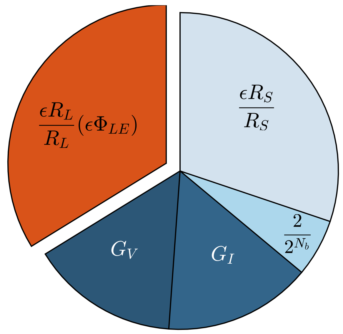
As mentioned before, when characterizing an inductor with an oscilloscope, there are two signals that have to be measured: voltage and current. Both of them have some deviations in amplitude and phase that contribute to the total deviation on the inductance ϵ L and the total deviation on the resistance ϵ R L . Since the oscilloscope makes time measurements, the time deviation has to be considered in the analysis as well.
When characterizing high Q inductors, the value of L usually has a very small deviation associated, but that is not the case for the value of R L , deviation of which can be very high. From the measurements of magnitude and phase of the impedance Z L E ̲ , the resistance value R L can be extracted using (12),
R L = Z L E cos Φ L E .
Note that in this analysis the parasitic resistance of C E capacitor has been neglected for the sake of simplicity, but it can be easily added following the proposed procedure.
The deviation of R L , is defined as (13):
ϵ R L = R L Z L E ϵ Z L E + R L Φ L E ϵ Φ L E .
The normalized value of the resistance deviation is then calculated as (14).
ϵ R L R L = cos Φ L E R L ϵ Z L E . 7 e m ϵ R L R L ( ϵ Z L E ) + tan Φ L E ϵ Φ L E . 7 e m ϵ R L R L ( ϵ Φ L E ) .
As can be seen, the total deviation depends on the deviation of the phase and the deviation of the module, which can be analyzed separately.

4.1. Deviation of R L Due to ϵ Φ L E

When using an oscilloscope, only the time and voltage or current values of a signal can be acquired. From the time measurements, periods, frequencies and phases can be calculated. The phase Φ L E is obtained from the time delay between current and voltage ( Δ T ) and the period T of the measured signals, by means of (15). Notice that in setups 1 and 2 (Figure 1) Φ L E is equal to Φ L , since no additional capacitor is used.
Φ L E = Δ T T 360 .
The deviation of Φ L E is defined as
ϵ Φ L E = Φ L E Δ T ϵ Δ T + Φ L E T ϵ T ,
which translates into
ϵ Φ L E = 360 T ϵ Δ T + Δ T · 360 T 2 ϵ T .
When making a time measurement with an oscilloscope, the maximum deviation is imposed by its sample rate f S [10]. In (17), since both deviations ( ϵ Δ T and ϵ T ) come from time measurements, their maximum values can be calculated as
ϵ Δ T = ϵ T = 1 f S .
The term of the maximum normalized deviation of R L (14) that depends on Φ L E can now be rewritten as:
ϵ R L R L ( ϵ Φ L E ) = tan Φ L E · 1 f S 360 T + Δ T · 360 T 2 .
The problem when making such measurements on a high Q inductor can be easily identified from (19) [14]: for a phase close to 90º, the tangent tends to , which would cause ϵ R L to tend to as well, even if the deviations of the measured phase were small.

4.2. Deviation of R L Due to ϵ Z L E

The module Z L E , obtained from the measurements of current and voltage amplitudes, can be calculated by means of (20). This expression is used for every measurement setup shown in Figure 1. The first equality is employed if the current is measured using a current probe (Figure 1a,c), and the second one in the setups that include two voltage probes (Figure 1b,d).
Z L E = V L E I L = V L E V S / R S .
The deviations of the impedance module can then be modeled as:
ϵ Z L E = Z L E V L E ϵ V L E + Z L E V S ϵ V S + Z L E R S ϵ R S .
By means of (21), the term of ϵ R L / R L that depends on the deviation on the impedance module ( ϵ R L / R L ( ϵ Z L E ) ), presented in (14), can be rewritten as (22). If a current probe is used, there is no sensing impedance, and that term is omitted. In contrast, if the current is measured using a voltage probe, the deviation is composed of two terms: deviation due to the probe and deviation due to the sensing resistor R S :
ϵ R L R L ( ϵ Z L E ) = G V + 1 2 N b 7 e m Voltage measurement + G I + 1 2 N b 6 e m Current / voltage probe + scope + ϵ R S R S 6 e m Sensing resistor 10 e m Current measurement .
where G V is the per unit deviation of the voltage probe gain, G I is the per unit deviation of the current probe gain, N b is the number of bits of the oscilloscope ADC and ϵ R S / R S is the per unit deviation of the sensing resistor.

4.3. Discussion

By means of equations (19) (deviation of R L due to the deviation in the phase) and (22) (deviation of R L due to the deviation in the module), Equation (14) can be rewritten as (23):
ϵ R L R L = G V + 1 2 N b + G I + 1 2 N b + ϵ R S R S . 7 e m ϵ R L R L ( ϵ Z L E ) + tan Φ L E · 1 f S 360 T + Δ T · 360 T 2 7 e m ϵ R L R L ( ϵ Φ L E ) .
Equation (23) provides crucial insight to the total deviation of the inductor measured resistance ϵ R L . It allows the designer not only to calculate the worst case, but also to analyze which parameter of the measurement contributes the most to it. Thanks to this, the deviation can be reduced in the most efficient way:
  • If Φ L E 90 º, for instance when measuring a high Q inductor without an additional capacitor, the main driver of the deviation on R L is the term related to the phase (19). The main contributor in that term is the sample rate of the oscilloscope ( f S ) and the normalized deviation produced by it depends on the period T at which the inductor is being characterized. Therefore, to improve the results, the only options are either to measure at a lower frequency or to employ an oscilloscope with a higher sample rate.
  • If the measurement is done by adding a capacitor to compensate the reactance Φ L E 0 º. In this case, the main driver of the deviation on R L is related to the module, and the three terms that have to be taken into account are the ones shown in (22):
    -
    The vertical resolution of the oscilloscope, given by the number of bits of its ADC ( N b ) is always present, whether the current measurement is done using a current probe or a voltage one. To minimize its impact, a high number of bits is required.
    -
    The nominal deviation on the gain of the probes used to measure the voltage ( G V ) and current ( G I ) has the same impact. However, active voltage probes usually have a better performance than current ones ( G V < G I ), but the impact on the deviation of a sensing resistor ( ϵ R S ) can increase the deviation ϵ R L , and even make it a worse option.
Figure 3 shows an example of the distribution of the deviations in R L , in orange the term related to the phase deviation (19) and, in blue, the four terms that comprise the deviation due to the module (22). The numerical results are summarized in Table 1. The calculations were performed for a measurement taken with two voltage probes and a series capacitor to drive the phase close to 0º, corresponding to Setup 4 (Resonance VV) in Figure 1. The inductor and equipment used for the example are the ones that are going to be used later to perform the measurement, summarized in Table 2 and Table 3.
For this particular example, the normalized total deviation on the value of the measured R L is 3.3 % . As can be seen, since the phase Φ L E has been driven close to 0º by adding a series capacitor, most of the deviation in ϵ R L comes from the deviation in the impedance module ϵ Z L E . Inside this term, the main driver is the deviation due to the sensing resistor, which accounts for the same as the two voltage probes combined. Thanks to the use of a high-resolution oscilloscope (with a 10 bit ADC) the impact of this term is reduced to only a 0.2 % deviation on the value of R L .
This distribution highlights the importance of taking into consideration not only the terms related to the deviation on the phase, but also the ones related to the module. The lower the value of the phase Φ L E , the higher the relative impact of these terms, which end up being the main deviation drivers when measuring close to the resonance frequency Φ L E 0 .
As mentioned in the introduction, the quantitative analysis of the distribution of the deviation allows the optimization of the measurement system. In this example, improving the phase characterization ( Φ L E ) by increasing the sample rate and/or by using a better calibrated R S will have the most significant impact on the quality of the measurement. On the other hand, increasing the number of bits of the oscilloscope’s ADC will barely have an impact on the results.

5. Results

To validate the proposed analysis, the measurement of an inductor was simulated and then performed in a laboratory. To emulate a real scenario, a high Q inductor was tested at high frequency (13.45 MHz). Its characteristics, provided by the manufacturer, are summarized in Table 2.

5.1. Validation by Simulation

To validate that the provided procedure allows the calculation of the worst case scenarios, a sensitivity analysis was carried out and its results compared with the theoretical limits. The sensitivity analysis consists of sweeping every possible combination of the maximum and minimum values of the considered parameters. These limit values are given by their tolerance, obtained from the manufacturers datasheets and summarized in Table 3. The circuit used for the simulation of every setup, with the added limits for every component, is shown in Figure 4:
  • The tolerances in the value of R S and C E ( ϵ R S and ϵ C E , respectively) are accounted for by adding or subtracting its value to the nominal one.
  • The tolerance in the gain of the probes and the deviation due to the bit resolution of the oscilloscope ( G x and 1 / 2 N b in (22)) are lumped together in ϵ V x and ϵ I x , the values of which are added or subtracted to the measurement of every probe.
  • The time deviation due to the sample rate of the oscilloscope has two different effects (18): the deviation of the real period of the measured waves, which is modeled as a deviation of the generator period ( ϵ T ), and the deviation of the phase of the two probes, modeled by a delay block in each of them.
Notice that the error due to possible delays among the probes is neglected. The reason is that a calibration and deskew of the probes has to be performed at the beginning of the test.
The four presented measurement setups are analyzed using the oscilloscope, the current probes and the active voltage probes indicated in Table 3. However, for setup 1 in Figure 1a (direct measurement of voltage and current on the inductor), a variation was considered: voltage measurement using passive voltage probes.
To emulate the measurement taken in a laboratory with an oscilloscope, only the waveforms of voltage and current are obtained from the simulations. From those waveforms, the values of magnitude and phase are calculated and the resistance is obtained using the equations given in Section 4.
The results of the sensitivity analysis for the four presented setups (Figure 1), and the additional study for setup 1 using a passive voltage probe, are shown in Figure 5. In the figure, the red dashed line is the real value of R L , called R L , n o m (known, since it is a simulation); the vertical blue lines represent the theoretical limits for the measured resistance in every setup [ R L , n o m ϵ R L , R L , n o m + ϵ R L ] , predicted by the equations given in Section 4; the yellow dots represent the calculated resistance values, obtained from the simulations of every combination of parameters.
As can be seen, the worst cases (the yellow dots that drift the most from the nominal value) match the predicted values (extremes of the blue lines). This validates the procedure of finding the interval in which every measurement would be for a particular real value. The small differences between analytical results and simulation for the last two measurement setups are assumed to be due to the non-linearity when calculating the deviation (9), due to the first order Taylor approximation.
As expected, setups where no capacitor is added to compensate the reactance (Direct IV (passive V), Direct IV and Direct VV in Figure 5) show the worst results for the measurement of the resistance of a high Q inductor. For all of them, the deviation of the measurement is more than five times the nominal value (186 m Ω ) and, although it lowers when using active probes, it still can result in negative resistance values. As analyzed in the previous section, this comes from the deviation imposed by the tangent tending to in (19), which cannot be avoided even if the components or the probes are improved.
In the last two setups, the results improve greatly when adding a capacitor in series with the inductor. Since the phase of the impedance can be driven close to 0, the deviation on R L can be estimated using (22), where every element depends solely on the components and devices used for the measurement. As shown, both setups (current and voltage probes or two voltage probes), have a similar performance, since the reduction of deviation provided by the active voltage probe (Table 3) is mostly shadowed by the deviation added by the sensing resistor.
Consequently, these simulation results validate the presented analysis.

5.2. Experimental Validation

The next step is to measure a real inductor, to check if the measurements match the simulations. The measurements were done with the same components and equipment used for the simulations, as shown in Table 2 and Table 3. The experimental setup, with and without probes, is depicted in Figure 6.
For every setup, a number of measurements are made and, for all of them, the resistance value is calculated. Since the procedure to obtain the range for the real value of the measured resistance was validated in the previous step, that range is calculated for every resistance measurement taken with every setup.
In Figure 7, an example of the process is shown for the setup that employs a current and a voltage probe, along with a capacitor to compensate for the inductor reactance (Resonance IV, Figure 1c). In the figure, every measurement is shown as a purple dot, with its associated deviation as a thin vertical orange line. To reduce the amount of data displayed in the next figures, every deviation is condensed into a single thick vertical bar, with its worst cases defined as the worst cases among every measurement.
The same measurements are repeated for the four setups in Figure 1 plus setup 1 using a passive voltage probe. The condensed results are depicted in Figure 8.
It is important to highlight that it is not possible to know the real value of the resistance R L of the actual component. However, it must be within the tolerance range specified by the manufacturer [ R L , n o m , m i n , R L , n o m , m a x ] , represented by black dotted lines in Figure 8 as "Manufacturer range".
The worst case analysis depicted in Figure 5 corresponds to the nominal value of the inductor. The worst case analyses for the different setups, but including the tolerances provided by the manufacturer, are shown in Figure 8 with blue lines. The interval “Manufacturer ± ϵ R L ” is therefore [ R L , n o m , m i n ϵ R L , R L , n o m , m a x + ϵ R L ] . That is why for setups 3 and 4, “Resonance IV” and “Resonance VV” respectively, the interval “Manufacturer ± ϵ R L ” is significantly longer than the “Worst case” interval in Figure 5.
The performed measurements in Figure 8, represented with purple dots, are within the limits predicted by the worst case analysis considering the tolerance of the actual inductor. However, in setup 3 (“Resonance IV”) some points are slightly over the upper blue limit. Note that, as mentioned in the comments of Figure 5, the Taylor approximation slightly underestimates the worst case. Moreover, for the sake of simplicity, different parasitic effects such as PCB track resistance and soldering resistance have not been included in the analysis.
Notice that considering only the measurement, in all cases part of the worst case interval, “Measurement ± ϵ R L ”, includes part of the “Manufacturer range”. In view of the measurements, the actual resistance is very close to the upper tolerance provided by the manufacturer.
Therefore, the overall analysis of these results confirms the theoretical procedure. Considering the theoretical deviation calculated for each setup, they can now be compared.
Once again, the three setups that omit the additional capacitor provide very poor results, not only in the measured resistance, which is very far from its expected value, but also for the interval of possible values associated to it, that even enter the negative range.
The best strategy for the measurement of the resistance of a high Q inductor, as predicted by theory and validated by simulations and measurements, is to add an external capacitor in series with the inductance to cancel out its reactance, driving the phase as close as possible to 0. The two measurement setups that add the capacitor provide very good results, with less than a 5% deviation in its measurements, being the one that uses two active voltage probes, the best one, with a 3.3 % deviation.
The existing references lack comparable data about resistance value deviation when characterizing single inductors. In [10,24], 2-winding transformers are characterized, and the worst case deviation on power loss is estimated to be below 8%, using a configuration similar to setup 4 (Resonance VV in Figure 1). In the mentioned papers the authors take into account some effects that are due to systematic errors, and so can be corrected, and other effects that are only present when measuring transformers or coupled inductors, like the impact of the mutual resistance of the windings [24]. It is important to notice that the deviations studied in this article are defined by effects that are either random or unknown to the user, and so cannot be compensated or eliminated. For example, even if the sensing resistor was properly measured and characterized, there would still be some deviation in its value, associated with the equipment used for said characterization, that would always remain.

6. Conclusions

In this paper, we present a quantitative analysis of the measurement process of inductors for high frequency power conversion applications, based on the worst case approximation. Four setups are compared that differ in the way of measuring the voltage and current through the device under test with an oscilloscope.
The most critical parameter for measuring those high Q inductors is the inductor series resistance, which has an impact on the converter loss. The provided equations allow a fast calculation of the deviation range of this inductor resistance. This deviation is the variation range of the measured resistor compared to its nominal value due to variations of the parameters involved in the measurement (sample rate, probe gains, sensing resistor, etc.).
The proposed analysis is based on applying the Taylor approximation to the expression of the measured quantity as a function of the parameters of the setup. It allows to identify the impact of each of these parameters and calculate the worst case; that is, how much the measurement is deviated from the nominal value. This way, it becomes a powerful tool to select and design the most appropriate measurement setup, in terms of the available instrumentation and the characteristics of the test.
Simulations of the worst case and experimental results confirm the theoretical approach. The best option, yielding the lowest deviation for the same parameters, is based on using an external capacitor to work close to the resonance frequency. This conclusion was already expected, but the main contribution of this work is to provide a quantification of this improvement. Furthermore, measuring the current through a well characterized sensing resistor results in a better measurement. However, the tolerance of the sensing resistor is critical and, in some cases, it could be more appropriate to use a current probe.
Since the analysis is not based on any statistical approach, no knowledge is needed about the tolerance distribution of either devices or components. The given equations allow the calculation of the measurement deviation, for systems with many variables involved, without the need for a sensitivity analysis of the measurement circuit, which is time and resource consuming. These factors make the procedure easily applicable to any setup and any combination of components or devices.

Author Contributions

Conceptualization, J.L.-L., C.F. and P.Z.; data curation, J.L.-L.; formal analysis, J.L.-L. and P.Z.; funding acquisition, C.F.; investigation, J.L.-L.; resources, C.F.; supervision, C.F., A.B. and P.Z.; visualization, J.L.-L. and P.Z.; writing—original draft preparation, J.L.-L.; writing—review and editing, C.F. and P.Z. All authors have read and agreed to the published version of the manuscript.

Funding

This research was founded by the Spanish Ministry of Ciencia, Innovación y Universidades and FEDER funds through the research project EPIIOT under Grant DPI2017-88062-R, and by the Madrid Government (Comunidad de Madrid-Spain) under the Multiannual Agreement with UC3M in the line of Excellence of University Professors (EPUC3M26), and in the context of the V PRICIT (Regional Programme of Research and Technological Innovation).

Acknowledgments

The authors acknowledge Alba Rodríguez Lorente and Raúl Molero Castejón for insightful comments and discussions.

Conflicts of Interest

The authors declare no conflict of interest.

References

  1. Sullivan, C.R.; Harburg, D.V.; Qiu, J.; Levey, C.G.; Yao, D. Integrating magnetics for on-chip power: A perspective. IEEE Trans. Power Electron. 2013, 28, 4342–4353. [Google Scholar] [CrossRef]
  2. Mathúna, C.; Kulkarni, S.; Pavlovic, Z.; Casey, D.; Rohan, J.; Kelleher, A.M.; Maxwell, G.; O’Brien, J.; McCloskey, P. Power inside—Applications and technologies for integrated power in microelectronics. In Proceedings of the 2017 IEEE International Electron Devices Meeting (IEDM), San Francisco, CA, USA, 2–6 December 2017; pp. 331–334. [Google Scholar] [CrossRef]
  3. Fernandez, C.; Pavlovic, Z.; Kulkarni, S.; McCloskey, P.; O’Mathuna, C. Novel High-Frequency Electrical Characterization Technique for Magnetic Passive Devices. IEEE J. Emerg. Sel. Top. Power Electron. 2018, 6, 621–628. [Google Scholar] [CrossRef] [Green Version]
  4. Gutierrez, F. Fully-Integrated Converter for Low-Cost and Low-Size Power Supply in Internet-of-Things Applications. Electronics 2017, 6, 38. [Google Scholar] [CrossRef] [Green Version]
  5. Lee, D. Energy harvesting chip and the chip based power supply development for a wireless sensor network. Sensors 2008, 8, 7690–7714. [Google Scholar] [CrossRef] [PubMed] [Green Version]
  6. Bajwa, R.; Yapici, M.K. Integrated On-Chip Transformers: Recent Progress in the Design, Layout, Modeling and Fabrication. Sensors 2019, 19, 3535. [Google Scholar] [CrossRef] [PubMed] [Green Version]
  7. Chen, J.; Wang, Z.J.; Zhu, B.H.; Kim, E.S.; Kim, N.Y. Fabrication of QFN-packaged miniaturized GaAs-based bandpass filter with intertwined inductors and dendritic capacitor. Materials 2020, 13, 1932. [Google Scholar] [CrossRef] [PubMed]
  8. Qian, K.; Qian, L. Inductance Model of a Backside Integrated Power Inductor in 2.5D/3D Integration. Appl. Sci. 2020, 10, 8275. [Google Scholar] [CrossRef]
  9. Mu, M. High Frequency Magnetic Core Loss Study. Ph.D. Thesis, Virginia Polytechnic Institute and State University, Blacksburg, VA, USA, 2013; pp. 1–52. [Google Scholar]
  10. Mu, M.; Li, Q.; Gilham, D.J.; Lee, F.C.; Ngo, K.D. New core loss measurement method for high-frequency magnetic materials. IEEE Trans. Power Electron. 2014, 29, 4374–4381. [Google Scholar] [CrossRef]
  11. Han, Y.; Cheung, G.; Li, A.; Sullivan, C.R.; Perreault, D.J. Evaluation of magnetic materials for very high frequency power applications. IEEE Trans. Power Electron. 2012, 27, 425–435. [Google Scholar] [CrossRef]
  12. Kolar, J.; Krismer, F.; Lobsiger, Y.; Muhlethaler, J.; Nussbaumer, T.; Minibock, J. Extreme efficiency power electronics. In Proceedings of the 7th International Conference on Integrated Power Electronics Systems, CIPS 2012, Nuremberg, Germany, 6–8 March 2012. [Google Scholar]
  13. Javidi, N.F.; Nymand, M.; Forsyth, A.J. New method for error compensation in high frequency loss measurement of powder cores. In Proceedings of the 2017 IEEE Applied Power Electronics Conference and Exposition (APEC), Tampa, FL, USA, 26–30 March 2017; pp. 876–881. [Google Scholar] [CrossRef]
  14. Tan, F.D.; Vollin, J.L.; Cuk, S.M. Practical approach for magnetic core-loss characterization. IEEE Trans. Power Electron. 1995, 10, 124–130. [Google Scholar] [CrossRef] [Green Version]
  15. Joint Committee For Guides In Metrology. Evaluation of Measurement Data—Guide to the Expression of Uncertainty in Measurement; International Organization for Standardization: Geneva, Switzerland, 2008; Volume 50, p. 134. [Google Scholar]
  16. Elison, S.; Williams, A. (Eds.) Quantifying Uncertainty in Analytical Measurement EURACHEM/CITAC Guide CG 4, 3rd ed.; Eurachem/Citac: Teddington, UK, 2011. [Google Scholar]
  17. Bertocco, M.; Sona, A.; Zanchetta, P. An improved method for the evaluation of uncertainty of channel power measurement with a spectrum analyzer. IEEE Trans. Instrum. Meas. 2006, 56, 1479–1483. [Google Scholar] [CrossRef]
  18. Huang, H. A unified theory of measurement errors and uncertainties. Meas. Sci. Technol. 2018, 29. [Google Scholar] [CrossRef]
  19. Witkovsky, V.; Wimmer, G.; Durisova, Z.; Duris, S.; Palencar, R. Brief overview of methods for measurement uncertainty analysis: GUM uncertainty framework, Monte Carlo method, characteristic function approach. In Proceedings of the 2017 11th International Conference on Measurement, Smolenice, Slovakia, 29–31 May 2017; pp. 35–38. [Google Scholar] [CrossRef]
  20. Von Martens, H.J. Evaluation of uncertainty in measurements—Problems and tools. Opt. Lasers Eng. 2002, 38, 185–206. [Google Scholar] [CrossRef]
  21. Gapinski, B.; Rucki, M. The roundness deviation measurement with CMM. In Proceedings of the 2008 IEEE International Workshop on Advanced Methods for Uncertainty Estimation in Measurement, Sardinia, Italy, 21–22 July 2008; pp. 108–111. [Google Scholar] [CrossRef]
  22. Shahanaghi, K.; Nakhjiri, P. A new optimized uncertainty evaluation applied to the Monte-Carlo simulation in platinum resistance thermometer calibration. Meas. J. Int. Meas. Conf. 2010, 43, 901–911. [Google Scholar] [CrossRef]
  23. Li, Y.; Xuwei, H.; Haibin, J. Uncertainty evaluation for a precision phase measurement system at power frequency. In Proceedings of the 2019 14th IEEE International Conference on Electronic Measurement and Instruments, (ICEMI 2019), Changsha, China, 1–3 November 2019; pp. 1867–1872. [Google Scholar] [CrossRef]
  24. Hou, D.; Mu, M.; Lee, F.C.; Li, Q. New high-frequency core loss measurement method with partial cancellation concept. IEEE Trans. Power Electron. 2017, 32, 2987–2994. [Google Scholar] [CrossRef]
  25. Northrop, R. Introduction to Instrumentation and Measurements, 3rd ed.; CRC Press: Boca Raton, FL, USA, 2014. [Google Scholar]
Figure 1. Current and voltage measurement setups.
Electronics 10 00691 g001
Figure 2. Worst case estimation for measured and real values with ϵ F r e a l , m a x = ϵ F m e a s , m a x .
Electronics 10 00691 g002
Figure 3. Distribution of deviation terms in ϵ R L .
Electronics 10 00691 g003
Figure 4. Circuit used for simulation.
Electronics 10 00691 g004
Figure 5. Sensitivity analysis for R L .
Electronics 10 00691 g005
Figure 6. Experimental setup.
Electronics 10 00691 g006
Figure 7. Measurement results for a single setup.
Electronics 10 00691 g007
Figure 8. Measurement results of R L for every setup.
Electronics 10 00691 g008
Table 1. Normalized deviation distribution ( ϵ R L / R L ).
Deviation Component ϵ R L R L ϵ Φ LE ϵ R L R L ϵ Z LE G V G I 2 2 N b ϵ R s R s
Value 0.0112 0.022 0.005 0.005 0.002 0.01
Table 2. Main inductor characteristics.
ModelInductanceQ Factor (@13.45 MHz) R L (@13.45 MHz)
2014VS-251ME257 nH116.56186.3 m Ω
Table 3. Component and equipment characteristics and tolerances.
ComponentModelParameterValue
OscilloscopeR&S©RTM3000 N b 10
OscilloscopeR&S©RTM3000 f S 5 Gs/s
Passive voltage probeR&S©RT-ZP10 G V 0.005
Active voltage probeR&S©RT-ZD10 G V 0.05
Current probeR&S©RT-ZC20 G I 0.03
Current sensing resistor R S SR732ARTTD1R00F ϵ R S / R S 0.01
Series added capacitor C E 08051A561F4T2A ϵ C E / C E 0.01
Publisher’s Note: MDPI stays neutral with regard to jurisdictional claims in published maps and institutional affiliations.

