Article

A CMOS Active Rectifier with Time Domain Technique to Enhance PCE

Department of Electrical Engineering and Green Technology Research Center, School of Electrical and Computer Engineering, College of Engineering, Chang Gung University, Taoyuan City 33302, Taiwan
Electronics 2021, 10(12), 1450; https://doi.org/10.3390/electronics10121450
Submission received: 11 May 2021 / Revised: 12 June 2021 / Accepted: 15 June 2021 / Published: 17 June 2021
(This article belongs to the Section Microelectronics)

Abstract

:
This paper presents a CMOS active rectifier with a time-domain technique to enhance power efficiency. A delay compensation circuit was designed using a time-domain technique. It converts the delay buffer’s delay time to a voltage value. The voltage is able to control on/off time in the comparator for variable input voltage. This circuit is designed in 0.18 m CMOS process. The input voltage range is from 2 V to 3.8 V with the output voltage from 1.8 V to 3.6 V. The efficiency can be maintained at more than 83% when the load is from 100 Ω to 1300 Ω for 3.3 V input voltage. The maximum efficiency is 90.3% at output power to be 109 mW for 3.3 V input voltage.

1. Introduction

In recent years, various wireless technologies have played an important role in our day-to-day life, especially in wireless power transfer (WPT) systems. They provide power without using a physical cable and are easier to use. They are reliable, efficient, fast, low in maintenance cost and can be used at short range or long range. To address the frequency of wireless power transfer, an analysis has reported that the transfer efficiency increases with higher frequency [1]. However, the energy attenuation increases over about 20 MHz due to the energy absorption of the human tissue. A frequency from 1 MHz to 13.56 MHz is recommended. Thus, the inductive link power transfer is suitable for this high frequency at 13.56 MHz. The volume and area of the LC resonance decreases with higher transfer frequency, which contributes to the shrink the volume and area for wireless power-implantable medical devices (IMDs). WPT is widely used in IMDs such as pacemakers [1], neural recording implants [2], cochlear [3] and retinal prostheses [4]. For these implants, a long-term reliable battery is an important issue in IMDs. In addition, IoT nodes can also be powered by WPT [5]. Therefore, WPT is a suitable solution for recharging a battery to sustain the power supply without surgeries for battery replacements. In IMD applications, the power supply range varies from 10 mW to 100 mW according to the types of implants. The WTP system is shown in Figure 1. On the receiver side, the received AC voltage (VAC1 and VAC2) is first converted to a DC voltage VDC by the active rectifier [6,7,8,9,10,11,12,13]. The power conversion efficiency of the active rectifier plays an important role in the wireless power transmission system. The wireless power transmission system is applied in implantable medical products and many portable electrical devices. In addition, the wireless power transmission system replaced the traditional way to charge implantable medical devices.
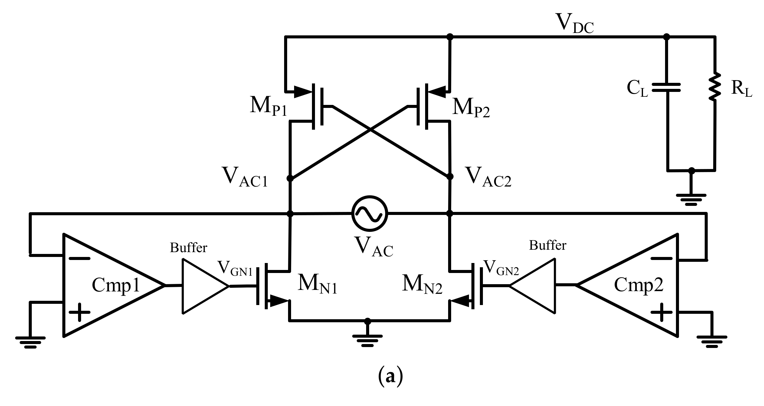
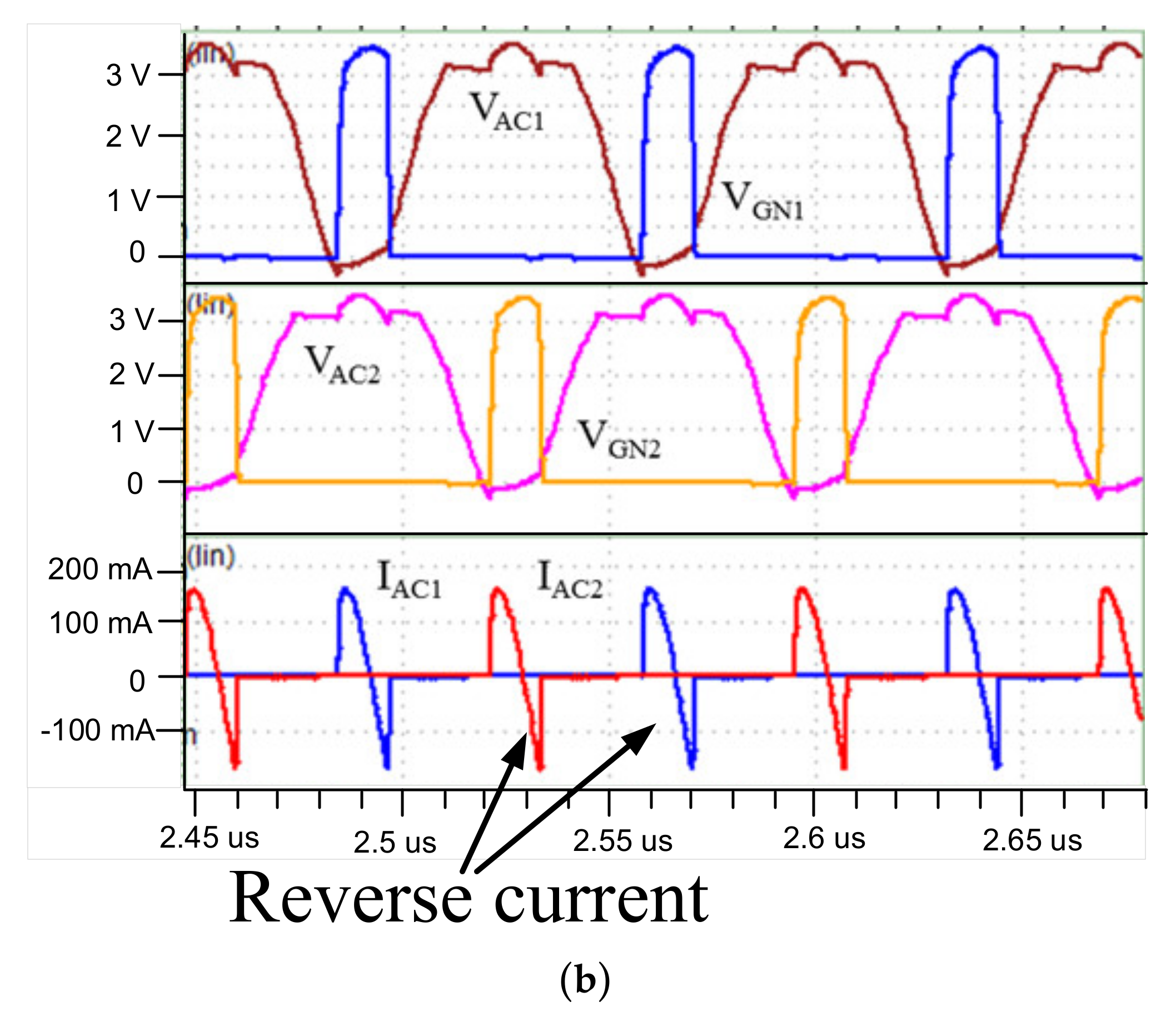
Improving the power conversion efficiency (PCE) of wireless power transmission systems over a wide input voltage range is an important issue. The active rectifier with control pulse (VGN1 and VGN2) is shown in Figure 2a. The active diode (MN1, MN2) adapted on the active rectifier is due to the constant voltage drop of a Schottky diode, which is typically between 0.14 V–0.45V. This device is favored for low-power systems, but for integrated circuits, these require costly fabrication processing and are highly dependent on temperature. The differential fully cross-coupled rectifier has the reverse characteristic of the rectifying devices because the rectifying cross-coupled transistor is still a bidirectional device. The active rectifier always operates at near-optimum conditions with buffer delay elimination to significantly enhance the PCE if the VGN1 and VGN2 signals drive MN1 and MN2 in the incorrect time. The on-and-off propagation delay time of the comparator and buffer causes the power transistor (MN1 and MN2) to turn on and off at incorrect times which will reduce the PCE. For example, in Figure 2b, during the ON propagation delay, this leads to a decrease in the charge time of the rectifier. For the OFF propagation delay, it induces reverse leakage current on the power MOS, as shown in Figure 2b. Figure 2b shows the simulation result of the reverse current. It is crucial to solve the on/off propagation delay problem, even when the delay time varies by input amplitude.
Until now, many kinds of techniques for delay compensation have been proposed [6,7,8,9,10,11,12,13,14,15,16,17,18]. In this work [9], both input signal VAC and ground voltage (VSS) are fed to the error amplifier (EA) for comparison. The error voltage controls the injected current to the push–pull comparator use to compensate the delay. As the feedback loop is stable, it can generate a stable voltage to set the offset current. In Reference [9], the VAC is larger/smaller than VSS, which indicates the NMOS turn off to late/early, and Voffset-off is decreased/increased to allow offset current to turn off NMOS earlier/later. In Reference [10], the feedback-type operational transconductance amplifier (OTA) is replaced with the error amplifier. In this work, it is implemented with a control logic circuit to control the timing of the comparison. The value of VAC is a sample and is passed to the OTA and compared with VSS. The output voltage (Vea_off) of OTA adjusts the offset current of the comparator. After several cycles, Vea_off is adjusted to the steady-state value. For both EA and OTA, it is very slow, and it costs many input cycles to calibrate the correct voltage. In Reference [11], the power stage contains two cross-coupled PMOSs and two power NMOSs (MNA and MNB) controlled by adaptive-delay time control (ADTC) by sensing the input AC signal. The ADTC generates the delayed pulses for power NMOS by tracking the optimal on/off time. The optimal on/off time of the power switches is generated by two current-controlled delay lines (CCDLs) in the ADTC. Therefore, the rising edge and falling control signal of the power NMOS are generated by the delay-line method rather than using the continuous-time comparator. In Reference [13], the control pulse of the power transistor is generated from the digital circuit. The digital circuit is able to control the on/off delay compensated in the active rectifier. The compensation current’s on-current and off-current are injected into the comparators, when they are needed, to reduce the buffer’s delays. A single-comparator architecture and auto-calibration mechanism are implemented in Reference [14]. The falling edge of the gate driving signal should be located at the zero-crossing point of the comparator’s input to prevent reverse current. The auto-calibration mechanism circuit senses the time error in which the output of the comparator is away from the zero-crossing point. In Reference [15], a two-step coarse- and fine-tuning circuit is implemented for shifting the voltage level of the comparator’s input signal. The coarse/fine-tuning block generates digital control signals to adjust the current mirror arrays according to the detection signals. The offset current of the current mirror array could be tuned up or tuned down for a wide delay compensation range. The propagation delay of comparators and buffers is relative to the rail-to-rail supply voltage. In Reference [16], the lower supply rail is provided by the double-pass regulator that shifts the lower supply level from zero voltage to 1.4 V. With this technique, lowering the rail-to-rail supply voltage can improve the delay time of the comparator and buffers. The 3.3 V transistor devices in the comparators and buffers are replaced with 1.8 V devices that can reduce gate capacitance and ON resistance of the transistor. In Reference [17], the dual-loop adaptive delay compensation circuitry for fine control and coarse control isused to adjust the offset of comparator. The initial is set with fine control to provide a smaller level offset current. For fine control, the inputs of the rectifier are sampled and fed to the error amplifier, which generates a DC offset voltage. The offset voltage is proportional to the delay time of the buffer and comparator. The coarse control compares the error voltage with high and low threshold levels for small and large compensation scenarios, respectively.
In this paper, a time-domain technique for compensated delay of the buffer in an active rectifier is proposed to enhance the PCE. The contributions from this paper are highlighted below:
  • The proposed circuit is well-suited for a wide range of input voltage and loading resistors.
  • A phase error detector is proposed to detect the phase difference induced by the buffers. The phase difference is converted to voltage and adaptively tracks the on/off delay time in the rectifier with variable input voltage.
  • This technique can effectively overcome the problem of varied delay time by the buffer in different input voltages.
  • The advantages of our circuits are with high resolution for accuracy-compensated phase difference between input and output buffer. It can generate the desired pulse to turn on/off the power MOS.
The rest of the paper is constructed as follows. The proposed active rectifier circuit is discussed in Section 2. The measurement results are illustrated in Section 3. Section 4 gives the conclusion.

2. Proposed Circuit

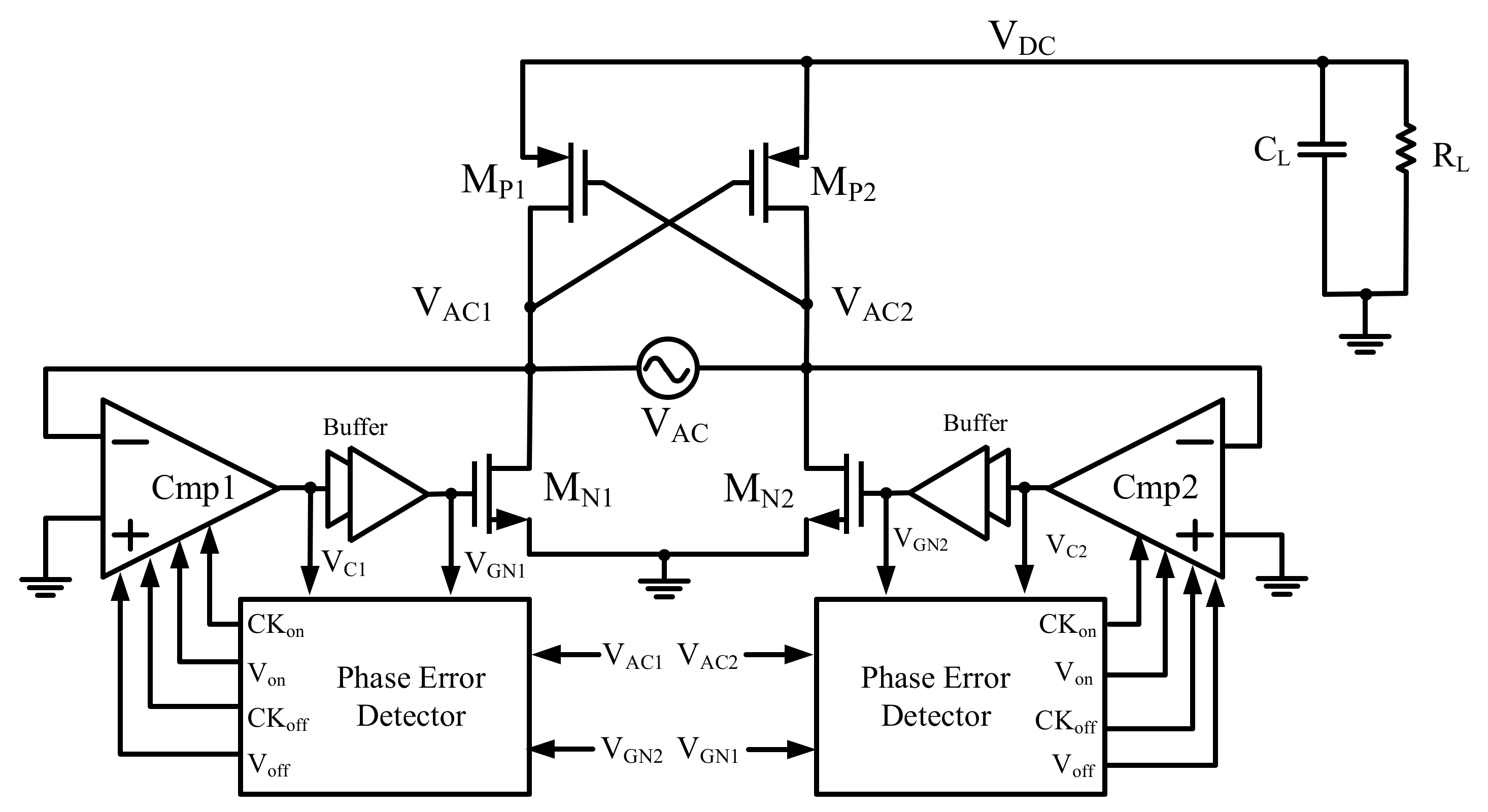
As shown in Figure 3, VAC1 and VAC2 are the input of rectifiers from the receiver coupling inductor VAC. Following the change of VAC1 and VAC2, the four power MOS (MN1, MN2, MP1 and MP2) are controlled. When voltage VAC1 is larger than voltage VAC2, the comparator Cmp2 will generate a high signal to turn on MN2, and the current passes through MP1 to charge the output capacitance CL. During another half cycle, voltage VAC2 is larger than VAC1, the MN2 and MP1 will turn off and the MN1 and MP2 will turn on to continue charging the rectifier output. However, as the comparators’ output passes through the buffer to turn on the power NMOS transistors (MN1, MN2), the buffer will generate a delay time to turn on/off MN1 and MN2. The turn-on delay time to the charge output is less than is required. The turn-off delay time leads to a reverse current problem. These delay problems may waste the power of the rectifier.

2.1. Phase Error Detector

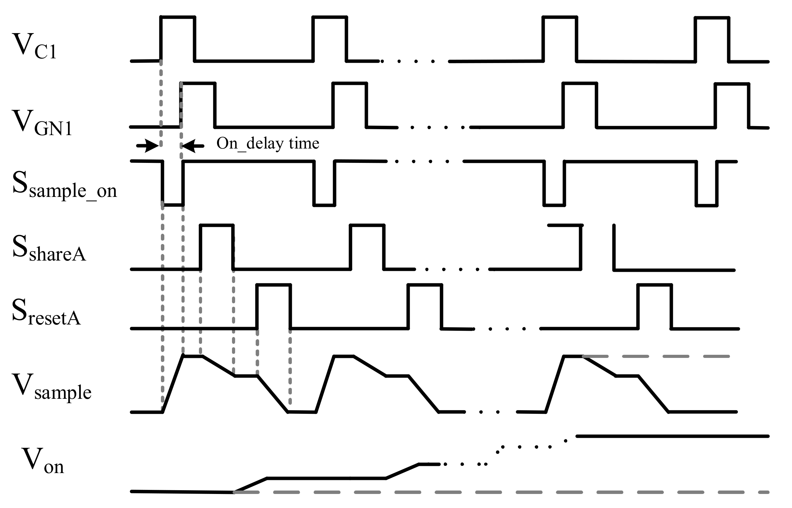
A phase error detector is proposed to detect and compensate the on/off delay time. As shown in Figure 4, the proposed phase error detector consists of logic gates, capacitors and transistors. The phase error detector is able to detect the phase difference between VC1/VC2 and VGN1/VGN2. The phase error is converted into voltage Von and Voff. The operation of the phase detection is described as follows. The proposed circuit detects the phase difference between the VC1 and VGN1 or VC2 and VGN2. The signal Ssample_on is generated by the adjacent rising edge between VC1 and VGN1. The adjacent falling edge between VC1 and VGN1 is the generated signal, Ssample_off. These phase differences are converted by the transistors (M1A, M2A, M3A, M1B, M2B, M3B) and generate two voltages Von and Voff, respectively. The voltages of the Von and Voff depend on pulse width of signal, Ssample_on and Ssample_off. The control signals Ssample_on, Ssample_off, SshareA, SresetA, SshareB and SresetB are generated with logic gates as shown in Figure 4. The timing diagram of the phase error detector is shown in Figure 5. Figure 5 only presents the timing diagram to adjust the on-delay-time of the power MOS. The operation of the generated Von is divided into three steps. The first step, the signal Ssample_on, turns on the M1A and charges the capacitor, C1, for the rising edge difference between input and output the of the buffer. In the second step, the charging sharing between two capacitors, C1 and C2, the voltage Von is charged up. It is controlled by the signal SshareA. In the third step, the voltage of VsampleA is discharged by the signal SresetA to a zero voltage. These steps repeat themselves and generate a stable voltage Von. The off-delay-time is the same operation procedure, but the input signal is the Ssample_off.

2.2. Comparator Circuit

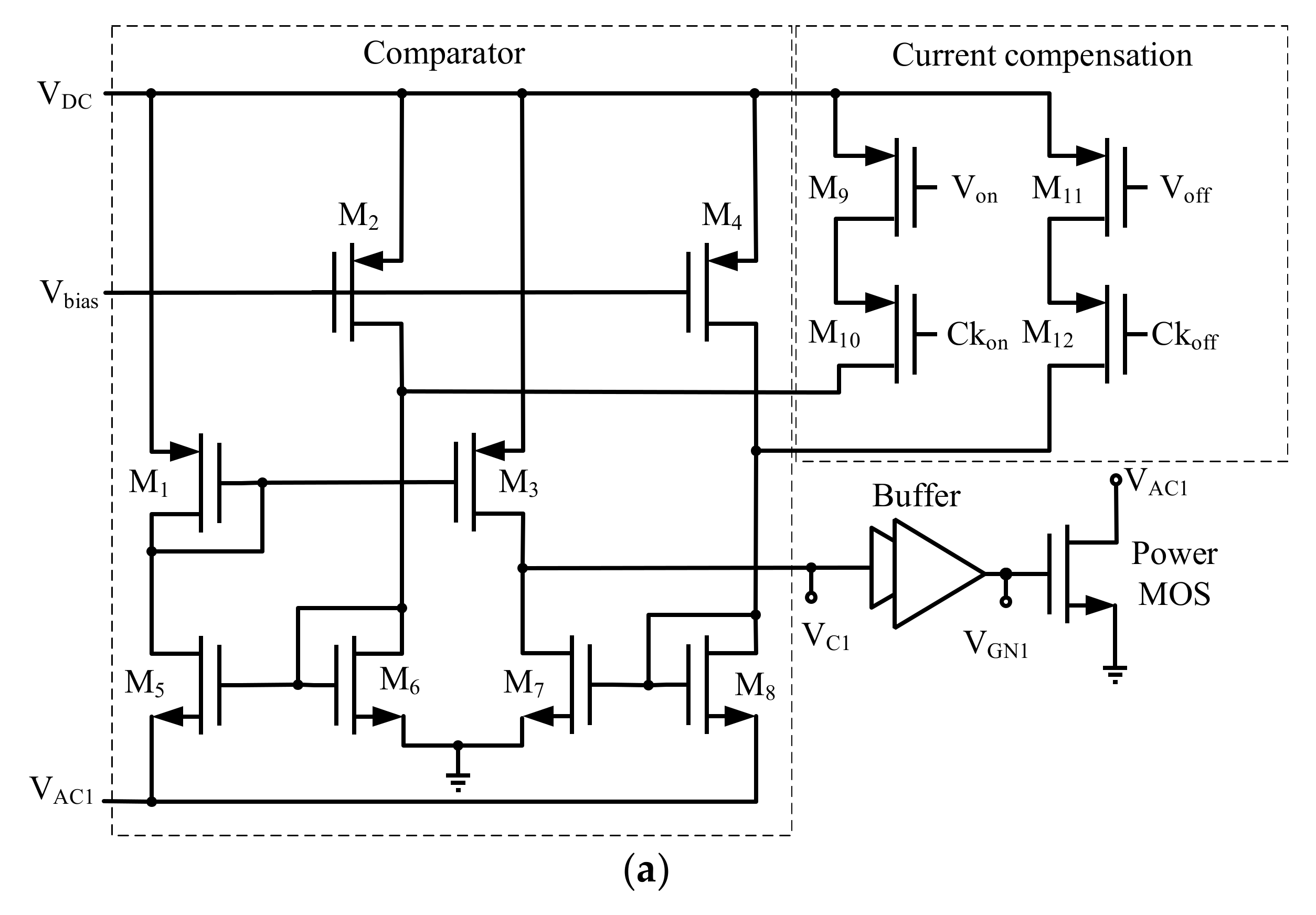
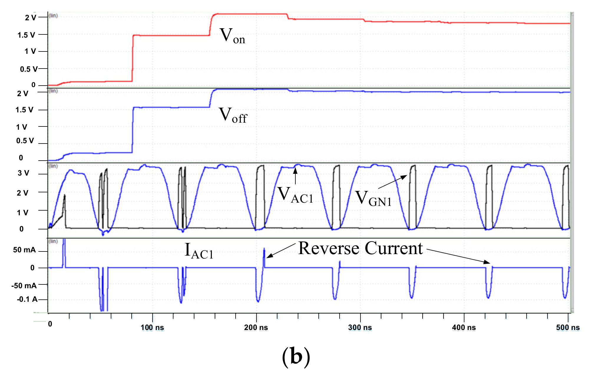
Figure 6a shows the comparator with current compensation transistors. The comparator is implemented with transistors M1–M8. The current compensation circuit is composed of transistors M9–M12. The two clock phases, Ckon and Ckoff, turn on transistors M10 and M12 for injection of the current into the comparator. The Ckon turns on M10 when the VAC1 starts to decrease to 0 V, until VAC1 is lower than 0 V. After Ckon is turned off, Ckoff is turned on M12 until VAC1 becomes a high voltage. The pulse signals Ckon and Ckoff adjust the offset voltage of the comparator. The simulated operation process of the comparator is shown in Figure 6b with a 0.18 μm CMOS process. Figure 6a shows that the simulation waveform of the proposed phase error detector generates two stable voltages, Von and Voff. These voltages give the comparators with adaptive offset the voltage to solve the delay due to the buffer. In Figure 6b, the edge of VGN1 is turned on earlier in each cycle, and the reverse current IAC1 gradually decreases.

2.3. PCE Analysis and Considerations

The power conversion efficiency (PCE) is one of the important parameters in the full-wave rectifier. A simplified equivalent circuit model of an active full-wave rectifier is shown in Figure 7. The AC power supply, VAC, represents the AC power from the secondary LC-resonant coil. The switches represent the power NMOS transistors (MN1, MN2). The capacitors, Cg,p, represent the equivalent capacitance on the power PMOS transistors. The resistors, RS, represent the turn-on resistance of both p-type and n-type power transistors. The output load, RL and CL, represents the output resistance and output capacitance load, respectively. To estimate the PCE, the charge and discharge equation is given by Equations (1) and (2).
Q c h = C L × Δ V = I R S I R L × 2 × D × T S
Q d i s = C L × Δ V = I R L × 1 2 D × T S
where D is the duty cycle, and TS is the period of the resonant frequency.
The proposed rectifier comprises symmetrical circuits, the charge and discharge are equal and the current flows from RS and RL can be described as follows.
Q c h = Q d i s I R S = 1 2 D I R L = 1 2 D V D C R L
By calculating the current equation, the power dissipation on the proposed rectifier can be estimated as follows (Equation (4)):
P C E = P L o a d P L o a d + 2 × P r o n , p + P r o n , n + P s w p , c g + P c o m p
In Equation (4), the PLoad represents the output power on the RL and CL, and the PLoad is calculated according to Equation (5):
P L o a d = V D C 2 R L
Because of the full-wave structure, the switching and turn power dissipation would happen twice in a period once switching and turn power dissipation are doubled. The Pron,p and Pron,n represent the turn-on power NMOS transistors (MN1, MN2) and power PMOS transistors (MP1, MP2), respectively, and the summation of Pron,p and Pron,n can also be considered as the power consumption on the RS shown in Figure 7. The power consumption of the turn-on resistance can be calculated as
P r o n , p = I R S 2 × D × R o n , p = 1 2 D V D C R L 2 × D × R o n , p = 1 4 D V D C R L 2 × R o n , p
P r o n , n = 1 4 D V D C R L 2 × R o n , n
where IRS can be substituted by Equation (3). In Equations (6) and (7), the Ron,p and Ron.n represent the linear resistance of the power transistors. This resistance can be described as Equation (8).
R o n = 1 μ C o x W L V G S V T H
The switching power Pswp,cg includes the buffer and the comparator in the proposed rectifier. The switching power Pswp,cg has a switching frequency fs and creates a path for current to charge or discharge the capacitance on the power transistors Cg,p. The switching power can be described by Equation (9). The power consumption of the comparator is eliminated.
P s w p , c g = C g , p × V D C 2 × f s
Figure 8 shows the power consumption pie chart of the post-simulation result. This result is simulated under the output load, 300 Ω, and the input VDC is 3.3 V, which is the highest PCE situation. This simulation includes the parasitic capacitance in the layout, so the power consumption of the inverters is closer to the real chip. The 0.18 μm process includes 1.8 V/3.3 V dual-voltage devices. The proposed circuit is realized with only 3.3 V NMOS/PMOS devices. The breakdown voltage of 3.3 V and 0.18 μm CMOS technology is around 4 V. Therefore, the transistor works at less than 4 V to prevent damage to the transistor. The simulation result of the voltage conversion ratio (VCR) and PCE under the different process corner TT, FF and SS, is shown in Figure 9 and Figure 10. The simulated VCR with the input voltage that ranges from 2 V to 3.6 V with RLoad = 300 Ω, as shown in Figure 9. This result verifies that the VCR of the proposed rectifier has the worst VCR, 88.7%, for SS corner. Figure 10 shows the simulated result of PCE of proposed rectifier versus output load RLoad under different process corners TT, FF and SS, when the AC input peak–peak amplitude is fixed at 3.6 V. The simulated PCE result has a slight drop of around 1% to 6%, especially in heavy loads for the SS corner. The simulation of the variation with the process and temperature is included in Table 1. This result shows that the proposed active rectifier has a very stable PCE with 3.9% of variation and VCR with 2% of variation under different processes and temperatures.

3. Measurement Results

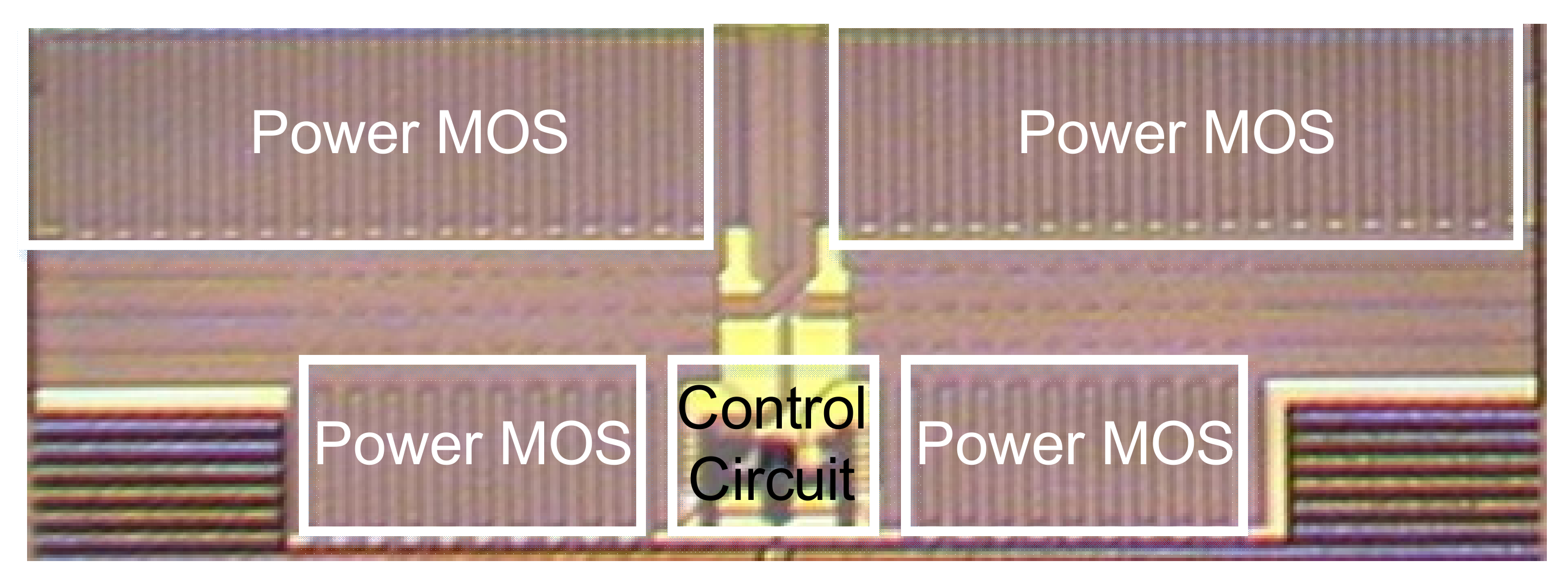
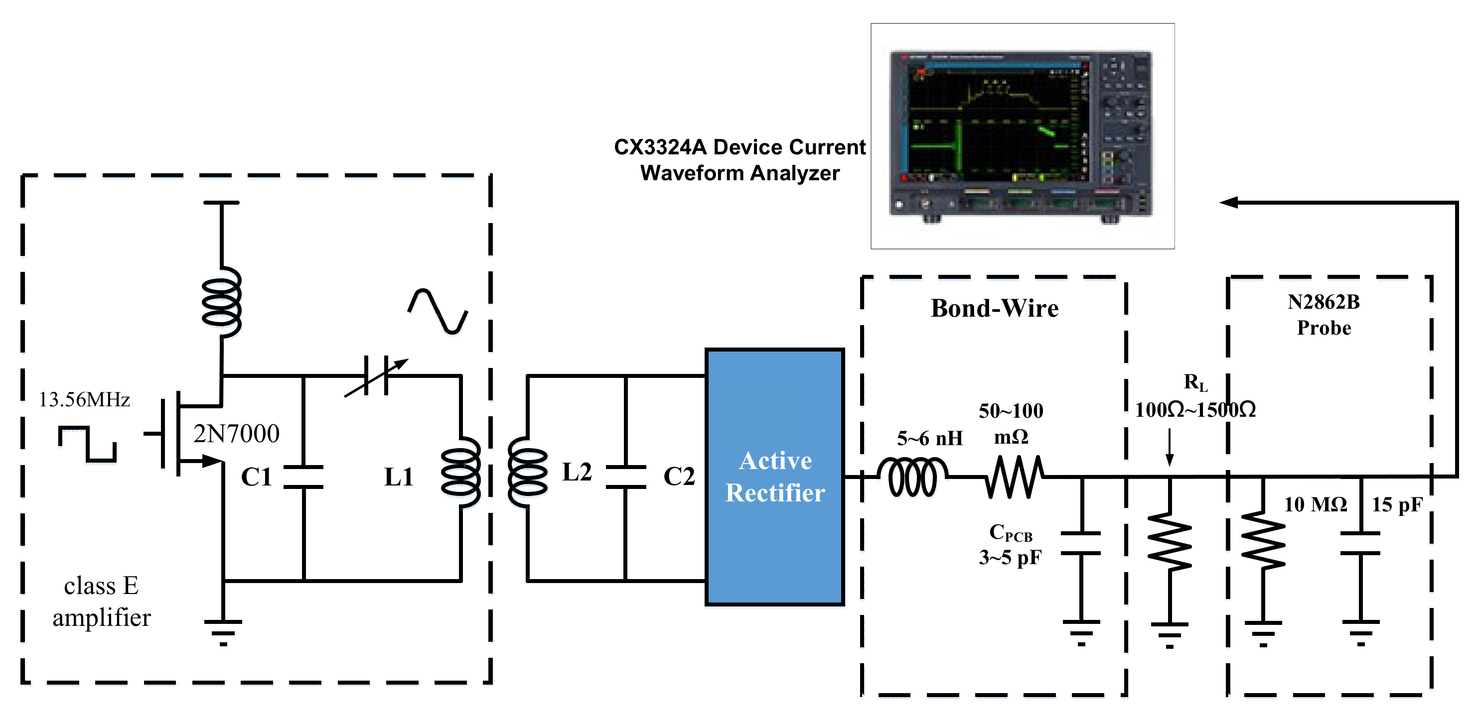
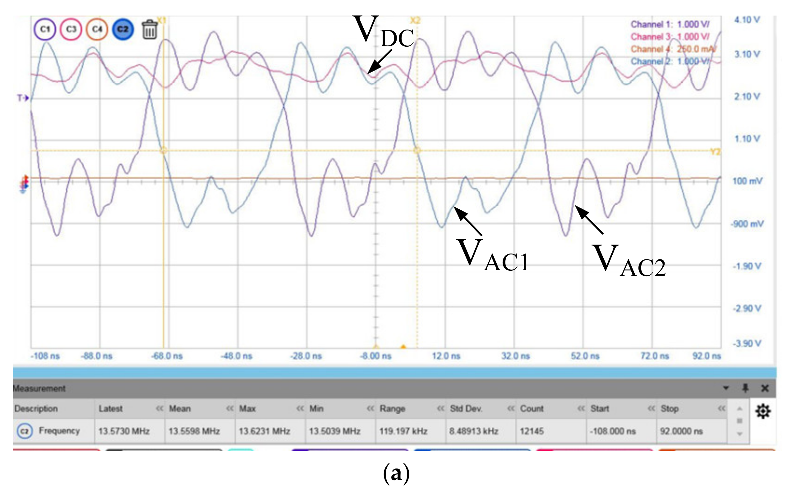
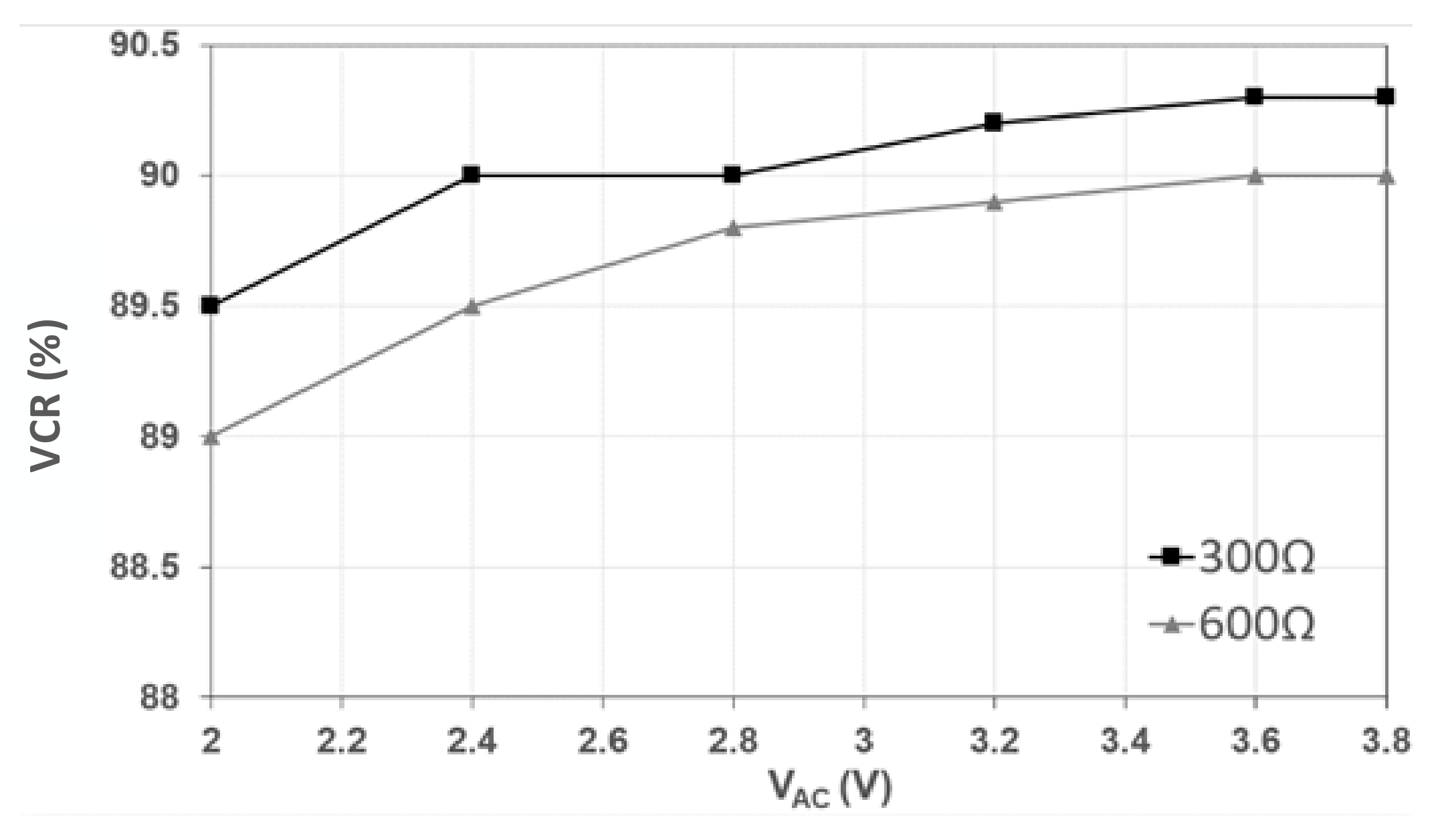
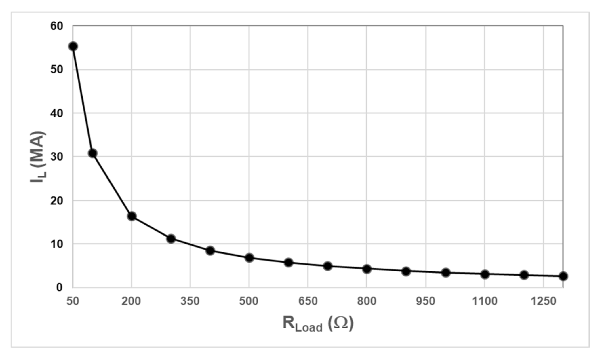
The proposed rectifier is fabricated in 0.18 μm CMOS process with standard I/O devices. The microphotograph with its floorplan is shown in Figure 11. The core area of the chip is 0.24 mm2. The outputs of the active rectifier included in the external resister and capacitor are 300 Ω and 2 nF, respectively. The measurement setup is shown in Figure 12. The experimental setup includes a current waveform analyzer Keysight CX3324A, CX1101A current probe and N2862B passive probe (Keysight Technologies, Santa Rosa, CA, USA). In this measurement, the distance between primary coil L1 and secondary coil L2 would influence the magnetic resonant amplitude. Therefore, we put it as close as possible for maximum amplitude to be received by the inductor L2. The proposed IC die is attached directly to PCB and bonded out with 5–6 mm aluminum wire. The ringing of the measured signal is due to the bond wire and the onboard capacitance in the PCB. The AC input voltage amplitude ranges from 2 V to 3.8 V, and the resonant frequency is fixed at 13.56 MHz. Figure 13a shows the measured waveform of the active rectifier without a phase error detector. Figure 13a shows very serious ringing for the AC input waveforms, and the ringing inside the chip is expected to be even more serious. Figure 13b shows the measured waveform of the active rectifier without the phase error detector. Figure 13b shows less ringing for the AC input waveform and demonstrates the effectiveness and accuracy of the proposed technique. Figure 14 shows the measured PCEs with load resistor that range from 100 Ω to 1300 Ω when the input voltage is 3.3 V. As shown in Figure 14, the minimum load resistance is 50 Ω with 2 nF of the external capacitor. The optimized PCE is allocated at 300 Ω load, and its output power is 109 mW. Figure 15 shows the performance of the rectifier in various input voltages. The measured VCR with the output voltage ranging from 2 V to 3.8 V are higher than 90.3% when RLoad = 300 Ω and 90% when RLoad = 600 Ω, respectively. The measured result of the output current with output load resistance ranging from 100 Ω to 1300 Ω is shown in Figure 16. The proposed rectifier generates current from 2.6 mA up to 55.4 mA with 3.3 V input voltage. Table 2 compares the performance of the proposed work with state-of-the-art active rectifiers. The proposed rectifier achieves high PCE and VCE over a wide loading range from 100 Ω to 1.3 kΩ. A peak PCE of 90.3% and maximum output power of 109 mW are achieved at 3.3V input voltage. The proposed circuit is well-suited for a wide range of input voltage and loading resistors. The phase error detector works well to remove the phase difference due to the buffer itself.

4. Conclusions

In this paper, an active rectifier with a phase error detector is presented to compensate the phase difference due to the buffer in the rectifier. The rectifier has a high power efficiency over a wide input range from 2 V to 3.8 V. A peak PCE of 90.3% and maximum output power of 109 mW are achieved at 3.3 V input voltage.

Funding

This work was supported by the Ministry of Science and Technology, Taiwan, under Grant MOST 109-2221-E-182-053.

Acknowledgments

The research was supported by the Ministry of Science and Technology, Taiwan, under Grant MOST 109-2221-E-182-053. The authors would like to thank the EDA tool supports and the chip manufacturer of Taiwan Semiconductor Research Institute (TSRI).

Conflicts of Interest

The author declares no conflict of interest.

References

  1. Campi, T.; Cruciani, S.; Palandrani, F.; De Santis, V.; Hirata, A.; Feliziani, M. Wireless Power Transfer Charging System for AIMDs and Pacemakers. IEEE Trans. Microw. Theory Tech. 2016, 64, 633–642. [Google Scholar] [CrossRef]
  2. Akin, T.; Najafi, K.; Bradley, R.M. A wireless implantable multichannel digital neural recording system for a microm-achined sieve electrode. IEEE J. Solid State Circuits 1998, 33, 109–118. [Google Scholar] [CrossRef] [Green Version]
  3. Bhatti, P.T.; Wise, K.D. A 32-Site 4-Channel High-Density Electrode Array for a Cochlear Prosthesis. IEEE J. Solid State Circuits 2006, 41, 2965–2973. [Google Scholar] [CrossRef]
  4. Rothermel, A.; Liu, L.; Pour Aryan, N.; Fischer, M.; Wuenschmann, J.; Kibbel, S.; Harscher, A. A CMOS Chip with Active Pixel Array and Specific Test Features for Subretinal Implantation. IEEE J. Solid State Circuits 2008, 44, 290–300. [Google Scholar] [CrossRef]
  5. Rana, M.M.; Xiang, W.; Wang, E.; Li, X.; Choi, B.J. Internet of Things Infrastructure for Wireless Power Transfer Systems. IEEE Access 2018, 6, 19295–19303. [Google Scholar] [CrossRef]
  6. Kao, S. An Active Rectifier with Time-Domain Delay Compensation to Enhance the Power Conversion Efficiency. World Academy of Science, Engineering and Technology. Int. J. Energy Power Eng. 2019, 13, 168–173. [Google Scholar]
  7. Lu, Y.; Ki, W. A 13.56 MHz CMOS Active Rectifier with Switched-Offset and Compensated Biasing for Biomedical Wireless Power Transfer Systems. IEEE Trans. Biomed. Circuits Syst. 2014, 8. [Google Scholar] [CrossRef] [PubMed]
  8. Li, X.; Tsui, C.-Y.; Ki, W.-H. A 13.56 MHz Wireless Power Transfer System with Reconfigurable Resonant Regulating Rectifier and Wireless Power Control for Implantable Medical Devices. IEEE J. Solid State Circuits 2015, 50, 978–989. [Google Scholar] [CrossRef]
  9. Huang, C.; Kawajiri, T.; Ishikuro, H. A Near-Optimum 13.56 MHz CMOS Active Rectifier with Circuit-Delay Real-Time Calibrations for High-Current Biomedical Implants. IEEE J. Solid State Circuits 2016, 51, 1797–1809. [Google Scholar] [CrossRef]
  10. Cheng, L.; Ki, W.; Lu, Y.; Yim, T. Adaptive On/Off Delay-Compensated Active Rectifiers for Wireless Power Transfer Systems. IEEE J. Solid State Circuits 2016, 51, 712–723. [Google Scholar]
  11. Xue, Z.; Fan, S.; Li, D.; Zhang, L.; Gou, W.; Geng, L. A 13.56 MHz, 94.1% Peak Efficiency CMOS Active Rectifier with Adaptive Delay Time Control for Wireless Power Transmission Systems. IEEE J. Solid State Circuits 2019, 54, 1744–1754. [Google Scholar] [CrossRef]
  12. Fuh, J.; Hsieh, S.-K.; Yang, F.-B.; Chen, P.-H. A 13.56MHz power-efficient active rectifier with digital offset compensation for implantable medical devices. In Proceedings of the 2016 IEEE Wireless Power Transfer Conference (WPTC); Institute of Electrical and Electronics Engineers (IEEE): New York, NY, USA, 2016; pp. 1–3. [Google Scholar]
  13. Cheng, L.; Ge, X.; Hu, L.; Yao, Y.; Ki, W.-H.; Tsui, C.-Y. A 40.68-MHz Active Rectifier with Hybrid Adaptive On/Off Delay-Compensation Scheme for Biomedical Implantable Devices. IEEE Trans. Circuits Syst. I Regul. Pap. 2019, 67, 516–525. [Google Scholar] [CrossRef]
  14. Li, C.-A.; Lee, W.-E.; Lu, C.-H.; Lin, S.-Y.; Lin, T.-H. A Single-Comparator Active Rectifier with Auto-Calibration in 0.18-μm CMOS. In Proceedings of the 2020 IEEE International Symposium on Circuits and Systems (ISCAS); Institute of Electrical and Electronics Engineers (IEEE): New York, NY, USA, 2020; pp. 1–4. [Google Scholar]
  15. Ma, Y.; Cui, K.; Ye, Z.; Sun, Y.; Fan, X. A 13.56-MHz Active Rectifier with SAR-Assisted Coarse-Fine Adaptive Digital Delay Compensation for Biomedical Implantable Devices. IEEE Solid State Circuits Lett. 2020, 3, 122–125. [Google Scholar] [CrossRef]
  16. Rashidi, A.; Laursen, K.; Hosseini, S.; Huynh, H.; Moradi, F. An Implantable Ultrasonically Powered System for Optoge-netic Stimulation with Power-Efficient Active Rectifier and Charge-Reuse Capability. IEEE Tran. Biomed. Circuits Syst. 2019, 13, 1362–1371. [Google Scholar] [CrossRef]
  17. Erfani, R.; Marefat, F.; Mohseni, P. A 1–10MHz Frequency-Aware CMOS Active Rectifier with Dual-Loop Adaptive Delay Compensation and >230 mW Output Power for Capacitively Powered Biomedical Implants. In Proceedings of the 2019 IEEE Custom Integrated Circuits Conference (CICC); Institute of Electrical and Electronics Engineers (IEEE): New York, NY, USA, 2019; pp. 1–4. [Google Scholar]
  18. Cha, H.-K.; Park, W.-T.; Je, M. A CMOS Rectifier with a Cross-Coupled Latched Comparator for Wireless Power Transfer in Biomedical Applications. IEEE Trans. Circuits Syst. II Express Briefs 2012, 59, 409–413. [Google Scholar] [CrossRef]
Figure 1. Wireless power transfer system.
Electronics 10 01450 g001
Figure 2. (a) Active rectifier without delay calibration circuit, (b) reverse current problem.
Electronics 10 01450 g002aElectronics 10 01450 g002b
Figure 3. Active rectifier with phase error detector.
Electronics 10 01450 g003
Figure 4. Phase error detector.
Electronics 10 01450 g004
Figure 5. Timing diagram of phase error detector.
Electronics 10 01450 g005
Figure 6. (a) Comparator circuit, (b) simulation result of Von and Voff.
Electronics 10 01450 g006aElectronics 10 01450 g006b
Figure 7. Equivalent circuit model of an active full-wave rectifier.
Electronics 10 01450 g007
Figure 8. Pie chart of power consumption.
Electronics 10 01450 g008
Figure 9. Voltage conversion ratio (VCR) versus different input voltage.
Electronics 10 01450 g009
Figure 10. Power conversion efficiency (PCE) versus different output load.
Electronics 10 01450 g010
Figure 11. Microphotograph of the proposed circuit.
Electronics 10 01450 g011
Figure 12. Measurement setup.
Electronics 10 01450 g012
Figure 13. Measured waveforms of the proposed rectifier (a) without phase error detector and (b) with phase error detector.
Electronics 10 01450 g013aElectronics 10 01450 g013b
Figure 14. Measured PCE under different load resistors.
Electronics 10 01450 g014
Figure 15. Measured VCR under different input voltage.
Electronics 10 01450 g015
Figure 16. Output current versus different output loads.
Electronics 10 01450 g016
Table 1. Power conversion efficiency (PCE) and voltage conversion ratio (VCR) versus process and temperature.
Simulation Result
CornerTemperature (°C)PCE (%)VCR (%)
TT2792.5%92.5%
SS10088.7%90.6%
FF092.6%92.6%
Table 2. Comparison with prior works.
Parameters[18]
TCASII’12
[9]
JSSC’16
[11]
JSSC’19
This Work
Technology (μm)0.180.180.180.18
Frequency (MHz)13.5613.5613.5613.56
Input Amp.(V)0.9–21.3–2.51.0–2.51.8–3.6
Output Amp.(V)0.45–1.781.24–2.440.928–2.371.62–3.35
Pout (Max. mW)3.2248.134.1109
VCR (%)82–89
( R L o a d = 1   k Ω )
91.7–95.2
( R L o a d = 100   Ω )
92.8–97.5
( R L o a d = 510   Ω )
89–90.3
( R L o a d = 200   Ω )
PCE (%)60–81.9
( R L o a d = 1   k Ω )
91.3–94.6
( R L o a d = 100   Ω 500   Ω )
82.6–94.1
( R L o a d = 510   Ω 2   k Ω )
83–90.3
( R L o a d = 100   Ω 1.3   k Ω )
Publisher’s Note: MDPI stays neutral with regard to jurisdictional claims in published maps and institutional affiliations.