
An Ultra-Wideband Compact TR Module Based on 3-D Packaging


Abstract
1. Introduction
2. General Aspects and Requirements
2.1. Overview of the TR Module Design
2.2. Electrical Specification
3. Module Design
3.1. Circuit Schematic Design
- Digitally controlled multi-functional MMICs made in GaAs for amplitude/phase conditioning of transmitting and receiving signal. Nominal Tx gain: 11 dB. Nominal Rx gain: 6 dB.
- HPA (GaN) with power switch (GaN) multi-functional MMICs. Saturation output power: 33 dBm. Power Gain: 10 dB.
- DPA (GaAs) with power-switch multi-functional MMICs. Saturation output power: 26 dBm. Power gain: 13 dB.
- LNA (GaAs) with limiter multi-functional MMICs. Nominal gain: 21dB. Nominal NF: 1.5 dB. Limit power: 2 W.
3.2. Circuit Layout and Mechanical Design
3.3. Thermal Design
4. Key Schematic Design and Circuit Simulation
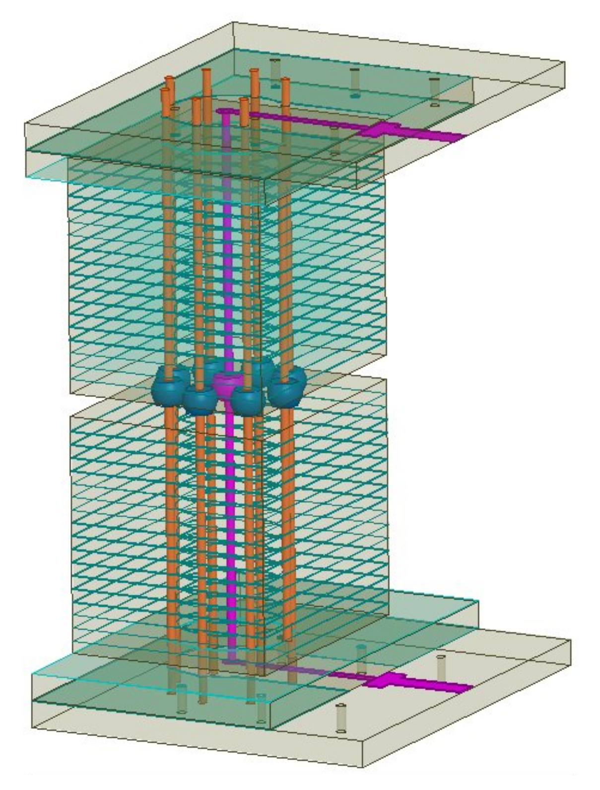
4.1. BGA Ball Vertical Interconnection
4.2. SSMP Vertical Interconnection
5. Module Assembling and Testing
6. Conclusions
Author Contributions
Funding
Institutional Review Board Statement
Informed Consent Statement
Conflicts of Interest
References
- Matevosyan, H.; Poghosyan, A.; Golkar, A. A value-chain analysis for the copernicus earth observation infrastructure evolution: A knowledgebase of users, needs, services, and products. IEEE Geosci. Remote Sens. Mag. 2017, 5, 19–35. [Google Scholar] [CrossRef]
- Bartocci, M.; de Santis, G.; Giolo, G.; Rossi, L.; Gemma, M. 4W TX/RX Multi Chip Module for 6-18GHz Phased Array. In Gallium Arsenide Applications Symposium, GAAS; Alma Mater Studiorum-University of Bologna: Bologna, Italy, 2001. [Google Scholar]
- Alarcón, E.; Sanchez, A.A.; Araguz, C.; Barrot, G.; Bou-Balust, E.; Camps, A.; Cornara, S.; Cote, J.; Peña, A.G.; Lancheros, E.; et al. Design and optimization of a polar satellite mission to complement the copernicus system. IEEE Access 2018, 6, 34777–34789. [Google Scholar] [CrossRef]
- Lacomme, P. New trends in airborne phased array radars. IEEE Int. Symp. 2003, 17–22. [Google Scholar] [CrossRef]
- Ma, J.; Sun, W.; Yang, G.; Zhang, D. Hydrological analysis using satellite remote sensing big data and CREST model. IEEE Access 2018, 6, 9006–9016. [Google Scholar] [CrossRef]
- Baccello, D.; D’Antoni, M.; Orobello, B.; Sperduti, E. Miniaturised low cost solid state 4W TXRX common leg for 6–18 GHz phased array. IEEE MTT-S Int. 2010, 1. [Google Scholar] [CrossRef]
- Bian, X.; Shao, Y.; Wang, S.; Tian, W.; Zhang, C. Shallow water depth retrieval from multitemporal sentinel-1 SAR data. IEEE J. Sel. Top. Appl. Earth Obs. Remote Sens. 2018, 11, 2991–3000. [Google Scholar] [CrossRef]
- Schuh, P.; Sledzik, H.; Reber, R.; Fleckenstein, A.; Leberer, R.; Oppermann, M.; Quay, R.; Van Raay, F.; Seelmann-Eggebert, M.; Kiefer, R.; et al. GaN MMIC based T/R-Module Front-End for X-Band Applications. In Proceedings of the 2008 European Microwave Integrated Circuit Conference, Amsterdam, The Netherlands, 27–28 October 2008; pp. 274–277. [Google Scholar] [CrossRef]
- Joerg, H.; Pardini, M.; Hajnsek, I.; Papathanassiou, K.P. Sensitivity of SAR tomography to the phenological cycle of agricultural crops at X-, C-, and L-band. IEEE J. Sel. Top. Appl. Earth Obs. Remote Sens. 2018, 11, 3014–3029. [Google Scholar] [CrossRef]
- Savidis, I.; Friedman, E.G. Closed-form expressions of 3-D via resistance, inductance, and capacitance. IEEE Trans. Electron Devices 2009, 56, 1873–1881. [Google Scholar] [CrossRef]
- Le, B.T.; Xiao, D.; Mao, Y.; He, D.; Zhang, S.; Sun, X.; Liu, X. Coal exploration based on a multilayer extreme learning machine and satellite images. IEEE Access 2018, 6, 44328–44339. [Google Scholar] [CrossRef]
- Colangeli, S.; Bentini, A.; Ciccognani, W.; Limiti, E.; Nanni, A. GaN-Based Robust Low-Noise Amplifiers. IEEE Trans. Electron Devices 2013, 60, 3238–3248. [Google Scholar] [CrossRef]
- Xu, W.; Deng, Y.; Wang, R. Multichannel synthetic aperture radar systems with a planar antenna for future spaceborne microwave remote sensing. IEEE Aerosp. Electron. Syst. Mag. 2012, 27, 26–30. [Google Scholar] [CrossRef]
- Rieger, R.; Schweizer, B.; Dreher, H.; Reber, R.; Adolph, M.; Feldle, H.-P. Highly integrated cost-effective standard X-band T/R module using LTCC housing concept for automated production. In Proceedings of the IEEE Colloquium on ‘Synthetic Aperture Radar Digest’, London, UK, 29 November 2002; pp. 303–306. [Google Scholar]
- Golkar, A.; Cruz, I.L. The federated satellite systems paradigm: Concept and business case evaluation. Acta Astron. 2015, 111, 230–248. [Google Scholar] [CrossRef]
- Yu, Z.; Xu, Z.; Deng, Y.; Zhang, Z. An Overall LTCC package solution for X-band tile T/R module. Electromagn. Res. Lett. 2013, 38, 181–192. [Google Scholar] [CrossRef]


| Parameter | Measured Data |
|---|---|
| Frequency Range | 2~12 GHz |
| Rx Gain | 15~18 dB |
| Noise Figure | 4.2~5.5 dB |
| Rx Input P−1 | ≥−20 dBm |
| Maximum Tx Gain | 30 dB |
| Tx Output Power | 32~34.5 dBm (CW) |
| VSWR | <1.8 |
| Phase Variation Range | 0~720° (6-bit) |
| RMS Phase Error | <6° |
| Attenuation Range | 0~31.5 dB (6-bit) |
| RMS Attenuation Error | <0.5 dB |
| Tx Harmonic Suppression | ≤−15 dBc (in band), ≤−25 dBc (out of band) |
| Switch Time (T/R) | <500 ns |
| System Bias | +5 V, +28 V, −40 V, −5 V |
| Package Technology | 3-D multilayer package with BGA balls |
| Module Type | Blade | Tile Type | 3-D Tile Type |
|---|---|---|---|
| Physical Photo |  |  |  |
| Operating Band | 6–18 GHz | 2–6 GHz | 2–12 GHz |
| Number of Channels | 4 | 4 | 4 |
| Dimensions | 80 × 37.5 × 10 mm3 | 49.8 × 49.8 × 13.5 mm3 | 27.8 × 27.8 × 12 mm3 |
| Weight | 60 g | 70 g | 25 g |
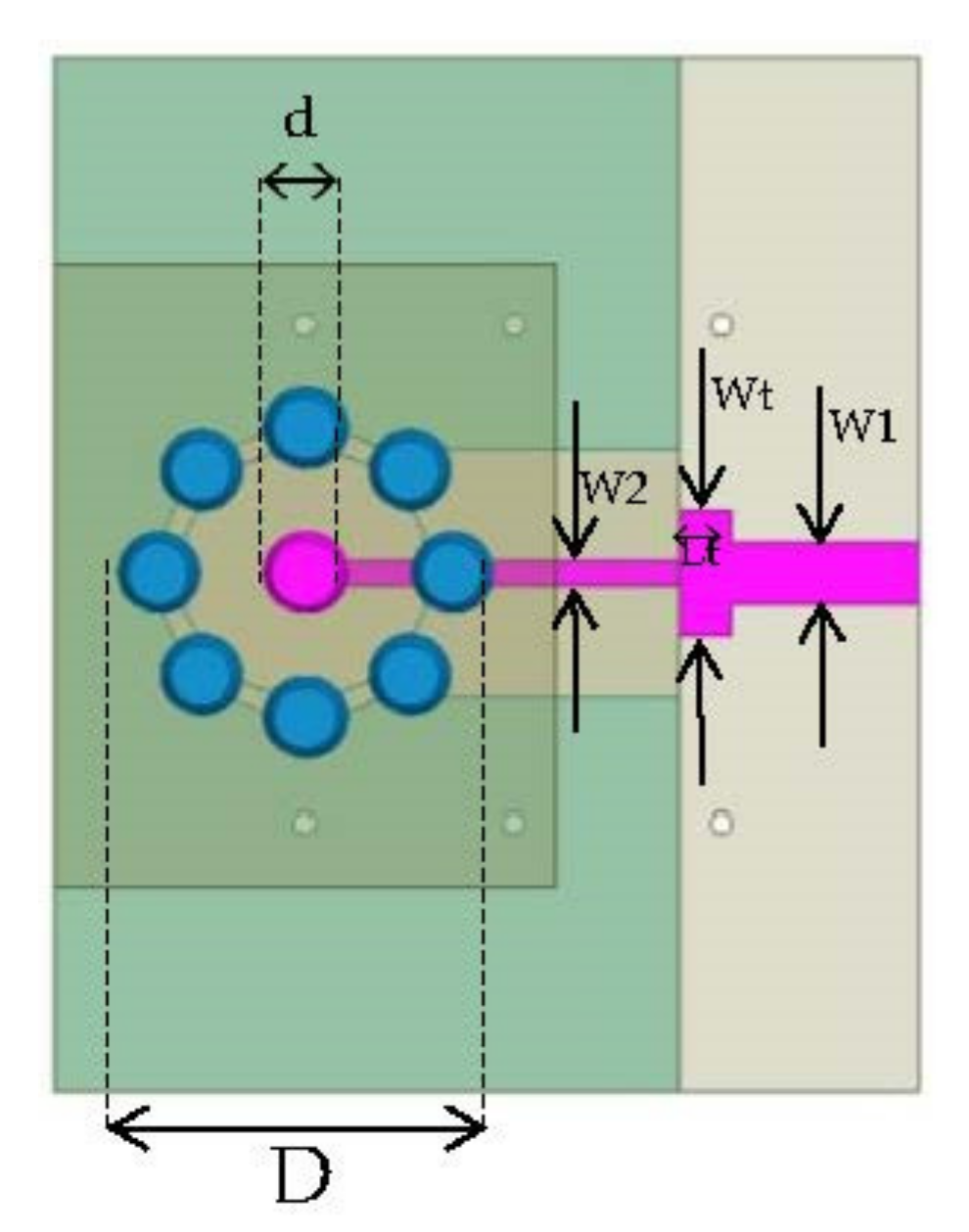
| Parameter Name | D | d | W1 | W2 | Wt | Lt |
|---|---|---|---|---|---|---|
| Value (mm) | 1.1 | 0.4 | 0.3 | 0.12 | 0.42 | 0.2 |
Publisher’s Note: MDPI stays neutral with regard to jurisdictional claims in published maps and institutional affiliations. |
© 2021 by the authors. Licensee MDPI, Basel, Switzerland. This article is an open access article distributed under the terms and conditions of the Creative Commons Attribution (CC BY) license (https://creativecommons.org/licenses/by/4.0/).
Share and Cite
Li, Z.; Sun, H.; Wu, H.; Zhang, S. An Ultra-Wideband Compact TR Module Based on 3-D Packaging. Electronics 2021, 10, 1435. https://doi.org/10.3390/electronics10121435
Li Z, Sun H, Wu H, Zhang S. An Ultra-Wideband Compact TR Module Based on 3-D Packaging. Electronics. 2021; 10(12):1435. https://doi.org/10.3390/electronics10121435
Chicago/Turabian StyleLi, Zhiqiang, Houjun Sun, Hongjiang Wu, and Shuai Zhang. 2021. "An Ultra-Wideband Compact TR Module Based on 3-D Packaging" Electronics 10, no. 12: 1435. https://doi.org/10.3390/electronics10121435
APA StyleLi, Z., Sun, H., Wu, H., & Zhang, S. (2021). An Ultra-Wideband Compact TR Module Based on 3-D Packaging. Electronics, 10(12), 1435. https://doi.org/10.3390/electronics10121435