Review

A Review on Improved Design Techniques for High Performance Planar Waveguide Slot Arrays

by
Giovanni Andrea Casula
*,
Giuseppe Mazzarella
,
Giorgio Montisci
and
Giacomo Muntoni
Dipartimento di Ingegneria Elettrica ed Elettronica, Università degli Studi di Cagliari, 09123 Cagliari, Italy
*
Author to whom correspondence should be addressed.
Electronics 2021, 10(11), 1311; https://doi.org/10.3390/electronics10111311
Submission received: 26 April 2021 / Revised: 24 May 2021 / Accepted: 27 May 2021 / Published: 30 May 2021
(This article belongs to the Special Issue RF/Microwave Circuits for 5G and Beyond)

Abstract

:
Planar waveguide slot arrays (WSAs) have been used since 1940 and are currently used as performing antennas for high frequencies, especially in applications such as communication and RADAR systems. We present in this work a review of the most typical waveguide slot array configurations proposed in the literature, describing their main limitations and drawbacks along with possible effective countermeasures. Our attention has been focused mainly on the improved available design techniques to obtain high performance WSAs. In particular, the addressed topics have been reported in the following. Partially filled WSAs, or WSAs covered with single or multilayer dielectric slabs, are discussed. The most prominent second-order effects in the planar array feeding network are introduced and accurately modeled. The attention is focused on the T-junction feeding the array, on the effect of interaction between each slot coupler of the feeding network and the radiating slots nearest to this coupler, and on the waveguide bends. All these effects can critically increase the first sidelobes if compared to the ideal case, causing a sensible worsening in the performance of the array.

1. Introduction

Waveguide slot arrays and antennas (WSAs) are made of slots cut in the wall of a guided structure, which behaves as a set of antennas. The first employment of these peculiar radiating structures can be dated back to the 1940s [1], but the intrinsic advantages of the antennas (e.g., feed and radiating element integrated in the same structure, low insertion loss, tunable radiation pattern, low cross-polarization levels, and ease of fabrication) granted them a long-lasting popularity which has endured to this day. Indeed, they are currently used as performing antennas for high frequencies, mainly in applications such as communication and RADAR systems, as well as for aerospace and satellite applications [2].
In many applications, especially for frequencies beyond the X band, WSAs are a better choice compared with both reflector and printed antennas, especially because they are characterized by high radiation efficiency, high mechanical strength, the capability of handling high power, and low losses [2,3]. On the other hand, being WSA resonant antennas, they have a relatively narrow bandwidth, a high cost of production, and are not easily reconfigurable because once the array has been realized, it is hard to change its electromagnetic behavior [4]. The pros and cons of WSAs are summarized in Table 1.
The listed features make WSAs suitable for RADAR and remote sensing applications within a frequency range starting from the higher part of the S band to millimeter waves and above. In fact, the typical requirements for such antennas are the capability of handling high power and low losses, together with a relatively narrow bandwidth, and all these requirements are easily achievable through WSAs. This is also the reason which pushed the use of WSAs in telecommunication applications beyond the Ku band, where a moderate bandwidth can also ensure an adequate capacity of the channel. Furthermore, the low WSA losses can be an additional advantage for such applications.
Considering that the low-pressure air filling the standard WSA is characterized by a limited dielectric strength, these WSAs have a low peak power [4,5], and this can be a severe limitation for many applications, such as RADAR and space applications. A possible countermeasure consists of pressurizing the internal region of the waveguide (thus increasing the air dielectric strength) by using a sheet of dielectric to “seal” the pressurized region. Two different choices are available for where to place the dielectric slab: inside the radiating waveguide or attached to the external slotted ground plane in the half-space region above the waveguide. Moreover, it is possible to use a single or a multilayer configuration [6,7,8]. Depending on the application, this sheet of dielectric can be eventually attached to the external half-space region [6], where it can act as a covering for protection or as a layer insulating the structure from excessive heat when it is used for aerospace applications. In addition, the array gain and aperture efficiency can be increased by an adequate configuration of the dielectric cover [7]. It is worth noting that the number of radiating slots can be greatly reduced if compared to the case of an array radiating into free space with the same gain and efficiency. This size reduction can be achieved by suitably optimizing the configuration of the dielectric cover, also significantly decreasing the WSA production cost.
Typically, in order to increase their narrow bandwidths, waveguide slot arrays are divided into subarrays [9,10]. The main feeding point of the array can be implemented using different methods, but the most common way is through slots (called coupling slots). These slots “couple” the radiating guides with the corresponding feeding guide, where each subarray is fed by “its” feeding waveguide. In turn, each feeding guide is commonly fed using coupling slots cut in the main waveguide feeding network [11]. Alternatively, a properly designed T-junction can be used to replace the slot coupler [12]. As was shown in [12,13,14], the feeding T-junction network can degrade the array performance because the slot couplers strongly interact with the nearest radiating slots. These effects are typical second-order effects, which must be taken into account in the modeling of the array feeding network because they can deteriorate the behavior of a WSA (worsening its frequency response and far-field pattern), resulting in a raise of the first sidelobes compared with an ideal WSA. Hence, they must be taken into account during the design of a high-performance WSA, mainly for applications requiring a particularly low sidelobe level (SLL) [12,13,14,15].
In this review, our attention has been focused mainly on the improved available design techniques to obtain high performance WSAs, presenting possible effective countermeasures to overcome the main drawbacks and limitations encountered in the most typical applications of these antennas.

2. Early Work

Like many other antenna concepts [16], WSAs were introduced during WWII. Afterward, Stevenson [17] published the first, albeit quite approximate, analysis of a waveguide slot, based on an integral equation for the current distribution ascribable to a simple solution for the real part of the slot admittance.
Subsequent breakthroughs in WSA modeling have included the extensive and very accurate set of admittance measurements made by Stegen [18], the variational technique by Oliner [19] and Yee [20], and the method of moments (MoM) approach by Vukhac and Carson [21] for the numerical computation of the slot admittance. Definitely, the most important contribution in the design of WSAs is the iterative procedure devised by Elliott in [22] and [23] (recipients of Best Paper awards from the IEEE Antennas and Propagation Society). In these works, Elliott introduced a very accurate design procedure for WSAs, fully including the external mutual coupling as well as the TE20 internal one [24].
Elliott’s papers were written at the beginning of the 1980s and limited to small arrays because the O(N2) computations of the mutual coupling matrix, at each step of the procedure, were out of reach for the computers available at the time. However, soon afterward, new and far more effective approaches to the mutual coupling computation [25,26] have allowed an increase in the size of the arrays. On the other hand, such large arrays require a more complex feeding network [27]. Therefore, the iterative approach was improved to handle arrays with several hundred slots, or even thousands, without trap problems, which could prevent convergence.
The improved accuracy achievable by Elliott’s method and the increase in array size, due both to a more effective theoretical approach and the increase of computational power, pushed the research toward more accurate and complex external modeling [28,29,30] and different slot configurations [31,32,33,34]. In [32,33,34], the radiating slot configuration was suitably modified to achieve circular polarization using the following: two closely spaced inclined radiating slots as circularly polarized radiators [32]; a coffee bean-shaped printed element [33]; and a T-shaped radiating element, including a perpendicular arm coupled to the rectangular slot [34]. A thorough and clear review of the state of the art at the end of the XX century with an extensive reference list has been published by Rengarajan, Josefsson and Elliott [35]. However, almost two decades have passed since [35] was published, and many new improvements and breakthroughs have been achieved in WSA design. In the following sections, we will discuss and document these innovations, relying on [35] to outline an evolutionary perspective.

3. Waveguide Slot Models

In the last two decades, and particularly after [35], thanks to a growing enhancement of the computational resources available to researchers and, consequently, to the development of highly effective general-purpose commercial software, the characterization of the well-known radiating slots proposed in the twentieth century has been performed with increasingly high accuracy. In this respect, several new (and better performing) waveguide slot configurations have been proposed. All the solutions considered in this section are intended to be used as the single element of a WSA. Therefore, for a thorough and rigorous design of the WSA, an accurate characterization of the single radiating slot is required, regarding both its circuital model and its radiating properties.
Broad wall longitudinal slots provide extremely pure linear polarization, and they are the most widespread as radiating elements. However, the slot models in [18,19,20] have some limits, in particular when accurate results are needed even for radiating slots with small offsets (i.e., with small admittance), which are always desirable in order to achieve a very low SLL in the WSA radiation pattern. In [36], some modeling techniques based on the FDTD and including generalized non-orthogonal mesh, non-uniform mesh, rgw method of sub-region connection and PML were synthetically used in order to accurately model a slot on a waveguide wall. The proposed results were in good agreement with the experiment and with the results of the MoM procedures in [18,19,20], which neglected the longitudinal component of the electric field on the slot aperture. On the other side, the slot analysis proposed in [36,37] was actually able to provide accurate results, even for radiating slots with small offsets. A new idea for a tailored analysis of slots with small offsets was also proposed in [38], based on the MoM procedure with the Rao, Wilton and Glisson basis functions.
WSAs employed in aerospace applications are usually equipped with a dielectric cover, mainly used for protection or aerodynamical purposes. Accurate design of WSAs for these kinds of applications requires accurately taking into account the effect of this dielectric cover, which can significantly affect the array performances. Subsequent to the early works by Bailey [39,40], and more recently by Rexberg [41] and Katehi [5], in 1999, Mazzarella and Montisci [30] proposed an improved and effective analysis of dielectric-covered narrow longitudinal shunt slots based on the MoM in the spectral domain, rigorously taking into account the finite waveguide wall thickness within the MoM procedure. Actually, in [5], the waveguide wall thickness was considered by the mean of an empirical correction after the MoM solution was obtained. Furthermore, the piecewise sinusoidal basis functions adopted by Katehi in the MoM procedure did not take advantage of the single-mode behavior of a nearly resonant slot. In fact, an entire function representation, as provided in [30], requires a significantly smaller number of basis functions, which improves the effectiveness of the method, mainly when a large number of computations must be performed, as is required by the design of a WSA. The MoM procedure of [30] has been also applied to the analysis of radiating inclined slots [42].
However, in [5,30,42], a spectral domain MoM approach was implemented in order to obtain the admittance matrix elements in the dielectric region. The resulting procedure is very time-consuming, because the matrix elements are expressed in terms of infinite double integrals and their integrands exhibit low convergence and high-oscillation behavior. The discrete complex image method was used in [43] to cast the spatial domain Green’s functions into closed forms; hence, a direct calculation of the infinite double integral in the spatial domain was available. This approach allows for reducing the computation time with respect to the spectral domain procedure, giving the same or higher accuracy. A significant improvement in the computational efficiency and accuracy was also provided by Amiri and Forooraghi in 2014 [44]. Their work was based on an asymptotic model in the spectral domain. The magnetic field in the external region is calculated through the spectrum of two-dimensional solutions (S2DS), and this allows for reducing the initial three-dimensional (3D) problem to a 2D problem. With the S2DS method, the problem involves only a single integral with simple point singularity instead of double singular integrals, hence requiring significantly less computational effort.
Several antennas based on broad wall waveguide longitudinal slots have been proposed in recent years for different applications, exhibiting tailored properties or improved radiating characteristics. Compared with the standard waveguide longitudinal slot, these solutions involve the following:
(a)
The modification of the guiding structure [45,46,47,48];
(b)
The modification of the radiating element [49,50,51].
Let us analyze in detail the above points:
(a)
An interesting work involving modification of the guiding structure was proposed in 1990 by Green et al. [46]. The properties of longitudinal radiating slots in the asymmetric ridge waveguide were investigated. This solution allows for suppressing the butterfly lobes [52], since all the radiating slots are centered with respect to the waveguide axis. Afterward, several configurations of longitudinal slots in the ridged waveguide have been presented, though most have different purposes, such as the RCS reduction of the ridged waveguide slot array using EBG radar absorbing material [53] or the improvement of radiating properties by using a ridged waveguide slot array with a high-impedance ground plane [54], just to cite some examples. However, using a ridged waveguide is not the only way to improve the slot (and slot array) performance. In fact, other valuable solutions are available in the recent literature. For example, in [45], a reconfigurable radiating slot is proposed by means of tuning the screws in the waveguide broad wall opposite to the slot. In [55], the radiating slot was printed in a copper-clad dielectric substrate which replaced the upper waveguide wall and allowed easy and low-cost replacement of the radiating slots when the pattern requirement changed. In [47] a gap waveguide cavity slot array was proposed where the conductor losses were reduced by using the cavity-based radiator with virtual electric walls, which replaced the traditional waveguide slot array. The E-plane waveguide was integrated with the cavity and split from the center broadside, giving robust assembly to the designed array at a low cost. In [48], a slot array antenna based on the use of groove gap waveguide technology was proposed, where glide-symmetric EBG holes instead of pins were used, showing a simpler solution in terms of manufacturing and assembly compared with the use of pins as the unit cell.
(b)
In [49] and [50], the radiating element was modified by adding in the external region a truncated waveguide radiating in free space, or a radiating patch, electromagnetically coupled to the waveguide slot. Both of these configurations allow for suppressing the butterfly lobes [52] and increasing the radiating element gain, and they are suitable to allow pressurization of the feeding waveguide. Different radiating characteristics are instead achieved with a slot doublet, which consists of two longitudinal slots cut on the opposite broad walls in the same vertical plane of the radiating waveguide [51,56].
The above analysis procedures can be easily extended to inclined and transverse radiating slots, though they are less commonly used as radiating slots in WSAs [57,58,59,60]. Radiating longitudinal slots cut on the narrow wall of a rectangular waveguide are also used [61]. Both inclined and transverse slots in the waveguide broad wall and longitudinal slots in the waveguide narrow wall do not require alternately offsetting the slot in an array, thus improving the radiation pattern. On the other hand, the use of inclined slots reduces the array polarization purity, as both inclined and transverse slots increase the dimension of the array, whereas longitudinal slots cut on the narrow wall do not guarantee enough flexibility in the array design procedure as that provided by longitudinal slots in the broad wall.
In recent years, thanks to the rapid development of fifth-generation (5G) wireless communication, several circularly polarized WSAs have been proposed [62,63,64,65]. Such antennas are good candidates for mm-wave bands because of their several important advantages compared with antennas with linear polarization, such as combating multipath interferences or fading, no strict orientation requirement between transmitting and receiving radiators and polarization mismatch reduction. Additionally, dual band (with two non-adjacent working bands) [66,67] and dual linear polarization WSAs [66,68] are interesting candidates for 5G applications, which also call for wideband [69,70,71,72], high-gain [73,74,75] and beam-steerable [76,77] antennas.
In Figure 1, some waveguide slot models are reported, including the most common broad-wall radiating slots (longitudinal, inclined and compound slots).

4. Waveguide Slot Arrays

4.1. Analysis and Synthesis of Longitudinal Slot Arrays

The geometry of a typical planar array is reported in Figure 2. It consists of M “radiating” waveguides, each one carrying a (possibly different) number Nm of radiating slots. The radiating slots are spaced λg/2 apart, where λg is the wavelength of the dominant mode of the waveguide carrying these slots. The radiating waveguides are fed by a transverse waveguide using, in the most typical configuration, a series-series coupling slot. In its typical equivalent circuital model, the radiating slots are represented through a shunt admittance on the transmission line equivalent to the waveguide [21]. Following [2], a waveguide array of shunt slots can be described by two design equations:
Y n A G 10 = j K 1 f n V n S V n
Y n A G 10 = 2 f n 2 2 f n 2 ( Y n G 10 ) + j α n m g n m V m S V n S
where G10 is the characteristic conductance of the equivalent transmission line for the fundamental TE10 mode in the radiating waveguides; VSn is the (external) slot voltage at the slot center; K1, fn and α depend on the radiating waveguide geometry and on the slot offsets [11]; YAn is the n-slot active admittance; Vn is the mode voltage at the shunt element YAn; and gnm is the normalized coupling coefficient between slot n and slot m.
In Equations (1) and (2), the internal interaction between adjacent slots is supposed only due to the fundamental TE10 mode of the waveguide. At any rate, we can easily include higher-order mode interactions by simply considering their effect as a further mutual coupling term, and this approach is accurately detailed in [24]. Typically, in order to obtain an accurate analysis of the WSA, we must solely consider the first higher-order mode TE20 and only for adjacent slots.
The impedance at the input port of the main feeding waveguide can be expressed as [2]
Z I N = m = 1 M C m 2 Y m I N
Y m I N G 0 = n Y n A G 0
wherein Cm is the current transformation ratio of the mth coupling slot and YINm is the input admittance of each waveguide. Obviously, the sum is only extended to the slots contained in the mth radiating waveguide.
Equations (1) and (2) form a linear system where the unknowns are the slot voltages, whose solution completes the analysis of a planar waveguide longitudinal slot array.
The behavior of a planar WSA is ruled by Equations (1–4), which is a set of design equations connecting the geometrical variables with the electrical variables of the array.
These design equations describe the following:
(1)
The excitations of the slots due to the radiating waveguide [22];
(2)
The external mutual coupling between the radiating slots [22];
(3)
The interaction between the radiating slots due to the beam-forming network [11,78,79].
In the design of a waveguide longitudinal slot array, the nonlinear system formed by Equations (1)–(4) must be solved, and its solution requires an iterative procedure.
The required input data of this design procedure are the excitations of the radiating slots (the N slot voltages VSn) and the input impedance ZIN at the input node of the array.
The output results of this design procedure are the offsets and lengths of the radiating slots composing the WSA.
Following the procedure described by Elliott [22], the most efficient choice for computing the mutual coupling coefficients gnm consists of evaluating these coefficients using the results of the preceding iterative step, because slight variations in lengths and offsets only produce small changes in the coefficients of mutual coupling. By exploiting this choice, we can decouple the design equations, and therefore we are able to recompute the new lengths and offsets for each radiating slot independently.

4.2. Design of a WSA in a Waveguide Partially Filled with a Dielectric Slab

Usually, the realization of typical waveguide slot arrays (whose generic geometry is reported in Figure 2) requires expensive procedures, and this is particularly true for applications above the K-band. In addition, WSAs have no flexibility, because it is difficult changing a WSA’s electromagnetic behavior once the array has been realized. This implies that a possible change in the requirements of the WSA imposes to realize the array itself from the beginning.
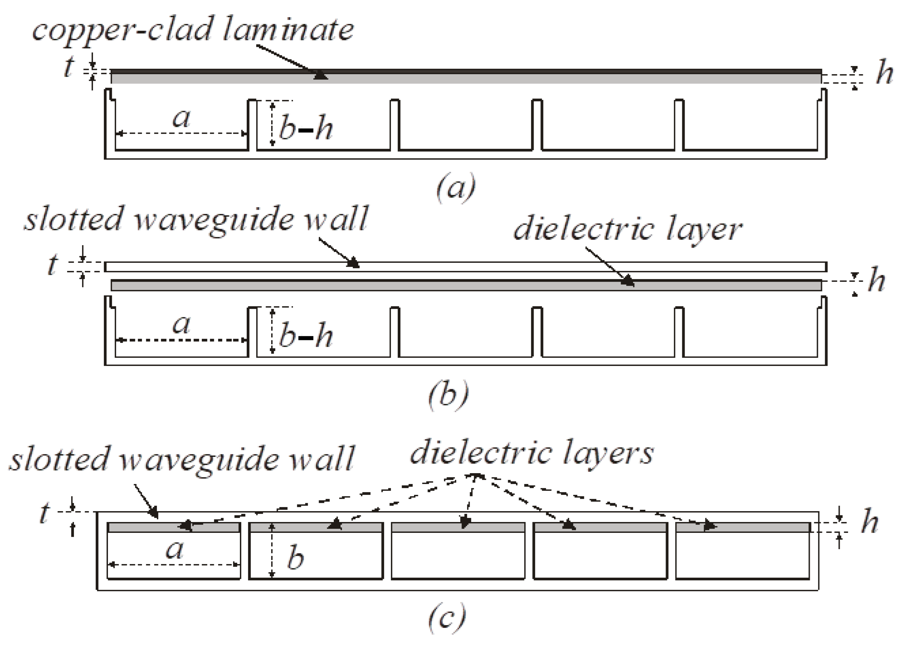
In [4], a copper-clad laminate replaces the upper wall of the radiating waveguide (Figure 3). With this design choice, the waveguide structure becomes easier to realize and more flexible if compared with standard WSAs. This is due to the fact that the performance of the array only depends on the configuration of the slotted laminate, and the laminate can be easily substituted with a negligible production cost if compared with the total array cost, ensuring the same or higher accuracy with respect to typical waveguide slot arrays.
The structure described in [4], whose geometry is reported in Figure 3, is appropriate, especially for a WSA where the radiating waveguides are partially filled with a dielectric substrate. In this case, the copper layer can be positioned above the dielectric laminate (Figure 3a), and therefore the radiating slots radiate in an open half-space in the same way as a classic WSA. Moreover, the etched copper-clad laminate, having the dielectric substrate attached to its bottom part, and which is hence placed inside the waveguide, gives to the structure an important improvement: it allows for keeping the waveguide internal region’s pressurization, increasing the dielectric strength of the air. This feature is extremely useful for several applications of WSAs, such as aerospace applications and RADAR (where high transmission power is usually required).
In many cases, a more robust structure is required in order to keep the waveguide pressurization, and therefore the copper-clad laminate must be substituted with a dielectric sheet, which has to be inserted inside the waveguide and attached to a thick slotted wall (see Figure 3b). It can be deduced that the configuration of the array which is easier to realize is the one having a single dielectric layer, which is common for all the radiating waveguides. Hence, the configuration proposed in [4] and reported in Figure 3 is made of a metallic “comb-like” structure, consisting of the bottom and the sidewalls of the radiating waveguides, which is covered on the upper side by a laminate clad with copper (Figure 3a) or a sheet of dielectric attached to the wall of the slotted waveguide (Figure 3b). Either structures described in Figure 3a,b require a feeding with alternating phases for the radiating waveguides of the WSA in order to avoid deterioration of the array performance, caused by the effect of the internal coupling involving adjacent radiating waveguides. This coupling is due to the common dielectric layer for all the radiating waveguides (so as to get a flexible and cheaper structure, as was already described in this section), and this can be prevented by simply feeding all the radiating waveguides with coupling slots having the same tilt angle.
The insertion of a dielectric layer inside the waveguide gives the structure another important advantage, since it decreases the guided wavelength, hence reducing the array spacing. In fact, the radiating slots must be spaced at half the guided wavelength in a WSA [2] (about 0.7–0.8 λ0 in an empty waveguide, where λ0 is the wavelength in free space). Therefore, the number of slots composing the array (i.e., the number of elements of the array) is limited in an empty waveguide, and in many cases, this could hinder obtaining a satisfying radiation pattern or an adequate aperture distribution. On the other hand, the presence of the dielectric sheet can allow a rise in the number of elements of the array, helping the designer to obtain a better radiation pattern.
The standard Elliot procedure used in the design of a WSA with empty radiating waveguides can be extended for partially filled radiating waveguides fed with alternating phases by computing the slot self-admittance Yn of the design equations in the waveguide partially filled with the dielectric sheet [4].
The extended design procedure presented in [4] neglects the internal mutual coupling between adjacent radiating waveguides. Therefore, each radiating waveguide in the model of the array was treated as if it was separated through metallic sidewalls from the adjacent radiating waveguides. In other words, each radiating waveguide is supposed to have its own dielectric slab (as indicated in Figure 3c). As a consequence, it is possible to analyze the cases depicted in Figure 3a,b with the model in Figure 3c, appropriately choosing the thickness of the region internal to the slot. This thickness must, in fact, be equal to the thickness of the metal in the laminate clad with copper for the case of Figure 3a and to the waveguide wall thickness for the case of Figure 3b.
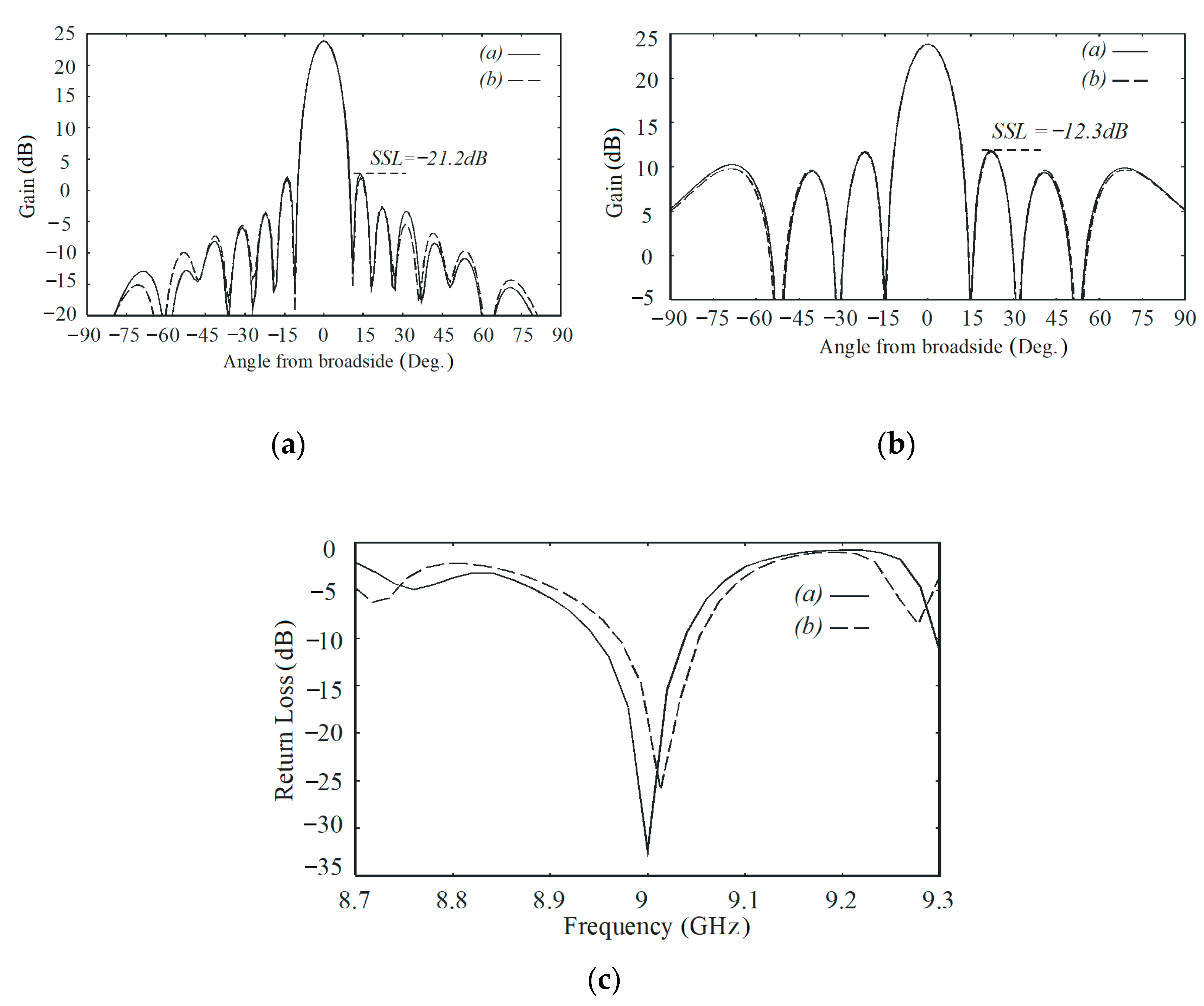
The design procedure described in [4] was applied to the case of a 10 × 5 planar array having a Taylor distribution with 10 elements (and requiring −20 dB sidelobes) in the E-plane and a uniform distribution with 5 elements in the H-plane. In both cases, all the waveguides were WR90, and the arrays were designed at the central frequency of 9 GHz, with the sheet of dielectric having a dielectric permittivity of 2.2 and its thickness being h = 0.508 mm while the slotted wall of the waveguide was 1 mm thick (t = 1 mm).
The designed array (considering both the case of a common dielectric layer (Figure 3a,b) and its corresponding approximate model (Figure 3c)), had a simulated radiation pattern for the E-plane, reported in Figure 4a, and for the H-plane, shown in Figure 4b, while Figure 4c shows the array frequency response. These results highlight that by using alternate phase feeding, it is possible to neglect the effects of the mutual coupling between the radiating waveguides during the design procedure.

4.3. Design of a WSA in a Waveguide Covered with a Dielectric Slab

Many WSA applications require the dielectric sheet to be more properly positioned in the half-space region external to the radiating waveguides rather than inserted into the radiating waveguide. This is a common requirement, for example, in aerospace application, such as supersonic aircraft, guided missiles and space vehicles, where the dielectric slab is used as a covering for protection or as a layer insulating the structure from excessive heat. The standard procedure proposed by Elliott for designing a WSA [2] can be appropriately modified to account for the case of radiating waveguides protected with a covering dielectric sheet (Figure 5.). In this case, the dielectric layer attached to the external metallic wall of the radiating waveguides modifies both the external coupling coefficient between the radiating elements and the self-admittance of each longitudinal radiating slot, which therefore must be accurately recomputed while taking into account the effect of this covering layer.
The circuital and radiating behaviors of a single longitudinal slot in a dielectric-covered waveguide have been described in detail by Mazzarella and Montisci [30] and Katehi [5], while in [6], the external mutual coupling was computed while considering the effect of the dielectric cover, allowing extension of the design procedure proposed by Elliott to the case of a WSA with dielectric-covered radiating waveguides.
When the slots radiate in free space (i.e., the radiating waveguide is not covered by a dielectric layer), the normalized coupling coefficient gnm in the second design’s Equation (2) can be computed as described in [22]. This expression cannot be used when the radiating waveguides are covered with a dielectric slab and must therefore be recomputed while including the effect of the external dielectric sheet. The resulting expression of the mutual coupling coefficient for a waveguide covered with a dielectric slab can be written as [6]
g n m = A j ω ε S l o t   m [ F _ e x t [ M _ n ] M _ m + 1 k 2 ( F _ e x t [ M _ n ] ) ( M _ m ) ] d S
where A is an appropriate normalization coefficient, Mn and Mm are the normalized equivalent magnetic currents on the slot apertures “n” and “m”, respectively (as indicated in Figure 2b), Fext[Mn] is the vector potential in the region external to the waveguide due to the equivalent magnetic current Mn and k2 = ω2εμ.
In the space domain, the Green function related to the vector potential F cannot be computed in its closed form. Therefore, we must evaluate Equation (5) by resorting to the spectral domain. Using the Parseval identity, we can write
g n m = A j ω ε ( 2 π ) 2 + + [ { F _ e x t [ M _ n ] } { M _ m } + 1 k 2 { F _ e x t [ M _ n ] } { M _ m } ] d u d v
where u and v are the spectral variables conjugate of the space variables x and z and is the Fourier transform operator. Byetting u = k0ρsin(ϕ) and v = k0ρcos(ϕ), Equation (4) can be computed by splitting the domain of integration into three subdomains:
i )   ( ρ , φ ) [ 0 , 1 ] × [ π , π ] ; i i )   ( ρ , φ ) [ 1 , ε r ] × [ π , π ] ; i i i )   ( ρ , φ ) [ ε r , ] × [ π , π ]
This is performed to consider the effect of the pole caused by the propagation of the TM0 mode (corresponding to the surface wave traveling into the dielectric layer) [6]. While in the subdomains (i) and (ii), the corresponding integrals in Equation (6) can be computed with a standard Gaussian quadrature after adequate changes of the variable [6]. The evaluation of the integral in the unbounded subdomain (iii) in particular requires attention and must be carefully evaluated by applying adequate mathematical concepts. We can write the integral (6) as
π + π [ ε r + [ f ( ρ , φ ) ] exp { j k 0 ρ ( Δ x n m cos ( φ ) + Δ z n m sin ( φ ) ) } d ρ ] d φ
where in d n m = Δ x n m 2 + Δ z n m 2 is the distance between the generic slots “n” and “m” of the array (Figure 2b).
Since the integrand, with respect to the variable ρ in Equation (7), rapidly oscillates for increasing values of ρ, its convergence decreases, becoming slower for increasing values of dnm, the distance between the “n-th and “m-th slots of the array. The convergence of this integral can be accelerated by resorting to the weighted average algorithm (WAA) together with the Shank’s transform, as described in detail in [6].
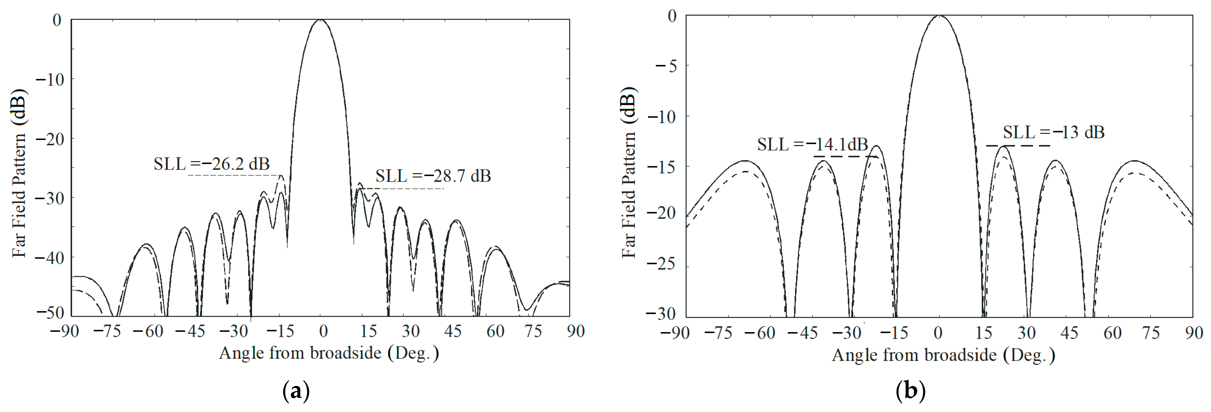
This design procedure has been applied to a planar array with 10 × 5 elements requiring a Chebychev distribution (having an SLL of −30dB) with 10 elements in the H-plane and a uniform distribution with 5 elements in the E-plane. The modified design procedure, including the dielectric cover effect in the computation of the external mutual coupling, was compared with the standard design procedure, which does not take into account the influence of this dielectric cover on the array behavior [6].
In the presented example, feeding and radiating waveguides are both half-height WR90 (with a transverse section having dimensions of 22.86 mm × 5.08 mm), and their wall thickness is 1 mm with a design frequency of 9 GHz. The dielectric slab thickness is h = 0.381 mm, and its dielectric permittivity is 2.2. The length of all the coupling slots is 17.1 mm, their width is 1.5 mm, and the tilt angle with regard to the axis of the feeding waveguide is 22.6°, which leads to a coupling coefficient of 0.5.
The lengths and offsets of the designed slots, both computed through the extended procedure including the external dielectric coupling and using the standard design procedure (where coupling is evaluated as if the slots radiate in free space, and which we can hence call “free space coupling”) are indicated in [6].
Figure 6a,b reports the far-field patterns simulated with High Frequency Simulation Software (HFSS) for the designed array, while Figure 6c shows its frequency response. Figure 6 shows the comparison between the case of “dielectric coupling” and that of “free space coupling”, highlighting the significant improvement in the array performance obtained using the tailored synthesis procedure. In particular, the array designed considering the influence of the dielectric cover in the evaluation of the external mutual coupling had a −13 dB SLL in the E-plane (with a nominal uniform pattern) and a −28.7 dB SLL in the H-plane (with a nominal −30dB Chebichev distribution). On the other hand, the corresponding SLL values for the “free space coupling” were −14 dB and −26.2 dB, respectively. In addition, the frequency response for “dielectric coupling” had better behavior, with a minimum reflection coefficient equal to −30dB at the design frequency, while it increased to −22 dB for the case of “free space coupling”.
The convergence of the integral expressing the mutual coupling in Equation (7) rapidly worsened for increasing slot distances, and this can be a severe limitation in the design of large arrays, since its calculation becomes even more time-consuming. Therefore, it is difficult to maintain the desired accuracy for big distances between the radiating slots. In addition, the correct implementation of the WAA calls for a deep investigation of the behavior of the integrand function, strongly decreasing the spectral domain approach’s efficiency and robustness. This is mainly due to the fact that the oscillation period is related by means of a complicated relation to the slot distance, and the WAA should be appropriately tailored to this behavior to properly ensure the convergence of this integral. In order to avoid these drawbacks, the external mutual coupling can be directly computed in the spatial domain, resorting to the discrete complex image method (DCIM) [43]. The DCIM requires a computational time significantly smaller than the spectral domain procedure for an accurate evaluation of the mutual coupling, also giving a computational time and an accuracy which are independent from the slot distance. Therefore, the use of DCIM does not need any particular treatment for large slot distances, as is required instead for the case of the spectral domain approach.

4.4. Multilayer Dielectric Cover Effect in WSAs

In several applications, the model of a single-layer dielectric-cover cannot be used, and WSAs with multilayer dielectric covers are required. This is the case, for example, with flat sandwich radomes, which are mainly used for thermal insulation and protection [80], increasing the radiating waveguides’ pressurization or even for aerodynamic purposes in several WSA applications, and eventually also for coatings with layers of paint. Therefore, the circuital properties of a radiating slot cut in a waveguide implemented with a multilayer dielectric cover were investigated [7].
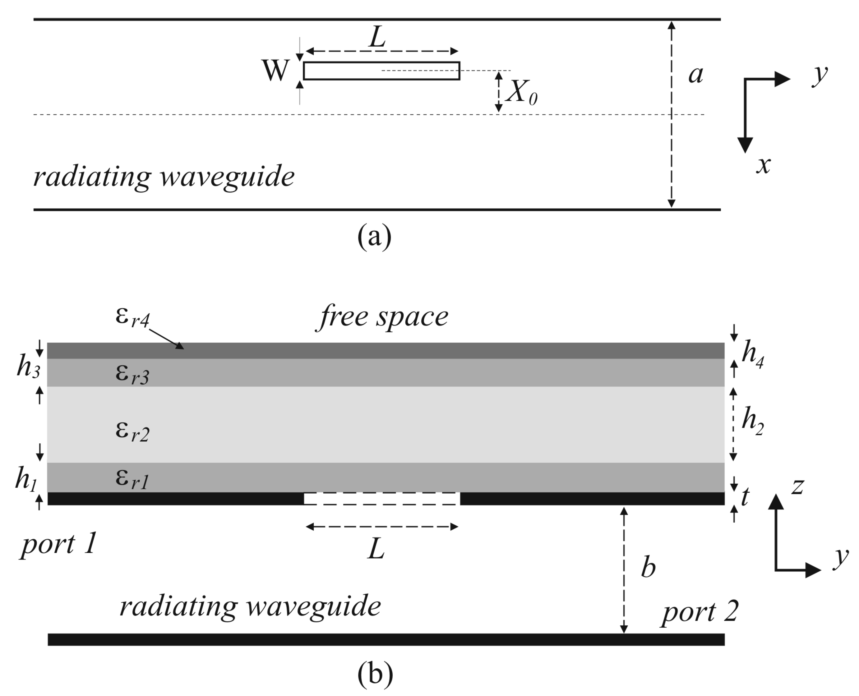
As an example of the layout of a WSA with a multilayer dielectric cover, in Figure 7, the longitudinal radiating slot (shown in Figure 6a) is covered with four dielectric layers, having thicknesses equal to h1, h2, h3 and h4 and relative permittivity equal to εr1, εr2, εr3 and εr4.
Usually, the dielectric covering structures are applied to the WSA after its design and realization. Hence, the shape and dielectric and geometrical properties of these covering layers are chosen to minimize their effect on the WSA’s circuital and radiating properties, rather than being optimized for their effective purpose. A more effective and better solution is the “embedding” of this radome structure in the WSA by including the multilayer dielectric cover directly in the analysis and design procedures of the array. This way, the dielectric properties and the geometry of the radome can be determined in order to optimize the array protection, its thermal insulation and eventually also the radiating waveguides’ pressurization [7].
An effective and accurate model for a radiating slot cut in a multilayer dielectric-covered waveguide is therefore required, namely one which allows analyzing a dielectric cover with a generic number of layers N. The effect of the presence of an arbitrary radome structure on the performance of a longitudinal slot was detailed and evaluated in [7], where several configurations of multilayer dielectric covers were considered for a radiating slot in a WSA working in the X-band, focusing the discussion on the most typical practical cases. The procedure described in [7] can be exploited by waveguide slot antenna designers during the design phase, since it allows for estimating the effects of the radome structure on the radiating performance of the longitudinal slot, and this can significantly ease the design of a multilayer dielectric-covered WSA. In particular, it is possible to evaluate if, given a certain configuration of the dielectric cover, the circuital and radiating behavior of the slot can be reasonably assumed to be independent from the properties of one or more covering layers.
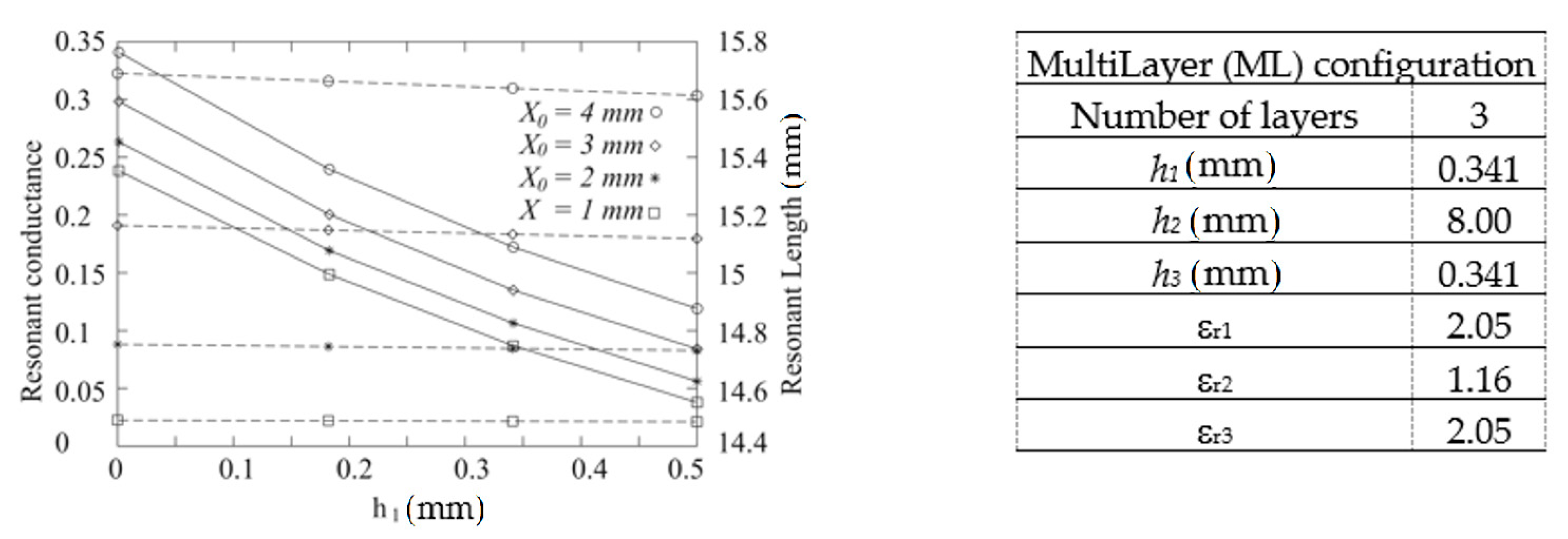
Let us consider, as an example, a WSA covered with three dielectric layers. In a typical configuration, the first layer of a sandwich radome can be used as a cap for the radiating slots, allowing radiating waveguide pressurization. The thickness of this layer must be determined to guarantee an adequate strength when high-pressure air is necessary for into the waveguide. The second layer is instead a foam with low dielectric permittivity, and its thickness is chosen to reach adequate thermal insulation of the WSA. The third layer is used essentially for aerodynamic and protection purposes. In Figure 8 and Figure 9, the configuration of the dielectric layers covering the WSA is reported. The images show the variation of the slot resonant length and of the normalized conductance at the resonant frequency (9 GHz) with respect to the thickness of the first (h1) and second (h2) covering layers, respectively. In both figures, X0 represents the offset of the slot with respect to the center of the radiating waveguide, as shown in Figure 7a.
As is described in [7] and reported in Figure 8, the resonant length of the radiating slot is inversely proportional to the first layer’s thickness, whereas it increases with the second layer’s thickness (Figure 9). This behavior is due to the fact that, in the analyzed configuration, the second layer has a dielectric permittivity smaller than the third layer. Therefore, the equivalent permittivity seen by the slot diminishes when the thicknesses increase. In both cases (Figure 8 and Figure 9), the conductance of the slot computed at resonance was nearly constant with respect to h1 and h2.
Usually, a WSA also requires a paint layer in the sandwich radome, and therefore a fourth layer should be added to the previously analyzed configuration. On the other hand, both the slot resonant length and its normalized conductance at the resonant frequency can be considered independent from the fourth layer’s thickness if this thickness is within the range of 0–150 µm. Hence, under the appropriate conditions, which depend on the thickness of the second layer (the insulating layer in this case), we could neglect this fourth layer during the WSA design.
As was demonstrated in [81], an accurate choice of the configuration of the multilayer dielectric cover can be exploited to improve the aperture efficiency and the gain of the designed array. Additionally, it allows to benefit of the radome structure, which ensures the WSA’s adequate protection, pressurization of the radiating waveguides and thermal insulation. However, most importantly, a suitable choice of the structure of the multilayer dielectric cover can allow the designer to reduce the number of the radiating slots if compared with a WSA radiating in free space and having the same efficiency and gain. This represents a valuable improvement for the WSA because it directly affects the production cost (which is very high with respect to, for example, microstrip patch antennas). As a matter of fact, the small fabrication cost increment required for an optimized dielectric-covered array is vastly overcompensated by the savings due to the diminished number of both radiating slots and guides. Moreover, the consequent simplification of the waveguide network which feeds the array allows for more compact solutions.
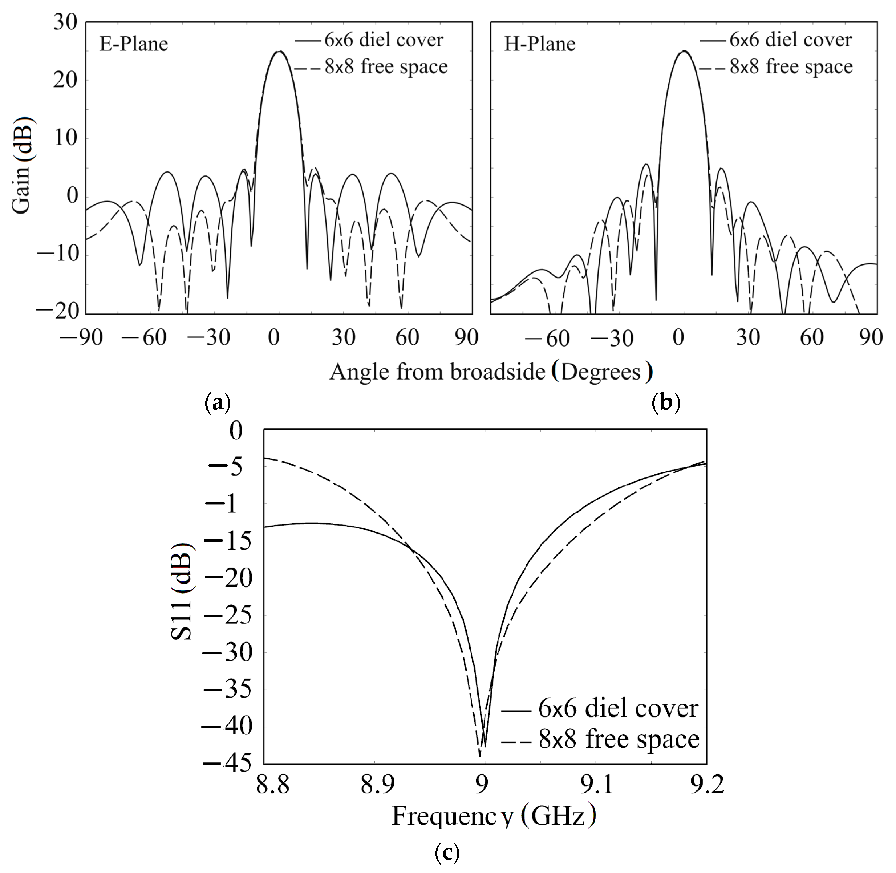
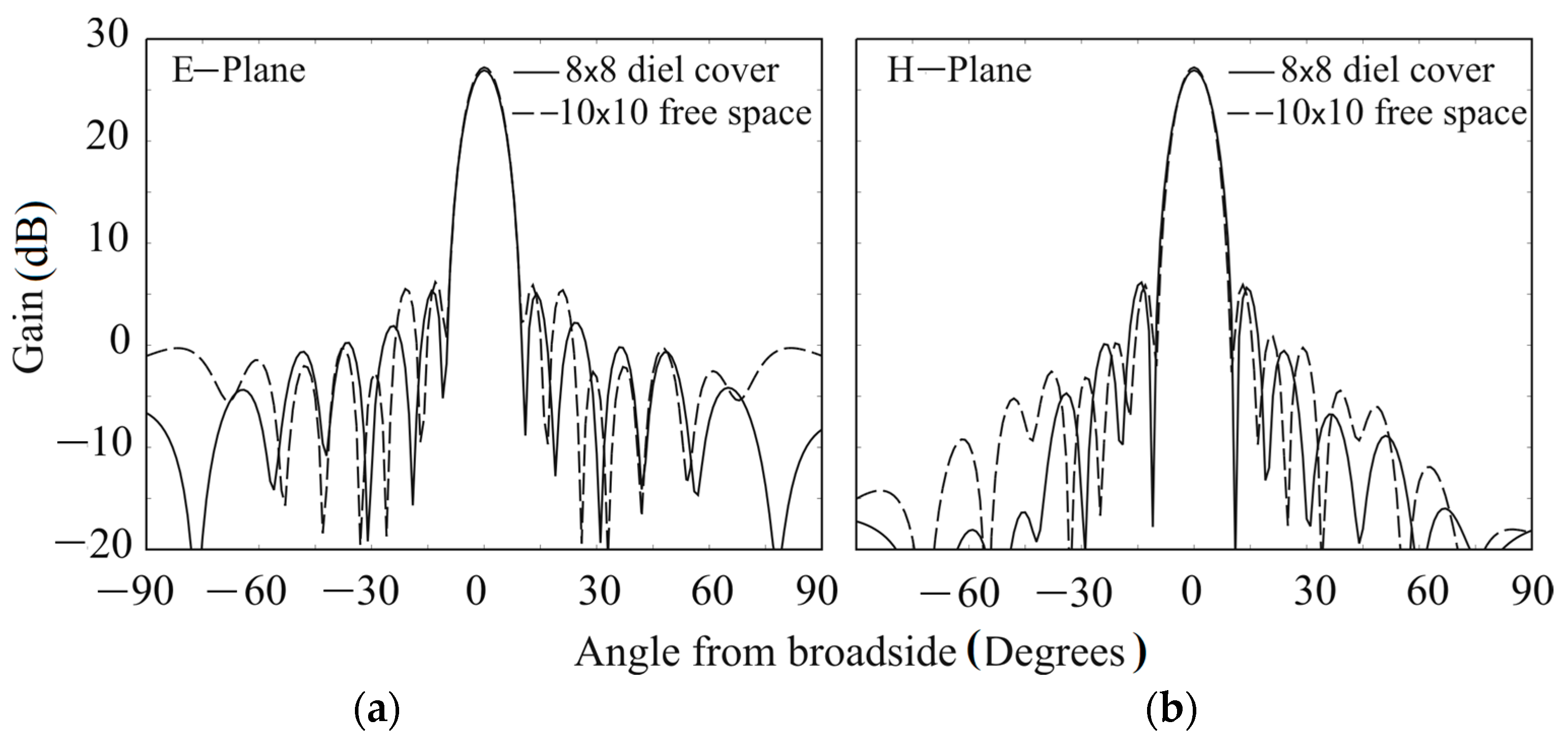
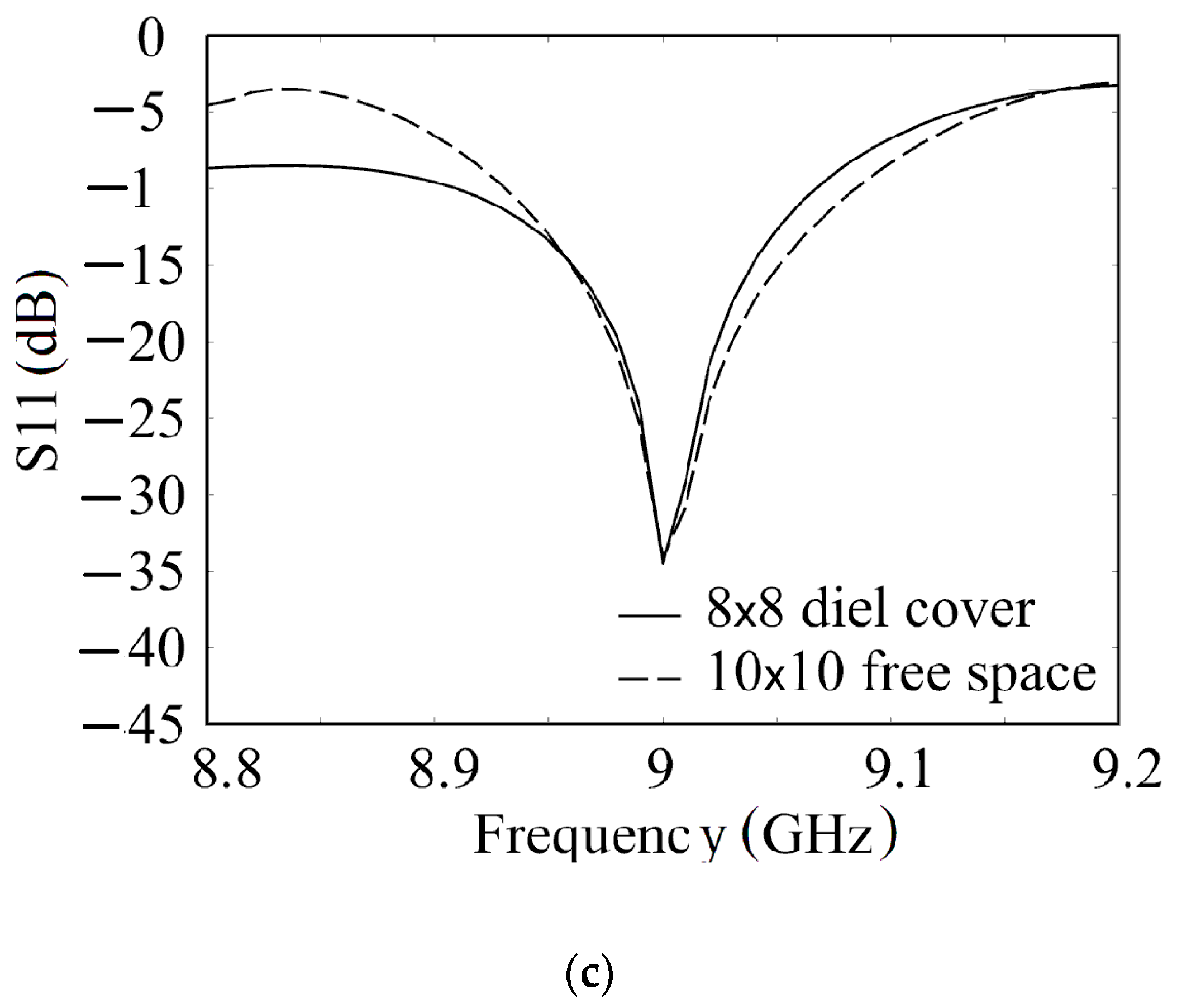
In [81], a suitably designed dielectric cover is described which allows for a significant reduction of the number of radiating slots (by about 30%) with no degradation of the performance of the array. The proposed solution was tested on three different planar arrays with 6 × 6 elements (having a two-layer dielectric cover), 8 × 8 elements (having a two-layer dielectric cover and radiating into free space) and 10 × 10 elements (radiating into free space). In that paper, the basic configuration consisting of a dielectric cover with two layers was chosen (the array geometry is reported in Figure 10), according to [82], where the first layer was a substrate with a low dielectric permittivity (such as air or foam) and had an appropriate thickness, whereas the second layer was a high-dielectric permittivity substrate which acted as a partially reflecting sheet. The resulting comparisons are reported in Figure 11 and Figure 12 (where the frequency response and the radiation patterns in the E-plane and H-plane are shown). The presented results confirm that an array with 8 × 8 elements which radiates in free space exhibits the same frequency bandwidth and radiating properties of an array containing 6 × 6 elements with a dielectric cover (Figure 11), and that an array with 10 × 10 elements which radiates in free space has the same behavior as an array with 8 × 8 elements and a dielectric cover (Figure 12), highlighting the performance improvement of the WSA thanks to the multilayer dielectric cover.

4.5. Interaction between the Beam-Forming Network and the Radiating Waveguides

The behavior of a planar WSA, in terms of the radiated field and frequency response, is influenced by a multitude of effects of the second order in the beam forming network [11,12,13]. The most significant ones are the interaction between the radiating slots in the radiating waveguides and the slot couplers between radiating and feeding waveguides, the interaction due to the higher-order mode between the coupling slots and the interaction between the waveguide bends and the nearest slot couplers in the feeding waveguides. Hence, in order to design a high-performance WSA, more accurate and adequate design procedures must be devised, which can be derived by a suitable modification of the Elliott model used to design a standard WSA [11,12,13]. In [11,12,13], the extension of the Elliot procedure, taking into account the second-order effects in the planar WSA, is presented, and it includes the following:
  • The strong influence between the T-junction and the coupling slots which connect the radiating and feeding waveguide;
  • The interaction between the coupling slot and the nearby radiating slots;
  • The effect of the bent terminations.
In addition to these effects, in [83], an efficient design procedure is described that is able to compensate for higher-order mode coupling between inclined coupling slots and neighboring radiating slots. This compensation is obtained with only a minimal cost to the design complexity and consists of adding closed-form terms to the expression for the active admittance of radiating slots. The results of this modification are minor adjustments to the dimensions of the slot radiators, which effectively improve the amplitude accuracy and phase consistency of element excitations, which can be crucial, especially when designing shaped beam arrays [5].
Effects i–iii produce a non-negligible increment of the level of the first sidelobes comparable to an ideal WSA (until 5–6 dB), and this causes a significant degradation in the array’s performance. Hence, they must be considered in the design of a WSA with high performance, such as a WSA requiring a reduced SLL. As an example, if we consider high-performance radar systems, they require ultra-low sidelobe antennas [15,84,85,86,87], characterized by a very low level of the sidelobes with respect to the usual SLL required for standard radar applications. In these applications, even an increment of the near sidelobes of only a couple of dBs, or a prediction of their topography with an inadequate accuracy, can result in unsatisfying behavior.
In addition, in many radar applications, the WSA is split into sub-arrays, because this design choice allows for augmenting the array frequency bandwidth. In these structures, each sub-array can be fed using a T-junction [12,13] or by an inclined coupling slot [11,13,88,89]. The former solution is a common choice for monopulse arrays, where planar arrays are fed by one or more T-junctions positioned in the E-plane of the array. This kind of array requires each feeding guide to end with a shorted termination, which must have a length equal to half a wavelength beyond the last coupling slot. This shorted bend is commonly implemented with an “L” or “U” bend, which influences the behavior of the coupling slot itself [13]. Such (and similar) applications call for an appropriate characterization and design of planar WSAs for high-performance systems.
In order to take into account the second-order effects i–iii and include them into a tailored analysis procedure, the first step consists of devising an appropriate model for each specific effect through an opportune matrix model (a hybrid matrix). Afterward, the set of equations derived by this matrix model must be adequately included into the equations used to describe the behavior of the array [13].
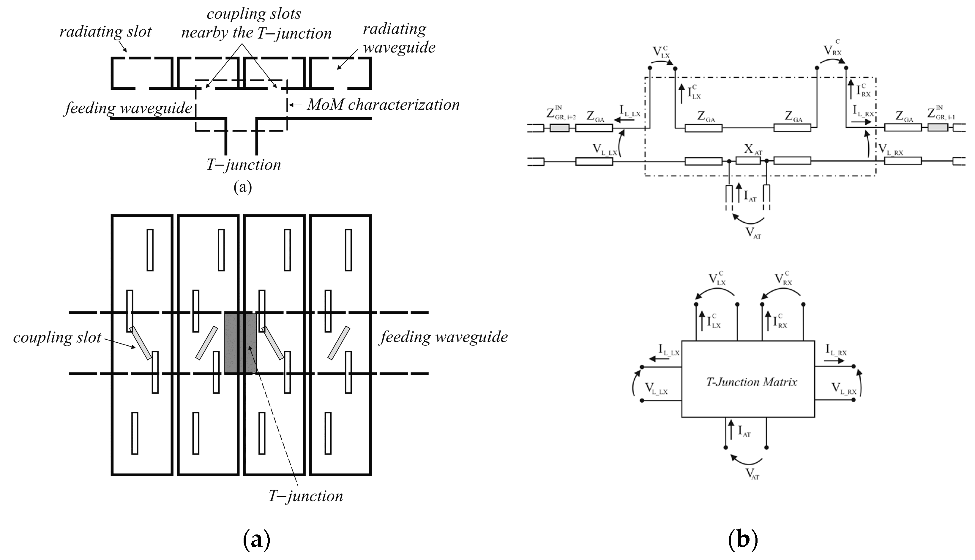
Here, we limit the discussion to effect i, whereas the detailed descriptions of effects ii and iii can be found in [13]. The interaction between the T-junction and the nearest slot couplers that belong to the feeding network of the array can be described by modeling the T-junction through a five-port network (Figure 13). In Figure 13b, which represents the T-junction equivalent circuit and matrix model, IL and VL indicate the current and the voltage along the feeding waveguide, respectively, immediately to the left (subscript LX) or to the right (subscript DX) of the slot couplers near the T-junction. IC and VC indicate the current and the voltage, respectively, in the slot couplers near the T-junction. IAT (or VAT) is the feeding known term at the T-junction. The radiating waveguides farthest from the T-junction are replaced in Figure 13b by their input impedance (i.e., the impedance seen looking at the input port of their slot coupler). The T-junction can therefore be modeled by the following hybrid matrix, which corresponds to the equivalent circuit of Figure 13b:
{ V A T = Z 11 I A T + S 12 V L _ L X + S 13 V L _ R X + S 14 V R X C + S 15 V L X C I L _ S X = A 21 I A T + Y 22 V L _ L X + Y 23 V L _ R X + Y 24 V R X C + Y 25 V L X C I L _ D X = A 31 I A T + Y 32 V L _ L X + Y 33 V L _ R X + Y 34 V R X C + Y 35 V L X C I D X C = A 41 I A T + Y 42 V L _ L X + Y 43 V L _ R X + Y 44 V R X C + Y 45 V L X C I S X C = A 51 I A T + Y 52 V L _ L X + Y 53 V L _ R X + Y 54 V R X C + Y 55 V L X C
wherein Zij are the impedances, Yij are the admittances and Sij and Aij are adimensional coefficients. All these coefficients of the 5 × 5 hybrid matrix are calculated using a method of moments (MoM) procedure which allows for analyzing the structure of Figure 13a.
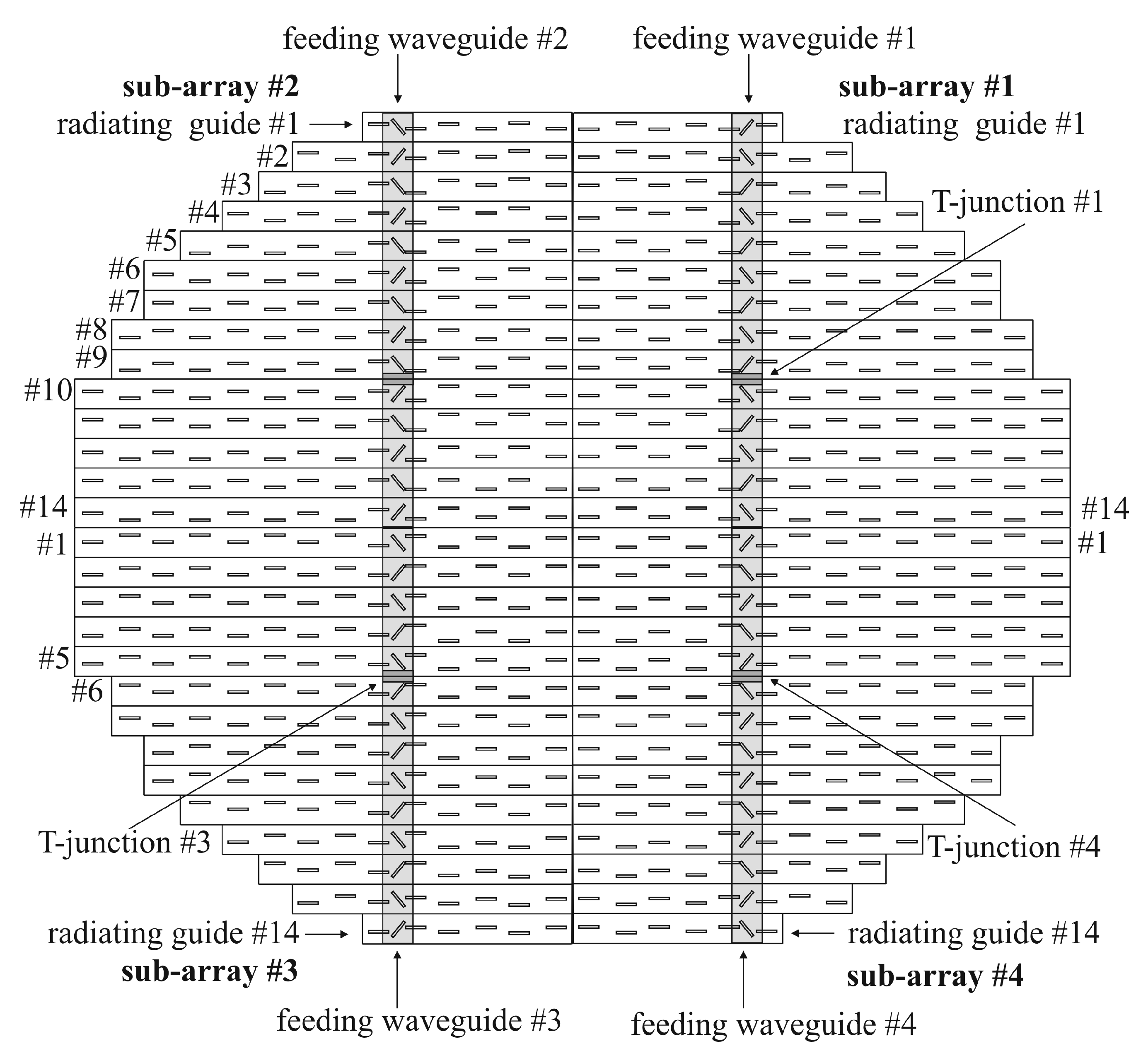
The results of the procedure presented in [13], which included the second-order effects i–iii in the analysis of a planar WSA, were compared with the measured data of a prototype realized by Selex Galileo, consisting of a monopulse array designed to work at the X-band, having a diameter of 72 cm and the geometry shown in Figure 14. This array is formed by 56 radiating waveguides, each one having a different number of radiating slots, and it is split into 4 sub-arrays. The array is composed of a total of 656 radiating slots, with a beam-forming network consisting of 56 inclined coupling slots. Each of the four sub-arrays is fed by a waveguide through the coupling slots, and each feeding waveguide, which ends with two shorted bends (one for each side), is fed in turn by a T-junction as shown in Figure 14. The T-junctions are placed between the ninth and tenth radiating waveguides for sub-arrays 1 and 2, and between the fifth and sixth radiating waveguides for sub-arrays 3 and 4, with an array structure of (9-5, 5-9, 9-5, 5-9).
The nominal pattern of the array shown in Figure 14 is a Taylor distribution having an SLL equal to −30 dB in both the H-plane and the E-plane. The array’s E-plane far-field pattern is reported in Figure 15. Figure 15 shows that the behavior of the array was predicted in a very satisfying and accurate way using the improved analysis model, which gave results close to the measured data. The interferences between the coupler, the bent terminations and the nearby radiating slots caused a variation of a couple percent in the excitation amplitude and of 5–10° in the excitation phase of these radiating slots with respect to the “ideal” case, and this modification in the slot excitations resulted in a significant increase of the first-level sidelobes. The far-field pattern had significant degradation only in the array’s E-plane, whereas the H-plane (whose far-field diagrams were not reported here for this reason) was not influenced by the interaction between the radiating and coupling slots, which resulted only in a slight modification of its sidelobes.
Finally, in order to summarize the parameters of the state-of-the-art works, the advantages of the WSA configurations described in this review are reported in Table 2, and Table 3 compares a large number of WSAs with different configurations in terms of the number of elements, aperture size, return loss bandwidth, axial ratio bandwidth, gain bandwidth, peak gain, efficiency and sidelobe level.

5. Conclusions

This work presents a review which was focused mainly on the improved available design techniques proposed in the literature to obtain waveguide slot arrays with high performance, highlighting the most important limitations and drawbacks of such arrays along with possible effective countermeasures.
The main topics addressed in this review were as follows: partially filled or covered WSAs with a multilayer dielectric sheet, useful for insulating or protecting the structure from unfavorable environmental conditions, and increasing the waveguide peak power, array efficiency and gain. In addition, the most prominent effects of the second order in the planar array feeding network (such as the effect of the interaction between each slot coupler of the feeding network and the radiating slots nearest to this coupler, the effect of the feeding T-junction on the array performance and the effects of the waveguide bends) were accurately discussed. All these second-order effects can critically increase the first sidelobes if compared to the ideal case, causing a sensible worsening in the performance of the array, and must be considered in the array design.

Author Contributions

Conceptualization, G.A.C.; methodology, G.A.C. and G.M. (Giorgio Montisci); formal analysis, G.A.C., G.M. (Giuseppe Mazzarella) and G.M. (Giorgio Montisci); investigation, G.A.C.; resources, G.A.C.; data curation, G.A.C. and G.M. (Giorgio Montisci); writing—original draft preparation, G.A.C..; writing—review and editing, G.A.C. and G.M. (Giacomo Muntoni); visualization, G.A.C. and G.M. (Giacomo Muntoni); supervision, G.A.C. and G.M. (Giuseppe Mazzarella). All authors have read and agreed to the published version of the manuscript.

Funding

This research received no external funding.

Conflicts of Interest

The authors declare no conflict of interest.

References

  1. Watson, W.H. The Physical Principles of Waveguide Transmission and Antenna Systems; Clarendon Press: Oxford, UK, 1947. [Google Scholar]
  2. Elliott, R.S. Antenna Theory and Design; Prentice-Hall: New York, NY, USA, 1981. [Google Scholar]
  3. Johnson, R.C.; Jasik, H. Antenna Engineering Handbook; McGraw-Hill: New York, NY, USA, 1984. [Google Scholar]
  4. Casula, G.A.; Mazzarella, G.; Montisci, G. Design of slot arrays in waveguide partially filled with dielectric slab. Electron. Lett. 2006, 42, 730. [Google Scholar] [CrossRef]
  5. Katehi, P. Dielectric-covered waveguide longitudinal slots with finite wall thickness. IEEE Trans. Antennas Propag. 1990, 38, 1039–1045. [Google Scholar] [CrossRef]
  6. Casula, G.A.; Montisci, G. Design of Dielectric-Covered Planar Arrays of Longitudinal Slots. IEEE Antennas Wirel. Propag. Lett. 2009, 8, 752–755. [Google Scholar] [CrossRef]
  7. Jin, Z.; Montisci, G.; Mazzarella, G.; Li, M.; Yang, H.; Casula, G.A. Effect of a multilayer Dielectric Cover on the Behavior of Waveguide Longitudinal Slots. IEEE Antennas Wirel. Propag. Lett. 2013, 11, 1190–1193. [Google Scholar] [CrossRef]
  8. Orta, R.; Tascone, R.; Zich, R. Performance degradation of dielectric radome covered antennas. IEEE Trans. Antennas Propag. 1988, 36, 1707–1713. [Google Scholar] [CrossRef]
  9. Hirokawa, J.; Ando, M.; Goto, N. Waveguide-fed parallel plate slot array antenna. IEEE Trans. Antennas Propag. 1992, 40, 218–223. [Google Scholar] [CrossRef]
  10. Casula, G.A.; Mazzarella, G.; Montisci, G. Design of shaped beam planar arrays of waveguide longitudinal slots. Int. J Antennas Propag. 2013, 2013, 767342. Available online: https://www.hindawi.com/journals/ijap/2013/767342/ (accessed on 21 February 2013). [CrossRef]
  11. Casula, G.A.; Mazzarella, G. A Direct Computation of the Frequency Response of Planar Waveguide Slot Arrays. IEEE Trans. Antennas Propag. 2004, 52, 1909–1912. [Google Scholar] [CrossRef]
  12. Casula, G.A.; Mazzarella, G.; Montisci, G. Effect of the feedingT-junctions in the performance of planar waveguide slot arrays. IEEE Antennas Wirel. Propag. Lett. 2012, 11, 953–956. [Google Scholar] [CrossRef]
  13. Casula, G.A.; Montisci, G.; Mazzarella, G.; Maxia, P.; Fanti, A. Improved analysis of high-performances planar waveguide slot arrays. J. Electromagn. Waves Appl. 2013, 27, 2155–2165. [Google Scholar] [CrossRef]
  14. Rengarajan, R.S.; Shaw, G.M. Accurate characterization of coupling junctions in waveguide-fed planar slot arrays. IEEE Trans. Microw. Theory Tech. 1994, 42, 2239–2247. [Google Scholar] [CrossRef]
  15. Schrank, H. Low sidelobe phased array antennas. IEEE Antennas Propag. Soc. Newsl. 1983, 25, 4–9. [Google Scholar] [CrossRef]
  16. Silver, S. Microwave antenna Theory and Design; Dover Publications: New York, NY, USA, 1965. [Google Scholar]
  17. Stevenson, A.F. Theory of Slots in Rectangular Wave-Guides. J. Appl. Phys. 1948, 19, 24–38. [Google Scholar] [CrossRef]
  18. Stegen, R.J. Longitudinal Shunt Slot Characteristics; Technical Report 261; Hughes Technical Memorandum: Culver City, CA, USA, 1971. [Google Scholar]
  19. Oliner, A.A. The impedance properties of narrow radiating slots in the broad face of rectangular waveguide, Part I theory. IRE Trans. Antennas Propag. 1957, 5, 4–20. [Google Scholar] [CrossRef]
  20. Yee, Y. Impedance of a Narrow Longitudinal Shut Slot in a Slotted Waveguide Array. IEEE Trans. Antennas Propag. 1974, 22, 589–592. [Google Scholar]
  21. Khac, T.V.; Carson, C. Impedance properties of a longitudinal slot antenna in the broad face of a rectangular waveguide. IRE Trans. Antennas Propag. 1973, 21, 708–710. [Google Scholar] [CrossRef]
  22. Elliott, R. An improved design procedure for small arrays of shunt slots. Antennas Propag. Soc. Int. Symp. 2005, 31, 48–53. [Google Scholar] [CrossRef]
  23. Elliott, R. On the design of traveling-wave-fed longitudinal shunt slot arrays. Antennas Propag. Soc. Int. Symp. 2005, 7, 717–720. [Google Scholar] [CrossRef]
  24. Elliott, R.; O’Loughlin, W. The design of slot arrays including internal mutual coupling. IEEE Trans. Antennas Propag. 1986, 34, 1149–1154. [Google Scholar] [CrossRef]
  25. Hansen, R.C.; Brunner, G. Dipole Mutual Impedance for Design of Slot Arrays. Microw. J. 1979, 22, 54–56. [Google Scholar]
  26. Mazzarella, G.; Panariello, G. On the evaluation of mutual coupling between slots. IRE Trans. Antennas Propag. 1987, 35, 1289–1293. [Google Scholar] [CrossRef]
  27. Mazzarella, G.; Panariello, G. Design of slot arrays for SAR applications. Alta Freq. 1986, 55, 359–364. [Google Scholar]
  28. Mazzarella, G.; Panariello, G. Evaluation of edge effects in slot arrays using the geometrical theory of diffraction. IEEE Trans. Antennas Propag. 1989, 37, 392–395. [Google Scholar] [CrossRef]
  29. Josefsson, L. Mutual coupling calculations including edge effects. Electron. Lett. 1994, 30, 2087–2088. [Google Scholar] [CrossRef]
  30. Mazzarella, G.; Montisci, G. A Rigorous Analysis of Dielectric-Covered Narrow Longitudinal Shunt Slots with Finite Wall Thickness. Electromagnetics 1999, 19, 407–418. [Google Scholar] [CrossRef]
  31. Rengarajan, S. Scattering characteristics of a centred-inclined slot in a broad wall of a rectangular waveguide. IEE Proc. H Microw. Antennas Propag. 1990, 137, 343. [Google Scholar] [CrossRef]
  32. Montisci, G. Design of Circularly Polarized Waveguide Slot Linear Arrays. IEEE Trans. Antennas Propag. 2006, 54, 3025–3029. [Google Scholar] [CrossRef]
  33. Ferrando-Rocher, M.; Herranz-Herruzo, J.I.; Valero-Nogueira, A. Wideband Coffee-Bean Shaped Radiating Element for Circularly-Polarized Waveguide Slot Arrays. In Proceedings of the 2021 15th European Conference on Antennas and Propagation (EuCAP), Düsseldorf, Germany, 22–26 March 2021; pp. 1–4. [Google Scholar]
  34. Herranz-Herruzo, J.I.; Ferrando-Rocher, M.; Valero-Nogueira, A.; Bernardo-Clemente, B. Novel Asymmetric T-Shaped Radiating Element for Circularly-Polarized Waveguide Slot Arrays. IEEE Trans. Antennas Propag. 2021. [Google Scholar] [CrossRef]
  35. Rengarajan, S.R.; Josefsson, L.G.; Elliott, R.S. Waveguide-Fed Slot Antennas and Arrays: A Review. Electromagn. 1999, 19, 3–22. [Google Scholar] [CrossRef]
  36. Ren, W.; Gao, B.-Q.; Xue, Z.-H.; Li, W.-M.; Liu, B. Full wave analysis of broadwall slot’s character-istics in rectangular waveguides. IEEE Trans. Antennas Propagat. 2004, 52, 2436–2444. [Google Scholar] [CrossRef]
  37. Montisci, G.; Mazzarella, G. Effect of the Longitudinal Component of the Aperture Electric Field on the Analysis of Waveguide Longitudinal Slots. IEEE Trans. Antennas Propag. 2011, 59, 4334–4337. [Google Scholar] [CrossRef]
  38. Li, J.L.-W.; Li, L. Smaller offset broadwall longitudinal waveguide slots: A new analysis using a new idea. IEE Proc. Microw. Antennas Propag. 2005, 152, 179. [Google Scholar] [CrossRef]
  39. Bailey, M. Design of dielectric-covered resonant slots in a rectangular waveguide. IEEE Trans. Antennas Propag. 1967, 15, 594–598. [Google Scholar] [CrossRef]
  40. Bailey, M.C. The impedance properties of narrow radiating slots on the broad face of a rectangular waveguide. IEEE Trans. Antennas Propagat. 1970, 18, 596–603. [Google Scholar] [CrossRef]
  41. Rexberg, L. Vector fourier transform analysis of dielectric-covered slot in the broad wall of a waveguide. Microw. Opt. Technol. Lett. 1988, 1, 360–363. [Google Scholar] [CrossRef]
  42. Mazzarella, G.; Montisci, G. Full-wave analysis of dielectric-covered radiating series slots. Microw. Opt. Technol. Lett. 1999, 20, 67–72. [Google Scholar] [CrossRef]
  43. Jin, Z.; Montisci, G.; Casula, G.A.; Yang, H.; Lu, J. Efficient evaluation of the external mutual coupling in dielec-tric-covered waveguide slot arrays. Int. J. Antennas Propag. 2012, 2012, 7. [Google Scholar] [CrossRef] [Green Version]
  44. Amiri, N.; Forooraghi, K. Analysis of a Dielectric-Covered Waveguide Slot Antenna Using the Spectrum of Two-Dimensional Solutions. IEEE Trans. Antennas Propag. 2014, 62, 3818–3823. [Google Scholar] [CrossRef]
  45. Sanchez-Olivares, P.; Hernandez-Ortega, J.; Masa-Campos, J.L. Mechanically reconfigurable waveguide-slot single element using tuning screws. In Proceedings of the 2017 11th European Conference on Antennas and Propagation (EUCAP), Paris, France, 19–24 March 2017; pp. 1962–1966. [Google Scholar]
  46. Green, J. Asymmetric Ridge Waveguide Radiating Element for a Scanned Planar Array. IEEE Trans. Antennas Propag. 1990, 1161. [Google Scholar] [CrossRef]
  47. Li, T.; Boes, F.; Schneider, K.; Zwick, T. Gap-Waveguide Cavity Slot Array Based on Two Metal Layers at 120 GHz. In Proceedings of the 2020 50th European Microwave Conference (EuMC), Utrecht, The Netherlands, 12–14 January 2021; pp. 25–28. [Google Scholar]
  48. Herrán, L.F.; Brazalez, A.A.; Rajo-Iglesias, E. Ka-band planar slotted waveguide array based on groove gap waveguide technology with a glide-symmetric holey metasurface. Sci. Rep. 2021, 11, 1–9. [Google Scholar] [CrossRef]
  49. Fakhte, R.; Ghorbaninejad, H. High gain and improved waveguide slot antenna using a metallic superstrate as main radiator. IET Microw. Antennas Propag 2017, 11, 557–563. [Google Scholar] [CrossRef]
  50. Montisci, G.; Mazzarella, G.; Casula, G.A. Effective Analysis of a Waveguide Longitudinal Slot with Cavity. IEEE Trans. Antennas Propag. 2012, 60, 3104–3110. [Google Scholar] [CrossRef]
  51. Mondal, P.; Chakrabarty, A. Slotted Waveguide Antenna with Two Radiation Nulls. IEEE Trans. Antennas Propag. 2008, 56, 3045–3049. [Google Scholar] [CrossRef]
  52. Derneryd, A.G. Butterfly lobes in slotted waveguide antennas. In Proceedings of the 1987 Antennas and Propagation Society International Symposium, Blacksburg, VA, USA, 15–19 June 1987; Volume 25, pp. 360–363. [Google Scholar]
  53. Li, Y.-Q.; Zhang, H.; Fu, Y.-Q.; Yuan, N.-C. RCS Reduction of Ridged Waveguide Slot Antenna Array Using EBG Radar Absorbing Material. IEEE Antennas Wirel. Propag. Lett. 2008, 7, 473–476. [Google Scholar] [CrossRef]
  54. Gao, Q. Ridged Waveguide Slot Antenna Using High-Impedance Ground Plane. IEEE Antennas Wirel. Propag. Lett. 2007, 6, 454–456. [Google Scholar] [CrossRef]
  55. Montisci, G.; Mazzarella, G. Full-Wave Analysis of a Waveguide Printed Slot. IEEE Trans. Antennas Propag. 2004, 52, 2168–2171. [Google Scholar] [CrossRef]
  56. Sangster, A.; Wang, H. Resonance properties of omnidirectional slot doublet in rectangular waveguide. Electron. Lett. 1993, 29, 16–18. [Google Scholar] [CrossRef]
  57. Rengarajan, S.R. Compound radiating slots in a broad wall of a rectangular waveguide. IEEE Trans. Antennas Propag. 1989, 37, 1116–1123. [Google Scholar] [CrossRef]
  58. Hirokawa, J.; Ando, M. 45-deg linearly polarized post-wall waveguide-fed parallel-plate slot arrays. IEE Proc. Microw. Antennas Propag. 2000, 147, 515–519. [Google Scholar] [CrossRef]
  59. Yamaguchi, H.; Miyashita, T.; Takahashi, T.; Nishino, Y. Design of inclined and displaced slotted waveguide array antennas with low sidelobe radiation patterns. In Proceedings of the Fourth European Conference on Antennas and Propagation, Barcelona, Spain, 12–16 April 2010. [Google Scholar]
  60. Montisci, G.; Musa, M.; Mazzarella, G. Waveguide Slot Antennas for Circularly Polarized Radiated Field. IEEE Trans. Antennas Propag. 2004, 52, 619–623. [Google Scholar] [CrossRef]
  61. Kim, Y.; Eom, H. Radiation from Longitudinal Slots on the Narrow Wall of a Rectangular Waveguide. IEEE Antennas Wirel. Propag. Lett. 2008, 7, 641–644. [Google Scholar] [CrossRef]
  62. Cheng, Y.; Dong, Y. Wideband Circularly Polarized Planar Antenna Array for 5G Millimeter-Wave Applications. IEEE Trans. Antennas Propag. 2021, 69, 2615–2627. [Google Scholar] [CrossRef]
  63. Xu, H.; Zhou, J.; Zhou, K.; Wu, Q.; Yu, Z.; Hong, W. Planar Wideband Circularly Polarized Cavity-Backed Stacked Patch Antenna Array for Millimeter-Wave Applications. IEEE Trans. Antennas Propag. 2018, 66, 5170–5179. [Google Scholar] [CrossRef]
  64. Zhang, L. Wideband high-efficiency circularly polarized SIW-fed S-Dipole array for millimeter-wave applications. IEEE Trans. Antennas Propag. 2020, 68, 2422–2427. [Google Scholar] [CrossRef]
  65. Feng, B.; Lai, J.; Chung, K.L.; Chen, T.-Y.; Liu, Y.; Sim, C.-Y.-D. Communication a compact wideband circularly polarized magnetoelectric dipole antenna array for 5G millimeter-wave applications. IEEE Trans. Antennas Propag. 2020, 68, 6838–6843. [Google Scholar] [CrossRef]
  66. Chen, M.; Fang, X.-C.; Wang, W.; Zhang, H.-T.; Huang, G.-L. Dual-Band Dual-Polarized Waveguide Slot Antenna for SAR Applications. IEEE Antennas Wirel. Propag. Lett. 2020, 19, 1719–1723. [Google Scholar] [CrossRef]
  67. Rocher, M.T.; Herranz-Herruzo, J.I.; Valero-Nogueira, A.; Baquerdo-Escudero, M. Dual-Band Single-Layer Slot Array Antenna Fed by K/Ka-Band Dual-Mode Resonators in Gap Waveguide Technology. IEEE Antennas Wirel. Propag. Lett. 2021, 20, 416–420. [Google Scholar] [CrossRef]
  68. Wada, K.; Tomura, T.; Hirokawa, J. Dual-Polarized 2-D Beam Mode Orthogonal Multiplexing Antenna System for the Nonfar Region. IEEE Trans. Antennas Propag. 2020, 68, 6614–6623. [Google Scholar] [CrossRef]
  69. Yong, W.Y.; Haddadi, A.; Emanuelsson, T.; Glazunov, A.A. A Bandwidth-Enhanced Cav-ity-Backed Slot Array Antenna for mmWave Fixed-Beam Applications. IEEE Antennas Wirel. Propag. Lett. 2020, 19, 1924–1928. [Google Scholar] [CrossRef]
  70. Miura, Y.; Hirokawa, J.; Ando, M.; Shibuya, Y.; Yoshida, G. Double-Layer Full-Corporate-Feed Hollow-Waveguide Slot Array Antenna in the 60-GHz Band. IEEE Trans. Antennas Propag. 2011, 59, 2844–2851. [Google Scholar] [CrossRef]
  71. Shi-Gang, Z.; Guan-Long, H.; Zhao-Hang, P.; Ying, L.-J. A Wideband Full-Corporate-Feed Waveguide Slot Planar Array. IEEE Trans. Antennas Propag. 2016, 64, 1974–1978. [Google Scholar] [CrossRef]
  72. Farahbakhsh, A.; Zarifi, D.; Zaman, A.U. A mmWave Wideband Slot Array Antenna Based on Ridge Gap Waveguide With 30% Bandwidth. IEEE Trans. Antennas Propag. 2017, 66, 1008–1013. [Google Scholar] [CrossRef]
  73. Zhao, H.; Lu, Y.; You, Y.; You, Q.; Wang, Y.; Yang, W.-W.; Huang, J. E-Band Full Corpo-rate-Feed 32× 32 Slot Array Antenna with Simplified Assembly. IEEE Antennas Wirel. Propag. Lett. 2021, 20, 518–522. [Google Scholar] [CrossRef]
  74. Zarifi, D.; Farahbakhsh, A.; Zaman, A.U.; Kildal, P.-S. Design and Fabrication of a High-Gain 60-GHz Corrugated Slot Antenna Array with Ridge Gap Waveguide Distribution Layer. IEEE Trans. Antennas Propag. 2016, 64, 2905–2913. [Google Scholar] [CrossRef] [Green Version]
  75. Kim, D.; Hirokawa, J.; Ando, M.; Takeuchi, J.; Hirata, A. 64 × 64-element and 32 × 32-element slot array antennas using double-layer hollow waveguide corporate-feed in the 120 GHz band. IEEE Trans. Antennas Propag. 2014, 62, 1507–1512. [Google Scholar] [CrossRef]
  76. Wu, Y.F.; Cheng, Y.J.; Yao, S.S.; Fan, Y. Millimeter-Wave Near-Field-Focused Full 2-D Frequency Scanning Antenna Array With Height-Modulated-Ridge Waveguide. IEEE Trans. Antennas Propag. 2021, 69, 2595–2604. [Google Scholar] [CrossRef]
  77. Sanchez-Escuderos, D.; Herranz-Herruzo, J.I.; Ferrando-Rocher, M.; Valero-Nogueira, A. True-Time-Delay Mechanical Phase Shifter in Gap Waveguide Technology for Slotted Waveguide Arrays in Ka-Band. IEEE Trans. Antennas Propag. 2021, 69, 2727–2740. [Google Scholar] [CrossRef]
  78. Hamadallah, M. Frequency limitations on broad-band performance of shunt slot arrays. IEEE Trans. Antennas Propag. 1989, 37, 817–823. [Google Scholar] [CrossRef]
  79. Coetzee, J.; McNamara, D.; Joubert, J. Off-center-frequency analysis of a complete planar slotted-waveguide array consisting of subarrays. IEEE Trans. Antennas Propag. 2000, 48, 1746–1755. [Google Scholar] [CrossRef]
  80. Kedar, A.; Revankar, U.K. Parametric study of flat sandwich multilayer radome. Prog. Electromagn. Res. 2006, 66, 253–265. [Google Scholar] [CrossRef] [Green Version]
  81. Montisci, G.; Jin, Z.; Li, M.; Yang, H.; Casula, G.A.; Mazzarella, G.; Fanti, A. Design of Multilayer Dielectric Cover to Enhance Gain and Efficiency of Slot Arrays. Int. J. Antennas Propag. 2013, 2013, 1–6. [Google Scholar] [CrossRef] [Green Version]
  82. Trentini, G.V. Partially reflecting sheet arrays. IRE Trans. Antennas Propag. 1956, 4, 666–671. [Google Scholar] [CrossRef]
  83. Coetzee, J.C.; Sheel, S. Waveguide Slot Array Design with Compensation for Higher Order Mode Coupling Between Inclined Coupling Slots and Neighboring Radiating Slots. IEEE Trans. Antennas Propag. 2019, 67, 378–389. [Google Scholar] [CrossRef] [Green Version]
  84. Atamanesh, M.; Zahedi, A.; Abbasi-Arand, B. Design, Simulation, and Fabrication of a High-Gain Low-Sidelobe-Level Waveguide Slot Array Antenna at X-Band with Zero Beam Tilts in Both Azimuth and Elevation Directions. IEEE Antennas Wirel. Propag. Lett. 2020, 19, 811–815. [Google Scholar] [CrossRef]
  85. Wang, A.; Li, X.; Zhao, J.; Yi, X.; Yang, L.; Zhang, Y. Low sidelobe level circularly polarised monopulse slot waveguide antenna array for Ka-band application. IET Microw. Antennas Propag. 2020, 14, 1919–1925. [Google Scholar] [CrossRef]
  86. Vosoogh, A.; Haddadi, A.; Zaman, A.U.; Yang, J.; Zirath, H.; Kishk, A.A. WW -Band Low-Profile Monopulse Slot Array Antenna Based on Gap Waveguide Corporate-Feed Network. IEEE Trans. Antennas Propag. 2018, 66, 6997–7009. [Google Scholar] [CrossRef] [Green Version]
  87. Zhang, M.; Hirokawa, J.; Ando, M. A Four-Corner-Fed Double-LayerWaveguide Slot ArrayWith Low Sidelobes Developed for a 40 GHz-Band DDD System. IEEE Trans. Antennas Propag. 2016, 64, 2005. [Google Scholar] [CrossRef]
  88. Mazzarella, G.; Montisci, G. Wideband Equivalent Circuit of a Centered-Inclined Waveguide Slot Coupler. J. Electromagn. Waves Appl. 2000, 14, 133–151. [Google Scholar] [CrossRef]
  89. Casula, G.A.; Mazzarella, G.; Montisci, G. Effective Analysis of a Microstrip Slot Coupler. J. Electromagn. Waves Appl. 2004, 18, 1203–1217. [Google Scholar] [CrossRef]
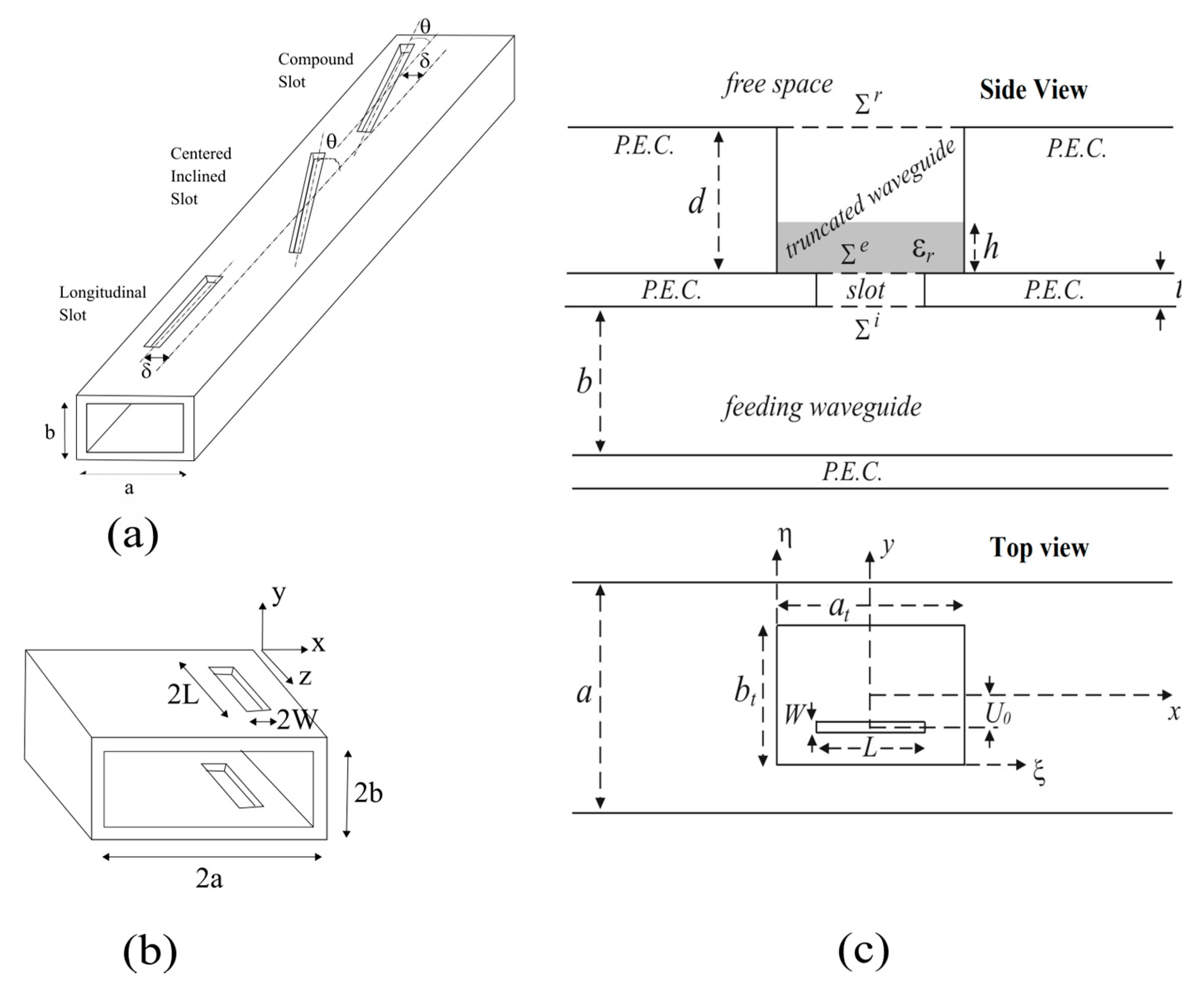
Figure 1. Waveguide slot models: (a) Typical broad-wall radiating slots; (b) slot doublet; and (c) waveguide longitudinal slot with cavity.
Electronics 10 01311 g001
Figure 2. Geometry of a typical planar waveguide slot array with longitudinal radiating slots. (a) 3D view. (b) Top view.
Electronics 10 01311 g002
Figure 3. Side view of waveguide slot arrays (WSAs) with waveguides partially filled with a dielectric slab. (a) “Comb-like” structure with copper-clad laminate as a “cover”. (b) “Comb-like” structure with a dielectric slab and slotted wall as a “cover”. (c) Array model used in the synthesis procedure.
Electronics 10 01311 g003
Figure 4. (a) Simulated far-field pattern requiring a Taylor nominal pattern and having a sidelobe level SLL = −20 dB (E-plane) for (i) an array having a common dielectric layer and (ii) an array approximate model considering separate radiating waveguides. (b) Simulated far-field pattern requiring nominal uniform distribution (H-plane) for (i) an array having a common dielectric layer and (ii) an array approximate model considering separate radiating waveguides. (c) Frequency response for (i) an array having a common dielectric layer and (ii) an array approximate model considering separate radiating waveguides.
Electronics 10 01311 g004
Figure 5. 3D view of a WSA with the radiating waveguides covered by a dielectric layer.
Electronics 10 01311 g005
Figure 6. (a) Far-field pattern simulated with HFSS in the H-plane, with a nominal Chebychev pattern with −30 dB sidelobes. The continuous line refers to “dielectric coupling”, while the dashed line refers to “free space coupling”. (b) Far-field pattern simulated with HFSS in the E-plane with a nominal uniform pattern. The continuous line refers to “dielectric coupling”, while the dashed line refers to “free space coupling”. The cross-polar components are not reported because their level was below −45 dB. (c) Frequency response simulated with HFSS. The continuous line refers to “dielectric coupling”, while the dashed line refers to “free space coupling”.
Electronics 10 01311 g006aElectronics 10 01311 g006b
Figure 7. Radiating slot geometry in a waveguide with a multilayer dielectric cover using four dielectric layers. (a) Top view. (b) Side view.
Electronics 10 01311 g007
Figure 8. Three-layer case. The continuous lines represent the resonant length of the slot with respect to the thickness h1 of the first covering layer. The dashed lines represent the conductance at resonance, normalized to the waveguide fundamental mode admittance with respect to the thickness h1 of the first covering layer. Frequency = 9 GHz.
Electronics 10 01311 g008
Figure 9. Three-layer case. The continuous lines represent the resonant length of the slot with respect to the thickness h2 of the second covering layer. The dashed lines represent the conductance at resonance, normalized to the waveguide fundamental mode admittance with respect to the thickness h2 of the second covering layer. Frequency = 9 GHz.
Electronics 10 01311 g009
Figure 10. Geometry of the analyzed array. (a) Side view. (b) Top view.
Electronics 10 01311 g010
Figure 11. Gain of an array with 6 × 6 elements and a dielectric cover and of an array with 8 × 8 elements radiating in free space (HFSS simulations). (a) E-plane. (b) H-plane. (c) Simulated frequency responses of the 6 × 6 and 8 × 8 designed arrays using HFSS.
Electronics 10 01311 g011
Figure 12. Gain of an array with 8 × 8 elements and a dielectric cover and of an array with 10 × 10 elements radiating in free space (HFSS simulations). (a) E-plane. (b) H-plane. (c) Simulated frequency responses of the 8 × 8 and 10 × 10 designed arrays using HFSS.
Electronics 10 01311 g012aElectronics 10 01311 g012b
Figure 13. (a) Subarray fed by a T-junction (side view and top view). (b) Five-port circuital and matrix models of the T-junction.
Electronics 10 01311 g013
Figure 14. Geometry of the analyzed monopulse planar WSA.
Electronics 10 01311 g014
Figure 15. E-plane far-field pattern of the monopulse WSA. The short bend length is equal to 12.4 mm, and the analysis model with the T-junction was performed using a straight shorted termination for the feeding waveguides with an impedance of 200 Ω.
Electronics 10 01311 g015
Table 1. Pros and cons of waveguide slot arrays (WSAs).
Advantages of WSAsDrawbacks of WSAs
Low power dissipation and low lossesSmall, useful bandwidth (resonant antennas)
High mechanical strengthHigh realization cost
Massive realizationLow flexibility
Small sizeWeak reconfigurability
Easily unfoldable-
High power handling capability-
High radiation efficiency-
Table 2. Advantages of the proposed WSA configurations.
Advantages
WSA
Configuration
PressurizationThermal InsulationGain EnhancementAerodynamic PurposesFlexibility
Standard WSA-----
WSA with waveguides covered with dielectric slabYesYes-YesYes
WSA with waveguides partially filled with dielectric slabYes---Yes
WSA with multilayer dielectric coverYesYesYesYesYes
Table 3. Comparison of the state-of-the-art works, considering several WSAs with different configurations.
Ref.Freq
(GHz)
No. of ElementsAperture Size (λ02)RLBW
(−10 dB)
ARBW
(3 dB)
GBW
(3 dB)
PGηSLL
(dB)
[34]3010 × 10.9 × 64%8%4%16.3dBi98%−18.5
[47]1208 × 85.67 × 5.6713.3%-13.3%25 dBi75%−13
[48]28.64 × 94.3 × 8.67%-7%24.8 dBi75%−11.5
[62]304 × 43.5 × 3.540.21%36.51%37.02%19 dBic-−13
[63]294 × 410.25 × 8.729.6%25.4%19%20.3 dBic57.9%−10
[64]308 × 86.12 × 6.1227.6%32.7%30%25.2 dBic75.2%−13
[65]284 × 47 × 527.7%27.8%25.3%20.2 dBic78%−10
[69]288 × 87.6 × 7.628%-25.2%26.4 dBi60%−13
[70]6016 × 1615.4 × 15.611.4%-11%33.5 dBi83.6%−14.9
[71]128 × 87.4 × 7.436.9%-31.9%23.4 dBi60%−21.3
[72]608 × 87.6 × 6.930%-29.1%27.5 dBi80%-
[73]78.532 × 3229.56 × 29.5619%-19%38.4 dBi76.4%−13
[74]6216 × 167 × 6.416%-16%32.5 dBi70%−13
[75]13032 × 3230.43 × 30.4312%-12%38 dBi60%−13
[81] 98 × 85.92 × 7.82%-2%27.1 dBi67%−20
[84]9.364 × 2455.8 × 174.3%-4.3%37.7 dBi50%−22.5
[85]3522 × 122.68.57 × 2.923.7%3.7%3.7%23.3 dBic75%−28
[86]9416 × 1617.23 × 17.2321%-21%30.5 dBi60%−20
[87]4022 × 2017.23 × 17.233.75%-3.75%31.8 dBi-−30
RLBW: return loss bandwidth; ARBW: axial ratio bandwidth; GBW: gain bandwidth; PG: peak gain; and η: efficiency.
Publisher’s Note: MDPI stays neutral with regard to jurisdictional claims in published maps and institutional affiliations.