Article

Parameter Estimation of a Single-Phase Boost PFC Converter with EMI Filter Based on an Optimization Algorithm

by
Gabriel Rojas-Dueñas
1,
Jordi-Roger Riba
1 and
Manuel Moreno-Eguilaz
2,*
1
Electrical Engineering Department, Universitat Politècnica de Catalunya, Rambla Sant Nebridi 22, 08222 Terrassa, Spain
2
Electronics Engineering Department, Universitat Politècnica de Catalunya, Rambla Sant Nebridi 22, 08222 Terrassa, Spain
*
Author to whom correspondence should be addressed.
Electronics 2021, 10(11), 1231; https://doi.org/10.3390/electronics10111231
Submission received: 20 April 2021 / Revised: 12 May 2021 / Accepted: 19 May 2021 / Published: 21 May 2021
(This article belongs to the Special Issue Digital Control in Power Electronics)

Abstract

:
This paper proposes an approach to estimate the parameters of an AC–DC boost power factor corrector converter that includes an EMI filter. To this end, once the topology was known, the values of the passive elements were identified from measurements at the input and output terminals of the converter. The parameters of the converter were identified based on the trust region nonlinear least squares algorithm. The steady-state and the transient signals of the converter at the input/output terminals were acquired non-intrusively without any internal modification of the circuitry. The accuracy of the proposed parameter identification approach was determined by comparing the estimated values with those provided by the manufacturer, and by comparing the measured signals with those obtained with a simulation model that included the estimated values of the parameters. The results presented in this paper prove the accuracy of the proposed approach, which can be extended to other power converters and filters.

1. Introduction

Power factor corrector (PFC) converters are devices designed to improve the power quality of a distribution system by improving the power factor and reducing the total harmonic distortion (THD) [1,2]. They are mainly used in applications involving a large number of electronic loads, which generate harmonic currents and inject reactive power to the electrical system [3]. In these scenarios, the use of PFC converters is necessary in order to fulfill the requirements of international power quality standards, such as the IEEE Std. 519 [4]. Boost PFCs are widely used in household appliances, laptop adapters, on-board chargers, or in aircraft power supplies, among other devices [5]. When using switching-mode power converters such as the boost PFC, it is required to add an electromagnetic interference (EMI) filter at the input terminals in order to attenuate the conducted EMI disturbances generated by the electronic equipment toward the power line [6] and fulfill the stringent requirements of EMI-related international standards. Companies of the aforementioned sectors typically integrate boost PFCs and EMI filters in systems that include many other power devices and components from different manufacturers. These companies need accurate models of the devices to perform several tasks, such as the design of controllers, the application of predictive maintenance approaches, or calculation of the energy consumption, among others [7]. However, manufacturers of power devices often do not provide enough information regarding the topology or characteristics of internal components due to confidentiality reasons [8]. During the design and optimization stages of the development of power electronics devices, engineers require the values or parameters of their constitutive components in advance to generate accurate discrete models [9]. Therefore, it is highly appealing to develop a method to estimate these values in order to develop models to replicate the behavior of power electronics devices with high accuracy.
To our knowledge, there have been no studies dealing with the topic of parameter identification of boost PFCs including an input EMI filter. However, the literature includes different approaches for identifying the parameters of switched-mode power converters, such as buck, boost, or buck–boost converters. In [10,11], the authors proposed an estimation method based on obtaining state space averaging models of the converters, where the converter topology was used to obtain a transfer function that was tuned using measured data. In [7], the parameters of a buck and a boost converter were identified by calculating the analytical equations describing the behavior of the circuits, although this an intrusive approach because it requires measuring the current in the inductor. Ahmeid et al. [12], by using a Kalman filter, estimated in real time the transfer function of a synchronous buck converter. In [13], the dichotomous coordinate descent method was applied for an online identification of the voltage transfer function of a DC–DC converter, although an external excitation was required. In [14], the passive and parasitic elements of DC–DC converters were calculated by means of a continuous time model that applies a polynomial interpolation. In [15], a buck converter was modeled by means of a NARX neural network. However, the parameters were not identified since it generates a black-box model. In [16], a parameter estimation of buck, boost and buck–boost converters was carried out by applying an optimization algorithm that identifies the values of the passive elements. The authors in [17] presented a review of the state-of-the-art of parameter identification methods for DC–DC power converters, although despite the accurate results, all reviewed approaches are invasive or intrusive since they require external excitations or internal measurements.
The technical literature reveals that most of the works related to EMI filters identify the filter from a simplified transfer function [18] or perform an electromagnetic analysis of the filter components [19,20]. Thus, they do not provide the actual values of the filter parameters. There is an imperious need to non-intrusively identify simultaneously all parameters of the electronic device from the input/output voltages/currents because the input/output terminals are often the only accessible points.
This paper proposes identifying all parameters of a boost PFC converter that includes an EMI filter stage. It is based on an optimization algorithm that requires non-intrusive measurements from the input and output terminals of the converter and the filter. A methodology that comprises four optimization stages based on the trust region nonlinear least squares algorithm is also proposed. This paper demonstrates that it is possible to simulate the behavior of the PFC converter with high fidelity once the values of the parameters have been identified. The proposed approach is able to estimate more than 30 parameters based on measurements at the input and output terminals of the different PFC converter elements, which is advantageous because manufacturers often do not disclose information about the inner components of devices. This identification procedure represents a more realistic way of modeling the converter than methods based on transfer functions. It can be applied to tasks such as planning, prognosis, or energy management, among others. The main novelties and contributions of the paper are found in Section 5.

2. The AC–DC Power Factor Correction Converter

The boost PFC analyzed in this paper is an AC–DC converter used to obtain an output DC voltage from an AC source with a high power factor [21]. This converter is widely used in many industry applications because it can supply multiple loads while continuously regulating the output voltage [22]. The boost PFC is a switched-mode power converter (SMPC) that applies a pulse width modulation (PWM) strategy to efficiently convert the electrical power. A side effect of this conversion is the generation of high-frequency switching harmonics, which induce parasitic effects on the different elements of the circuit. It also induces electromagnetic interference (EMI), which is a disturbance affecting electric and electronic circuit via conduction, electromagnetic induction, or electrostatic coupling, tending to degrade the behavior of the circuit. To mitigate this interference and to fulfill the requirements of EMI standards, an EMI filtering stage is required at the input of the boost PFC converter.
Figure 1 shows the block diagram of the power converter to be identified in this paper. It is divided in four different stages, each one including different physical and non-physical parameters to be identified. These four stages are the EMI filter, the single-phase AC–DC rectifier, the DC–DC boost converter, and the control loop of the SMPC converter.
The topologies of the EMI filter and the boost PFC converter are based on commercially available components. The first one is the 10VN1 power line filter model, manufactured by Corcom (Libertyville, USA). This EMI/RFI filter is used between the power line and the electronic equipment to attenuate the conducted EMI disturbances generated by the electronic equipment toward the power line [6]. It is designed for providing differential- and common-mode attenuation for digital equipment, such as switching power supplies, over the 10 kHz to 30 MHz frequency range. Figure 2 shows the circuit of the EMI filter used at the input stage of the boost PFC. The circuit includes 12 parameters to be identified, which correspond to the passive elements of the circuit. Commonly, the values of the coupled inductors (L1 and L2) and the capacitors with common ground (C3 and C4) are identical, thus reducing the number of parameters to be estimated and simplifying the identification process.
The AC–DC boost PFC converter consists of a single-phase rectifier connected to a step-up high-frequency switching DC–DC converter that is regulated by means of two control loops (voltage and current). The boost PFC converter studied in this paper is the ISA102V2 evaluation module manufactured by ST, which is an 80 W high performance transition mode PFC board based on the L6562A controller. The AC–DC conversion is done by means of a full wave diode bridge with an output smoothing capacitor. The rectifier feeds a classic boost converter. Due to the high-switching frequencies of the transistors, it is important to consider the parasitic resistance of the capacitor and the inductor.
Figure 3 presents the circuit of the boost PFC and the elements whose values must be identified. The exponential model of the diode was used since it reproduces accurately its behavior [23] by relating the current flowing across the diode to its voltage drop as,
I = I s × ( e q V / ( N k T m ) 1 )
where I and Is refer to the diode current and saturation current, respectively, V is the voltage drop across the terminals of the diode, q is the elementary charge of an electron, k is the Boltzmann constant and Tm is the working temperature.
The controller of the DC–DC converter has two main objectives. The first one is to maintain a power factor close to 1 by using an inner current control loop, so the input voltages and currents should be almost in phase. The second objective is to deliver a constant output voltage by means of an outer voltage control loop [24]. It regulates the output voltage to a given reference value. Both loops apply a PI compensation, thus creating a robust control scheme of the boost PFC converter.
Figure 4 presents the block diagram of the controller along with the implementation of its circuitry. The current control is a PI compensation because it is normally implemented in the microcontroller unit of the converter and it can be modeled as a transfer function. Figure 4 indicates that the reference value of the inductor current is given by the output generated by the outer voltage loop. The compensation of the outer voltage control loop is performed by a type 3 operational amplifier, as shown in Figure 4b. This type of compensation provides two poles and two zeros being used when a phase boost greater than 90 degrees is needed [25]. The reference voltage is specified by the designer and the values of the resistors and capacitors must be identified.
Given the topologies of the four blocks presented in this section, there are 33 unknown values to be estimated. They correspond to the parameters of the EMI filter (R,C1,C2,C3,C4,C5,C6,L1,L2,L3,L4,L5), the single phase rectifier (IS,N,Tm,Rdiode,Csmooth), the boost converter ( C , R C , L , R L , R S 1 , R S 2 ) , and the control loops ( R 1 , R 2 , R 3 , R 4 , R 5 , C 1 , C 2 , C 3 , K P , K I ). The following sections present the proposed methodology to identify these parameters and the data acquisition procedure.

3. The Proposed Parameter Estimation Methodology

This section presents the proposed approach to identify the parameters of the boost PFC converter. First, it introduces the main core of the parameter identification strategy, which is the nonlinear least squares (NLS) optimization algorithm. Next, the proposed methodology is described.

3.1. Nonlinear Least Squares Optimization for Parameter Estimation

This section presents the algorithm used in this paper to estimate the parameters of the boost PFC converter. It is well known that switched-mode power converters, as the one analyzed in this paper, have nonlinear characteristics, preventing conventional parameter estimation methods of obtaining accurate results [26]. Thus, the trust region reflective least squares algorithm is used because it is able to deal with nonlinearities. It is mainly used to tune parameters of constrained nonlinear problems. The algorithm finds a set of variables x with the purpose of minimizing an objective function [27] given by:
min x E ( X ) = min x ( i = 1 n e i 2 ( x ) )
where ei(x) refers to the error function, which is defined according to the type of problem. It is constrained by the lower and upper bounds of the variables in the form of lbxub [16]. The optimization approach aims to replicate the behavior of e(x) in a neighborhood N (trust region) by means of a quadratic function q(s) [28]. The main purpose of this algorithm is to expand the Taylor series of q(s) and to obtain the trust region of the problem. The region N is generated around the actual value of xk and, consequently, the main challenge of the iterative process is to find the xk+1 point within the N neighborhood. The selection of the new point must satisfy e(xk+1) < e(xk), otherwise the trust region N is reduced, and the point xk does not change. Therefore, a proper selection of the iteration step Sk = xk+1xk is needed, which is obtained by solving the subproblem,
min s N q k ( s ) = min s N ( g ( x ) T s + 1 2 s T H ( x ) s )
where g(x) and H(x) correspond to the gradient and the Hessian matrix of e(x) evaluated in x k , respectively. The condition s N can be expressed in the form of || D k 1 s || < Δ i , D being the diagonal scaling matrix and Δ i the size of the trust-region. D is calculated by means of a vector function, which is defined by v ( x ) = [ v 1 ( x ) , v 2 ( x ) , , v n ( x )   ] T and it is obtained according to the gradient of the error function, the boundaries (ub and lb), and the actual state x k [16]. Thus, for a given x k , the value of sk is calculated by using (3) and x k + 1 = x k + α k s k , where α k represents the step length. This length merely depends on the interior of N (int(N)), which is defined by the upper and lower bounds of the variables being optimized. The iterative process carried out to find the minimum value of e(x) is based on the reflective line search (RLS), which determines how the iterations move over the boundary of int(N). To accelerate the convergence of the optimization process, the space int(N) is limited to a subspace V of two dimensions. This restriction enhances the speed of the algorithm because the mathematical calculations of the eigenvectors and eigenvalues are easier due to the lower dimension of the subspace [29]. By using a 2D subspace, the problem can be solved with well-known and less complex algorithms such as the preconditioned conjugate gradient method. Furthermore, the Jacobian matrix J(x) approximates the Hessian matrix H(x), which is calculated by means of the efficient finite differencing method [28]. The initial or seed point defined prior to the optimization process plays an important role in the trust region reflective algorithm since it determines the step length and how the trust region reduces after each iteration. Therefore, the local minimum reached after the NLS optimization is conditioned by the initial value of x 0 .
Considering the characteristics of the boost PFC converter mentioned in the previous subsection, and the data that can be retrieved from it, the objective function of the parameter identification problem is defined as follows:
min x ( i = 1 n ( [ V i n e s t ( t ) V i n m e a s ( t ) ] 2 + [ I i n e s t ( t ) I i n m e a s ( t ) ] 2 + [ V o u t e s t ( t ) V o u t m e a s ( t ) ] 2 + [ I o u t e s t ( t ) I o u t m e a s ( t ) ] 2 ) ) ,   t = i T
V and I refer, respectively, to the normalized values of the voltage and current, the subscripts denoting the port where the signals are obtained, the superscripts indicate whether the signal is estimated by the model or acquired in the laboratory, n represents the total number of time steps considered, T is the length of the time step, and t is the time instant where the error function is being evaluated. The variables x to be optimized are the values of the electrical elements of the EMI filter and boost PFC converter and the control parameters mentioned in Section 2. The minimum and maximum values of these variables define the trust region N of the NLS optimization. However, if all variables are identified simultaneously, N would be too large and the problem too complex to solve. The following subsection presents the proposed methodology to identify all the parameters.

3.2. Proposed Parameter Identification Methodology

Given the complexity of the circuit and the large number of variables to be identified, it is necessary to define a methodology to identify all the parameters with high accuracy and a reduced simulation time. The simultaneous identification of all parameters may lead to an incorrect solution because it is very likely that the optimization approach finds a local minimum, thus the solution would differ from the actual parameters of the converter.
Figure 5 shows the proposed algorithm, which aims to separately identify certain sets of parameters in order to reduce uncertainty and obtain better results.
The algorithm is divided into four steps, which correspond to the four blocks of the diagram shown in Figure 1 (EMI filter, rectifier, boost converter, and controller). The first step of the methodology consists of defining the topology of all components and to specify the variables to be estimated. This was done in Section 2. The next step is to identify the values of the EMI filter parameters and the rectifier, these being independent processes that can run in parallel. The third stage estimates the open loop parameters of the boost converter using the previously identified values and topologies of the EMI filter and rectifier. Finally, the control or closed loop parameters of the converter are estimated using the NLS algorithm. A thorough explanation of each optimization stage is given as follows:
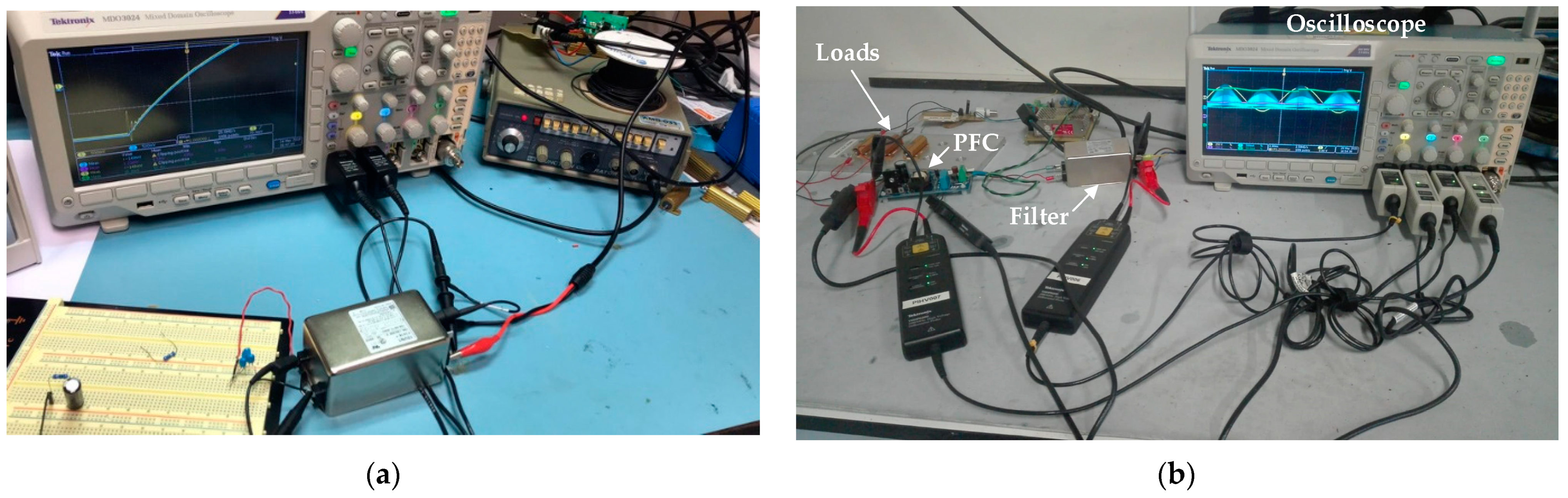
  • EMI filter: This stage aims to identify the 12 values of the passive elements of the EMI filter. First, the experimental setup and the data to be acquired in the laboratory are defined. To force a sufficient rich response of the EMI filter that enables identifying the values of the parameters, a capacitor was connected at the output terminals in parallel with the resistive load while applying a periodic square waveform voltage to the input terminals. To perform the identification process, the voltage and current at the input and output terminals are needed. To simulate the high output impedance of the function generator used to generate the square waveform, a resistance Rin in series with an inductance Lin were added to the Simulink® model, and the values of such parameters were identified jointly with the parameters of the filter. To enhance the performance of the identification process, the data were divided into two sets, which were used in the optimization process, i.e., the data centered in the rising and in the falling edges of the periodic square waveform. This is done to focus on the intervals that contain the relevant information. Figure 6 shows the Simulink® model used to identify the parameters of the passive EMI filter.
  • Rectifier: The identification process of the parameters of the single-phase rectifier is independent of the other elements of the boost PFC converter since it just uses the acquired signals at the input and output terminals of the rectifier. This process aims to estimate the diode and the output capacitor parameters. The complexity of this stage depends on the considered diode model, the exponential in this case, as described by (1).
    In order to obtain an accurate representation of the exponential model, the parameter estimation method uses the data acquired in three experiments of the rectifier, in which the load connected at the output terminals was changed. The NLS optimization algorithm identifies the values of the parameters by fitting the curves of three operating points of the rectifier. Figure 7 shows the corresponding Simulink model.
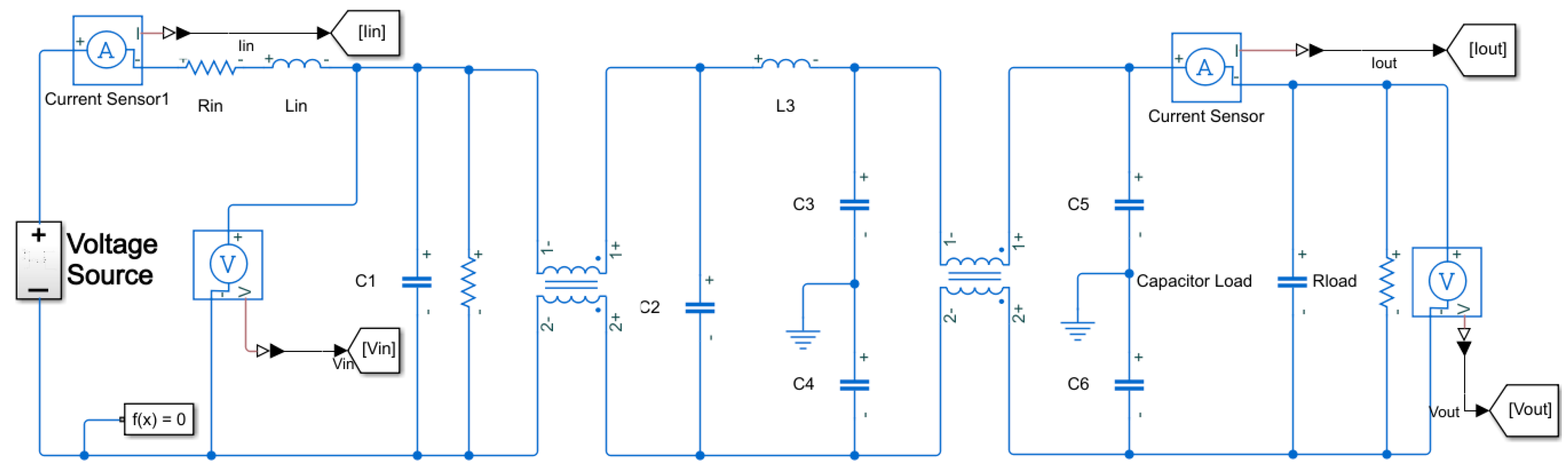
  • Boost converter (open loop): The third stage of the proposed methodology is the estimation of the values of the boost converter electrical components. The available data are the currents and voltages at the input terminals of the EMI filter and at the output of the boost converter. Therefore, the previously estimated parameters of the EMI filter and the rectifier are required in this optimization process. As explained in Section 2, the parasitic components are also considered in order to obtain accurate results.
    The data used in this stage are based on the steady state behavior of the converter when it is connected to a certain load. The timespan of the acquired signals is chosen as a tradeoff between the simulation speed and the accuracy. Thus, the parameters can be estimated by analyzing two or three periods of the measured signals. The corresponding Simulink model is shown in Figure 8.
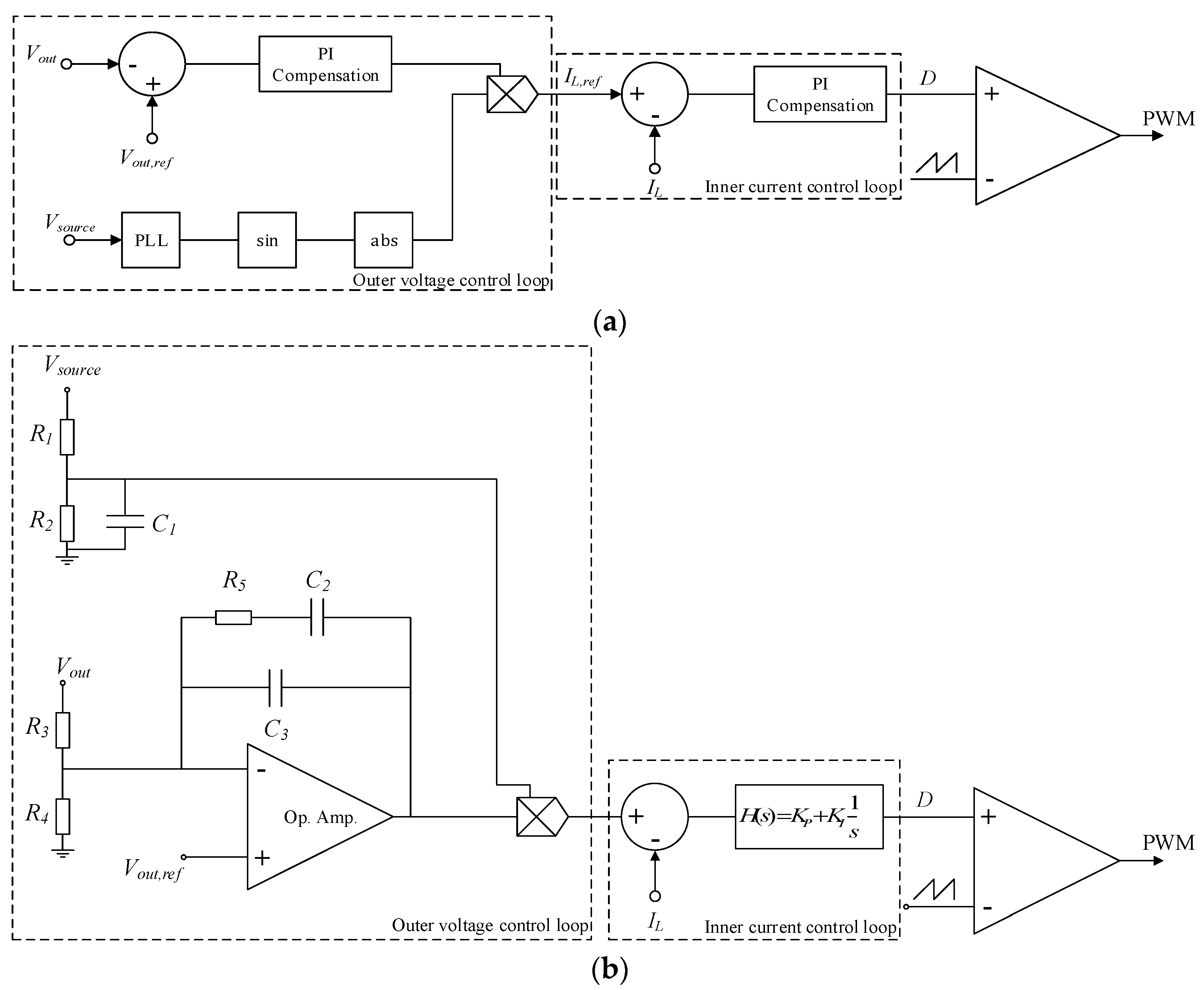
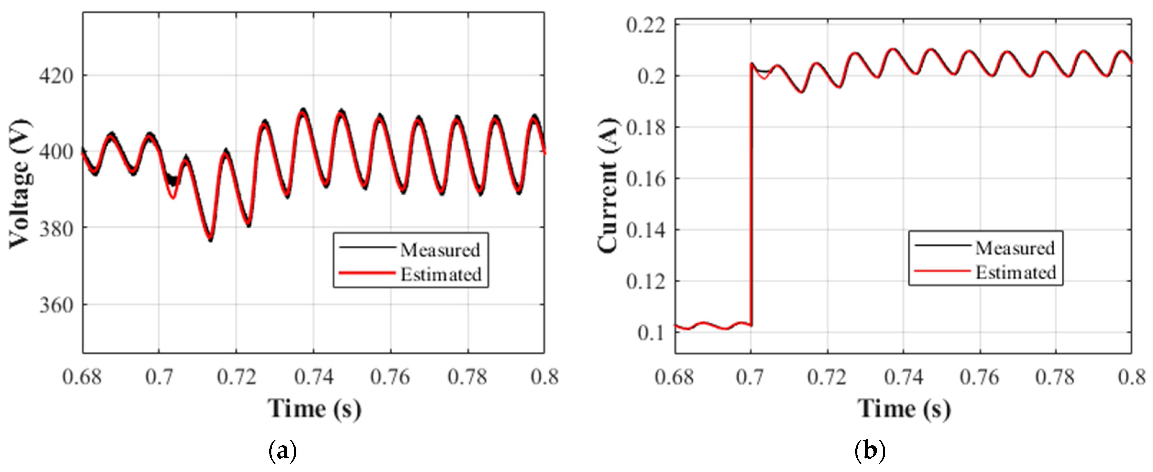
  • Control parameters (closed loop): The last stage identifies the values of the boost PFC control loop parameters listed in Section 2. It also re-estimates the value of the capacitor of the converter because it affects the transient response of the outer voltage loop [24]. It uses the values estimated in the previous stages and adds the voltage and current control loops to the Simulink model. The experimental setup is the same as in the open loop identification stage. However, the converter is subjected to a load change at the output terminal to obtain its transient response. The timespan of the data acquired is chosen depending on the time that the converter requires to reach the steady state. In this stage, the NLS algorithm requires more time compared to the other stages because it uses a model with a higher complexity and a larger dataset. Figure 9 shows the corresponding Simulink model of the control loop that was added to the boost PFC presented in Figure 8.
As shown in Figure 5, each stage of the proposed algorithm includes a data pre-processing step, which is fundamental to the optimization process. This step consists of re-sizing, filtering, and synchronizing the raw data according to the data generated by the Simulink models. The resizing step consists of reducing the number of measured data points without losing relevant information. It is done by means of an interpolation, directly affecting the computational burden of the process. Once the data is re-sized, the next step is to eliminate the high-frequency noise by applying a low-pass finite impulse response filter as it is the moving average. Finally, the time vector of the measured signals is modified to synchronize the data generated from the simulations with the experimental data, which is essential for curve-fitting purposes.
Another important aspect to consider is the definition of the seed point and the upper and lower boundaries of the parameters to be identified. The selection of the initial point is based on a priori knowledge of the different elements of boost PFC converters, and the boundaries are set to cover six orders of magnitude, i.e., a typical initial value of the inductor in a boost converter is 1 µH so that the lower and upper boundaries are set to 1 nH and 1 mH, respectively.
After each NLS optimization iteration, the error value is compared to a fixed value δ that is selected at each stage of the proposed algorithm. This value is set to 0.01 for all stages. If the error value is higher than the defined threshold, the initial point and the constraints are modified by multiplying the obtained values by a random number between 0.75 and 1.25 and the NLS optimization starts again. This is done to ensure that the process reaches a different local minimum than the last one. The algorithm advances to the next step when the error value is lower than δ, otherwise it iterates. Equation (5) defines the error, which is calculated based on the experimental and estimated values of the signals used in the optimization process.
e r r o r = i = 1 S i g M e a n ( | x i , n o r m , e x p x i , n o r m , e s t x i , n o r m , e x p | )
In this equation, x refers the signals that are fitted in the NLS optimization process. Their values are normalized to have the voltages and currents of similar magnitudes for a proper comparison.

4. Results

This section presents the experimental results obtained with the EMI filter and the boost PFC converter. For this purpose, the input and output voltages and currents were acquired under the conditions specified in the previous section.
As mentioned in Section 2, the EMI filter and boost PFC used in the laboratory in the parameter estimation process are the Corcom 10VN1 and the STMicroelectronics STEVAL-ISA102V2, respectively. The maximum rated voltage of the filter is 250 VAC, its rated current is in the range 6–10 A, and the operating frequency could be 50 Hz or 60 Hz. The specifications of the boost PFC are listed in Table 1.
The equipment used to measure the voltages and currents of the different devices consisted of a four-channel oscilloscope (Tektronix MDO3024 200 MHz 2.5 GS/s; Tektronix, Beaverton, OR, USA), two high-frequency current probes (Tektronix TCP0030A 0.001-20 A 120 MHz; Tektronix, Beaverton, OR, USA), and two high-frequency differential probes (Tektronix THDP200; Tektronix, Beaverton, OR, USA).
Figure 10 presents the experimental setup used to acquire the necessary data in the parameter estimation process. Figure 10a shows the setup used in the EMI filter identification stage of the proposed methodology, while the experimental setup presented in Figure 10b was used for the identification of the other stages of the methodology.

4.1. EMI Filter Parameter Identification

According to the methodology presented in Figure 5, the parameter identification of the EMI filter is the first stage of the process. To this end, the data was acquired according to the procedure explained in Section 3.2. The periodic square wave voltage applied to the filter had an amplitude of 2 V and a frequency of 50 Hz, while the load consisted of an 11 µF capacitor connected in parallel to an 11 Ω resistor. Table 2 presents the lower and upper bounds as well as the values of the parameters identified by the NLS optimization algorithm. It also shows the values given by the manufacturer. The simulation time was about 8 h and 42 min using an Intel® Xeon® CPU, ES.1650 v2 3.50 GHz, with 64 GB of RAM memory.
Figure 11 and Figure 12 show the experimental and estimated signals at the input and output terminals of the EMI filter, as well as the magnitude and phase Bode plots of the filter. The estimation was done by simulating the electrical model of Figure 2 using the identified parameters presented in Table 2. The results show a good agreement between experimental and simulated results considering the identified parameters, and the frequency response is almost the same for both cases.

4.2. Rectifier Parameter Identification

Since the single-phase rectifier was integrated in the evaluation module of the boost PFC used in this paper, the data acquired in this stage was based on the experimental setup presented in Figure 10b. However, the EMI filter was not used and the voltage and current probes were placed at the input of the boost PFC and at the smooth capacitor. The rectifier was fed at 230 V and 50 Hz. As mentioned in Section 3.2, the rectifier must be tested under different operating points due to the requirements of the exponential diode model, so the output loads were selected to 3.9 kΩ, 1.95 kΩ, and 7.8 kΩ. The simulation time was about 1 h and 7 min, which is relatively fast considering the type of problem.
Table 3 presents the main values of the NLS optimization procedure and compares the optimal point to the actual values of the rectifier. It is important to mention that some parameter values were not provided by the manufacturer.
Since the theoretical values of the rectifier parameters were unknown, Figure 13 compares the measured values of the output voltage and current with the estimated ones. These results show that the estimation reproduced with high fidelity the amplitude, mean value, and frequency of the output signals of the single-phase rectifier. Figure 13c shows that the high-frequency switching characteristics of the output current were also replicated with accuracy. Figure 14 shows the estimation of the forward I–V curve of the diode, which was calculated using the identified parameters, and it is compared against the forward I–V curve provided by the manufacturer.

4.3. Boost Converter Parameter Identification

After identifying the parameters of the input filter and the AC–DC rectifier, the next stage of the proposed methodology is the identification of the steady state parameters of the boost PFC converter. The procedure explained in Section 3.2 was carried out and the data was measured using the setup presented in Figure 10b. A load of 3.9 kΩ was connected to the output of the converter and the timespan of the measurements was equivalent to three times the switching period of the boost converter. The duty cycle value was fixed to 0.12 because the control loop was not considered at this stage.
Table 4 presents the values of the initial point and boundaries of the parameters to be identified, as well as the comparison between the estimated and actual values of the passive elements. The simulation lasted for about 2 h and 56 min.
Results presented in Table 4 show a high accuracy in the identification of the parameters of the boost converter except for the capacitor. However, as already mentioned, this parameter also affects the transient behavior of the converter, so it is re-identified in the next stage of the process.
Figure 15 presents the measurements and steady-state estimation of the input and output signals of the converter. The estimated curves fit the acquired data with high precision and the ripple of the signals was the same.

4.4. Control Loop Parameter Identification

The last stage of the identification procedure consists of finding the parameters related to the outer voltage and inner current control loops. To estimate the parameters of the controller, it uses the models and identified values from the EMI filter, the rectifier, and the boost converter. The experimental setup presented in Figure 10b was used to acquire the data. A sudden load change was applied to capture the transient response of the boost PFC. The output load of the converter changed from 3.9 kΩ to 1.95 kΩ and the timespan of the measurements was defined according to the time that the converter needed to reach the steady state. As mentioned in the previous subsection, the value of the boost converter capacitor is also identified in this stage, its initial value being the estimated value obtained in the previous stage.
Table 5 shows the initial, minimum, maximum, estimated, and theoretical values of the controller parameters. The actual values of the proportional and integral constants are not specified because they were not given by the manufacturer. The time required in this optimization was 7 h and 46 min.
Results in Table 5 show that the identified value of the boost PFC capacitor was more accurate than the estimation done in the previous stage, while the values of the outer voltage control loop were identified with high precision.
Figure 16 compares the measured and estimated curves when a load change occurred. It can be observed that the simulation signals obtained with the identified parameters replicate the behavior of the boost PFC converter with accuracy.
The average relative error of the estimated parameters was 4.473%, which was calculated based on the error values presented in Table 2, Table 3, Table 4 and Table 5. Finally, the error of the fitting process was 0.00082, which was calculated by applying Equation (5) to the signals displayed in Figure 16a,b. Note that this value is more than ten times below the defined threshold δ = 0.01 .

5. Discussion

This work has contributed to the cutting edge of electronics in several aspects. First, it has proposed a strategy to estimate more than 30 parameters based on non-intrusive measurements at the input and output terminals of the different elements of the PFC converter. Second, the different elements of the control loops (voltage and current) were identified, which allows one to reproduce with high accuracy the transient behavior of the converter. Third, estimating all the parameters of a widely used device, such as an AC–DC PFC, can be advantageous in the design and maintenance of systems supplying multiple electronics loads. Fourth, the proposed algorithm is also capable of identifying the values of the parasitic components of the converter, which is useful for high-frequency switching devices as the one studied in this paper. Finally, the experimental setup to perform the data acquisition has been detailed and is relatively simple because it is not necessary to apply internal excitations to the circuit or perform invasive measurements in the inductor of the boost converter.
As mentioned in Section 1, there is a clear lack of literature related to the parameter identification of an AC–DC boost PFC converter with an EMI filter. Therefore, it is not possible to compare the proposed methodology with an existing approach. However, there are studies that identify the parameters of simple DC–DC converters, so only the parameters of the switched-mode power converter of the PFC device can be compared. The results obtained in the previous section were compared to the technique used in [7], which estimates the parameters of the boost converter by discretizing the differential equations governing its behavior. The average relative error resulting from calculating six parameters of the PFC DC–DC boost converter using the method presented in [7] is 7.44%, while the approach proposed in this paper identifies 33 parameters with an average error of 4.47%. This proves the accuracy of the methodology presented in this study.
One of the main causes of error in the parameter estimation process is the data acquisition uncertainty, which is the consequence of measuring at a high frequency rate. This can be improved by using an oscilloscope with higher resolution to measure the converter currents and voltages. To minimize the error, it is also convenient to reduce the space of possible solutions by defining a strategy to define the lower and upper boundaries of the variables to be estimated. Finally, it is necessary to consider the uncertainty of the values of the parameters provided by the manufacturer because it affects the calculation of the relative error.

6. Conclusions

Accurate modeling of power factor corrector converters is very important in applications involving a large number of electronic loads, which generate harmonic currents and inject reactive power to the electrical system. An accurate modeling may lead to improved designs, implementation of better control strategies, or fulfillment of industry standards, among many other advantages. This paper has presented a parameter identification strategy of a boost PFC converter integrating an EMI filter at the input stage. This approach uses the trust region nonlinear least squares optimization algorithm, the topology of the circuits, and non-intrusive measurements at the input and output terminals of the device. More than 30 parameters were identified with high precision and the behavior of the AC–DC converter was replicated with high accuracy. The experimental results show that the average relative error of the identified parameters was below 5%, which proves the accuracy of the proposed approach. This methodology can be applied to other power electronics devices.

Author Contributions

Conceptualization, M.M.-E. and G.R.-D.; methodology, J.-R.R.; formal analysis, M.M.-E. and J.-R.R.; investigation, J.-R.R. and G.R.-D.; writing—original draft preparation, G.R.-D. and J.-R.R.; writing—review and editing, M.M.-E. and G.R.-D. All authors have read and agreed to the published version of the manuscript.

Funding

This research was funded by the Generalitat de Catalunya, grant number SGR 2017 SGR 967 and the European Commission through the Clean Sky program, grant number 755332-AEMS-IdFit.

Conflicts of Interest

The authors declare no conflict of interest.

References

  1. Bodetto, M.; Aroudi, A.E.; Cid-Pastor, A.; Calvente, J.; Martínez-Salamero, L. Design of AC-DC PFC high-order converters with regulated output current for low-power applications. IEEE Trans. Power Electron. 2016, 31, 2012–2025. [Google Scholar] [CrossRef]
  2. Ren, X.; Wu, Y.; Guo, Z.; Zhang, Z.; Chen, Q. An Online Monitoring Method of Circuit Parameters for Variable On-Time Control in CRM Boost PFC Converters. IEEE Trans. Power Electron. 2019, 34, 1786–1797. [Google Scholar] [CrossRef]
  3. Bayona, J.; Gélvez, N.; Espitia, H. Design, Analysis, and Implementation of an Equalizer Circuit for the Elimination of Voltage Imbalance in a Half-Bridge Boost Converter with Power Factor Correction. Electronics 2020, 9, 2171. [Google Scholar] [CrossRef]
  4. Bao, J.; Liu, J.; Huang, Z.; Liu, W.; Li, H. An Online Parameter Identification for Ultracapacitor Model by Using Recursive Least Square with Multi-forgetting Factor. In Proceedings of the 2018 13th World Congress on Intelligent Control and Automation (WCICA), Changsha, China, 4–8 July 2018; pp. 962–966. [Google Scholar]
  5. Xu, H.; Chen, D.; Xue, F.; Li, X. Optimal design method of interleaved boost PFC for improving efficiency from switching frequency, boost inductor, and output voltage. IEEE Trans. Power Electron. 2019, 34, 6088–6107. [Google Scholar] [CrossRef]
  6. Kotny, J.-L.; Margueron, X.; Idir, N. High-Frequency Model of the Coupled Inductors Used in EMI Filters. IEEE Trans. Power Electron. 2012, 27, 2805–2812. [Google Scholar] [CrossRef]
  7. Riba, J.; Moreno-eguilaz, M.; Bogarra, S.; Garcia, A. Parameter Identification of DC-DC Converters under Steady-State and Transient Conditions Based on White-Box Models. Electronics 2018, 7, 393. [Google Scholar] [CrossRef] [Green Version]
  8. Valdivia, V. Behavioral Modeling and Identification of Power Electronics Converters and Subsystems Based on Transient Response; Universidad Carlos III de Madrid: Madrid, Spain, 2013. [Google Scholar]
  9. Oliver, J.A.; Prieto, R.; Romero, V.; Cobos, J.A. Behavioural Modelling of DC-DC Converters for Large-Signal Simulation of Distributed Power Systems. In Proceedings of the Twenty-First Annual IEEE Applied Power Electronics Conference and Exposition, 2006. APEC’06., Dallas, TX, USA, 18 April 2006. [Google Scholar] [CrossRef]
  10. Wang, L.; Deng, X.; Han, P.; Qi, X.; Wu, X.; Li, M.; Xu, H. Electromagnetic Transient Modeling and Simulation of Power Converters Based on a Piecewise Generalized State Space Averaging Method. IEEE Access 2019, 7, 12241–12251. [Google Scholar] [CrossRef]
  11. Nabinejad, A.; Rajaei, A.; Mardaneh, M. A Systematic Approach to Extract State-Space Averaged Equations and Small-Signal Model of Partial-Power Converters. IEEE J. Emerg. Sel. Top. Power Electron. 2020, 8, 2475–2483. [Google Scholar] [CrossRef]
  12. Ahmeid, M.; Armstrong, M.; Gadoue, S.; Algreer, M.; Missailidis, P.; Al-Greer, M.; Missailidis, P. Real-Time Parameter Estimation of DC–DC Converters Using a Self-Tuned Kalman Filter. IEEE Trans. Power Electron. 2017, 32, 5666–5674. [Google Scholar] [CrossRef] [Green Version]
  13. Algreer, M.; Armstrong, M.; Giaouris, D. Active Online System Identification of Switch Mode DC–DC Power Converter Based on Efficient Recursive DCD-IIR Adaptive Filter. IEEE Trans. Power Electron. 2012, 27, 4425–4435. [Google Scholar] [CrossRef]
  14. Buiatti, G.M.; Amaral, A.M.R.; Cardoso, A.J.M. An unified method for estimating the parameters of non-isolated DC/DC converters using continuous time models. Telecommun. Energy Conf. 2007. INTELEC 2007. 29th Int. 2007, 334–341. [Google Scholar] [CrossRef]
  15. Rojas-Duenas, G.; Riba, J.-R.; Kahalerras, K.; Moreno-Eguilaz, M.; Kadechkar, A.; Gomez-Pau, A. Black-Box Modelling of a DC-DC Buck Converter Based on a Recurrent Neural Network. In Proceedings of the 2020 IEEE International Conference on Industrial Technology (ICIT), Buenos Aires, Argentina, 26–28 February 2020; Institute of Electrical and Electronics Engineers (IEEE): Buenos Aires, Argentina, 2020; pp. 456–461. [Google Scholar]
  16. Rojas-Dueñas, G.; Riba, J.-R.; Moreno-Eguilaz, M. Non-Linear Least Squares Optimization for Parametric Identification of DC-DC Converters. IEEE Trans. Power Electron. 2021, 36, 654–661. [Google Scholar] [CrossRef]
  17. Al-Greer, M.; Armstrong, M.; Ahmeid, M.; Giaouris, D. Advances on system identification techniques for DC-DC switch mode power converter applications. IEEE Trans. Power Electron. 2019, 34, 6973–6990. [Google Scholar] [CrossRef] [Green Version]
  18. Labarre, C.; Costa, F. Circuit analysis of an EMI filter for the prediction of its magnetic near-field emissions. IEEE Trans. Electromagn. Compat. 2012, 54, 290–298. [Google Scholar] [CrossRef]
  19. Wang, N.; Yan, Z.; Tang, J.; Ning, Z.; Xiao, B.; Wang, H. Study on Prediction Models of EMI Filter with Near-field Coupling Effect. In Proceedings of the 2018 12th International Symposium on Antennas, Propagation and EM Theory, ISAPE 2018—Proceedings, Hangzhou, China, 3–6 December 2018; Institute of Electrical and Electronics Engineers Inc.: New York, NY, USA, 2019. [Google Scholar]
  20. Narayanasamy, B.; Luo, F.; Chu, Y. Modeling and Stability Analysis of Voltage Sensing based Differential Mode Active EMI Filters for AC-DC Power Converters. In Proceedings of the 2018 IEEE Symposium on Electromagnetic Compatibility, Signal Integrity and Power Integrity, EMC, SI and PI 2018, Long Beach, CA, USA, 30 July–3 August 2018; Institute of Electrical and Electronics Engineers Inc.: New York, NY, USA, 2018. [Google Scholar]
  21. Zhang, R.; Ma, W.; Wang, L.; Hu, M.; Cao, L.; Zhou, H.; Zhang, Y. Line Frequency Instability of One-Cycle-Controlled Boost Power Factor Correction Converter. Electronics 2018, 7, 203. [Google Scholar] [CrossRef] [Green Version]
  22. Singh, A.; Mallik, A.; Khaligh, A. A Comprehensive Design and Optimization of the DM EMI Filter in a Boost PFC Converter. In Proceedings of the IEEE Transactions on Industry Applications; Institute of Electrical and Electronics Engineers Inc.: New York, NY, USA, 2018; Volume 54, pp. 2023–2031. [Google Scholar]
  23. Pelz, B.; Belkadi, A.; Moddel, G. Avoiding erroneous analysis of MIM diode current-voltage characteristics through exponential fitting. Meas. J. Int. Meas. Confed. 2018, 120, 28–33. [Google Scholar] [CrossRef]
  24. Chu, G.; Tse, C.K.; Wong, S.C.; Tan, S.C. A unified approach for the derivation of robust control for boost PFC converters. IEEE Trans. Power Electron. 2009, 24, 2531–2544. [Google Scholar] [CrossRef]
  25. Lee, S.W.; Management, P. Application Report Demystifying Type II and Type III Compensators Using Op-Amp and OTA for DC/DC Converters; Texas Instruments: Dallas, TX, USA, 2014. [Google Scholar]
  26. Alonge, F.; D’Ippolito, F.; Raimondi, F.M.; Tumminaro, S. Nonlinear modeling of DC/DC converters using the Hammerstein’s approach. IEEE Trans. Power Electron. 2007, 22, 1210–1221. [Google Scholar] [CrossRef]
  27. Le, T.M.; Fatahi, B.; Khabbaz, H.; Sun, W. Numerical optimization applying trust-region reflective least squares algorithm with constraints to optimize the non-linear creep parameters of soft soil. Appl. Math. Model. 2017, 41, 236–256. [Google Scholar] [CrossRef]
  28. Wu, L.; Chen, Z.; Long, C.; Cheng, S.; Lin, P.; Chen, Y.; Chen, H. Parameter extraction of photovoltaic models from measured I-V characteristics curves using a hybrid trust-region reflective algorithm. Appl. Energy 2018, 232, 36–53. [Google Scholar] [CrossRef]
  29. Ahsan, M.; Choudhry, M.A. System identification of an airship using trust region reflective least squares algorithm. Int. J. Control. Autom. Syst. 2017, 15, 1384–1393. [Google Scholar] [CrossRef]
Figure 1. Block diagram of the boost PFC that includes an EMI filter.
Electronics 10 01231 g001
Figure 2. EMI filter to be identified.
Electronics 10 01231 g002
Figure 3. Boost PFC to be identified.
Electronics 10 01231 g003
Figure 4. Boost PFC controller. (a) Block diagram. (b) Circuit.
Electronics 10 01231 g004
Figure 5. Proposed methodology to identify the parameters of the boost PFC converter.
Electronics 10 01231 g005
Figure 6. Simulink model of the EMI filter.
Electronics 10 01231 g006
Figure 7. Simulink model of the single-phase rectifier.
Electronics 10 01231 g007
Figure 8. Simulink model of the boost PFC converter without control loop.
Electronics 10 01231 g008
Figure 9. Simulink model of the boost PFC converter with the control loops.
Electronics 10 01231 g009
Figure 10. Experimental setup meant for the: (a) Corcom 10VN1 EMI filter parameter estimation; (b) STMicroelectronics STEVAL-ISA102V2 AC-DC boost PFC converter connected to the EMI filter.
Electronics 10 01231 g010
Figure 11. EMI filter. Experimental versus simulated data using the identified parameters. (a) Rising edge input voltage; (b) falling edge input voltage; (c) rising edge input current; (d) falling edge input current; (e) rising edge output voltage; (f) falling edge output voltage; (g) rising edge output current; (h) falling edge output current.
Electronics 10 01231 g011
Figure 12. Comparison of the actual and the estimated bode plots of the EMI filter: (a) magnitude; (b) phase.
Electronics 10 01231 g012
Figure 13. Measured and estimated waveforms of the rectifier. (a) Output voltage; (b) output current; (c) output current switching characteristics.
Electronics 10 01231 g013
Figure 14. Manufacturer and estimated I–V curves of the rectifier diodes.
Electronics 10 01231 g014
Figure 15. Experimental versus simulated data of the boost converter: (a) Output voltage (the timespan was three periods of AC source frequency); (b) output current (the timespan was three periods of AC source frequency); (c) output voltage (the timespan was three periods of the PWM switching frequency); (d) output current (the timespan was three periods of the PWM switching frequency).
Electronics 10 01231 g015
Figure 16. Measured and simulated transient response of the boost PFC. (a) Input voltage. (b) Input current.
Electronics 10 01231 g016
Table 1. STMicroelectronics STEVAL-ISA102V2 Boost PFC converter specifications.
ParameterValue
Line voltage range88 to 265 VAC
Output voltage400 VDC
Rated output power80 W
Switching frequency35 kHz
Minimum efficiency92%
Table 2. Optimization conditions of the NLS identification algorithm of the EMI filter and comparison of actual and identified parameters.
ParameterMinimum (lb)Maximum (ub)InitialActual (Datasheet)IdentifiedError
R1 Ω1 MΩ1 kΩ270 kΩ260.15 kΩ3.67%
C11 nF1 mF1 μF0.68 μF0.62 µF8.82%
C21 nF1 mF1 μF0.47 μF0.45 µF4.26%
C31 nF1 mF1 μF0.01 μF0.0103 µF3%
C41 nF1 mF1 μF0.01 μF0.0103 µF3%
C51 nF1 mF1 μF0.0055 μF0.0047 µF14.5%
C61 nF1 mF1 μF0.0055 μF0.0047 µF14.5%
L110 nH10 mH10 μH6.36 mH6.42 mH0.94%
L210 nH10 mH10 μH6.36 mH6.42 mH0.94%
L310 nH10 mH10 μH0.06 mH0.059 mH1.7%
L410 nH10 mH10 μH1.47 mH1.35 mH8.16%
L510 nH10 mH10 μH1.47 mH1.35 mH8.16%
Table 3. Optimization conditions of the NLS identification algorithm of the single-phase rectifier and comparison of actual and identified parameters.
ParameterMinimum (lb)Maximum (ub)InitialActual (Datasheet)IdentifiedError
IS1 pA1 mA1 µA-4.86 mA-
Tm270 K350 K300 K-328.2 K-
N021-0.1494-
Rdiode1 µΩ1 Ω1 mΩ-12 mΩ-
Csmooth1 nF1 mF1 μF0.22 μH0.2112 μH4%
Table 4. Optimization conditions of the NLS identification algorithm of the boost converter and comparison of actual and identified parameters.
ParameterMinimum (lb)Maximum (ub)InitialActual (Datasheet)IdentifiedError
C1 nF1 mF1 μF47 μF33.2 μF29.4%
RC1 µΩ1 Ω1 mΩ19.4 mΩ20.02 mΩ3.20%
L10 nH10 mH10 μH0.7 mH0.701 mH0.14%
RL1 µΩ1 Ω1 mΩ-9.72 mΩ-
RS11 µΩ1 Ω1 mΩ860 mΩ882.8 mΩ2.65%
RS21 µΩ1 Ω1 mΩ-114.2 mΩ-
Table 5. Optimization conditions of the NLS identification algorithm of the control loop and comparison of actual and identified parameters.
ParameterMinimum (lb)Maximum (ub)InitialActual (Datasheet)IdentifiedError
C1 μF100 μF33.2 μF47 μF44.2 μF5.96%
R110 Ω10 MΩ10 kΩ2 MΩ1.973 MΩ1.35%
R210 Ω10 MΩ10 kΩ15 kΩ14.82 kΩ1.2%
R310 Ω10 MΩ10 kΩ2 MΩ2.05 MΩ2.5%
R410 Ω10 MΩ10 kΩ12.7 kΩ12.002 kΩ5.50%
R510 Ω10 MΩ10 kΩ22 kΩ22.36 kΩ1.64%
C11 nF1 mF1 μF10 nF9.38 nF6.2%
C21 nF1 mF1 μF2200 nF2096.5 nF4.7%
C31 nF1 mF1 μF150 nF148.3 nF1.13%
KP10−61061-0.0892-
KI10−61061-1258.5-
Publisher’s Note: MDPI stays neutral with regard to jurisdictional claims in published maps and institutional affiliations.

