1. Introduction
As the technology node shrinks and shifts towards complex architectures, accurate control of automated semiconductor manufacturing processes, particularly plasma etching, is crucial in yield, cost, and semiconductor performance. However, current end-point detection (EPD) methods relying on skilled engineers’ experience result in process variations and even errors. Various approaches have recently been put forward to reduce such variations and errors, based on artificial intelligence (AI).
Artificial intelligence (AI) allows predicting results and behaviors in advance from collected experimental data through training procedures. Attributed to recent enhancement in computing capability and algorithms, it has progressed significantly and has been widely used in vast application areas [
1,
2,
3,
4,
5,
6,
7,
8,
9,
10]. In scientific and engineering problem-solving and manufacturing processes, machine learning has received great attention [
11,
12,
13]. As advanced manufacturing becomes more complex, faster, and automated, quality control, process monitoring and predictive maintenance are crucial. In this regard, AI is suitable for automated semiconductor manufacturing as the technology node shrinks and shifts towards complex architectures [
14,
15,
16].
There are some reported works related to adopting machine learning and AI in yield improvement, electrical testing, and predictive equipment maintenance [
17,
18,
19,
20,
21,
22]. Recently, they have been explored to boost semiconductor fabrication processes such as finding and classifying defects, lithography pattern recognition, and plasma etching process [
23,
24,
25,
26,
27,
28,
29]. For the sub-7 nm technology node, the plasma etching scheme for extreme ultraviolet (EUV) patterning is quite challenging and optimal EPD is of paramount importance. As a means of controlling plasma etching, the various EPD methods have been proposed, and a non-invasive optical emission spectroscopy (OES) monitoring is widely adopted [
30,
31]. However, two concerns may limit its applicability for the future technology node: (i) difficulty in monitoring a vast amount of data across wide spectrum ranges in every sub-second, and (ii) the smaller feature size, the weaker optical signal. Therefore, machine learning and AI have been expected to provide some solutions to these problems, and previous work to tackle these issues has included SVM and K-means classifier [
32,
33,
34,
35,
36]. In recent, neural network architecture is proposed to map the sensor data as input and the metrology as output. The efficacy limits of the neural network model are demonstrated with a small dataset [
37]. A deep learning-based domain adaptation method is proposed for fault diagnosis in semiconductor manufacturing [
38]. In this study, the deep convolutional neural network is used for autonomous feature extraction and health condition classification. A deep learning approach is proposed for virtual metrology that exploits semi-supervised feature extraction based on deep convolutional autoencoders [
39]. This approach is applied for etch rate estimation from optical emission spectroscopy (OES) data.
In this study, the CNN model is developed and optimized for improving prediction accuracy using OES spectral data during the plasma etching process. According to a previous work [
30,
31], the OES spectral data at the endpoint display a specific pattern with respect to wavelength. It is well-known that CNN is good at specific two-dimensional pattern recognition such as image detection. For this reason, the CNN-based model is employed in this study. The OES data used in this experiment are collected from the in-situ plasma etching process monitoring. The ground truth endpoint times for endpoint are obtained by verifying the produced wafers. For comparing the performance of the proposed model, the support vector machine (SVM) [
40,
41,
42] and the Adaboost [
43,
44] are employed for the endpoint detectors.
This paper is organized as follows.
Section 2 presents the proposed model used in the experiments and feature extraction techniques are described in
Section 3. The experiment results are presented and discussed in
Section 4, and finally,
Section 5 summarizes the work with future research directions.
2. CNN-Based Model
Figure 1 shows an overview of the training process employed in this study. After inputting training data for learning, they are converted into a matrix form or a vector form depending on convenience for learning in the pre-processing stage. Thereafter, the normalization process is conducted, and an artificial intelligence model is learned by feedbacking the prediction results. When testing the learned model, the test data are applied to the model through the pre-processing and normalization stages. The prediction results are compared to the ground truth to evaluate the performance of the models.
In this study, a CNN model is investigated with respect to various parameters, including layer numbers and the size and number of filters, since such parameters are crucial to overfitting. A CNN model of eight layers is selected by trial and error, and it is observed that accuracy decreases when the number of layers and/or filter sizes decrease. The validation loss value increases when they increase. For exploiting the good feature of CNN and better performance, data are reshaped from a 1 × 2048 vector to a 32 × 64 matrix. In the first layer, the convolution layer, the number of filters is set to 16, its kernel size is , and Relu is employed for the active function. The pooling layer is maximum pooled with 2 × 2 kernels. The number of filters is set to 32 on the convolution layer. The remaining are the same as those of the first layer. The maximum pooling is then performed on the fourth layer, the fifth layer is a flatten layer, and all nodes are fully connected. In the sixth layer, 2688 nodes are fully connected to 20 nodes. The seventh layer, the dropout layer, is a normalization process that randomly removes some nodes entering a fully connected layer. Finally, in the eighth layer, the binary layer is fully connected to the two layers and returns to the Softmax function. The total amount of nodes used in this model is 58,622.
Table 1 describes the construction of the model used in the experiment, which illustrates each layer’s type and dimension, the size of the kernel, and the number of perceptrons connected. In the type of layers, the flatten layer is a layer that transforms two-dimensional information into one-dimensional to convey the characteristics obtained from the convolution layer and the pooling layer to the fully connected layer. The model structure of CNN is illustrated in
Figure 2. The optimizer used in this study is an Adam optimizer, and the loss function is categorical cross entropy [
45].
3. Feature Extraction
3.1. Optical Emission Spectroscopy (OES)
One of the most commonly used EPD techniques is to monitor optical emission spectra gathered from OES during the plasma etching process.
Figure 3 shows a schematic illustration of a plasma etching chamber attached with OES through a viewport and its multi-wavelength OES data. A reactive plasma generated by radio-frequency (RF) power under low pressure bombards the wafer surface and reacts with targeted materials. Consequently, the reactants and by-products of etching induce the variation of optical emission spectra at a certain time. The OES data is influenced not only by target materials but also by sizes of features to be etched because reduced feature sizes (i.e., low open area) only provide a low signal to noise ratio [
46]. The EPD is identified by monitoring the shift of emission peak. The OES measurement is conducted conveniently without intervening in the process but provides reliable real-time information on the etching process.
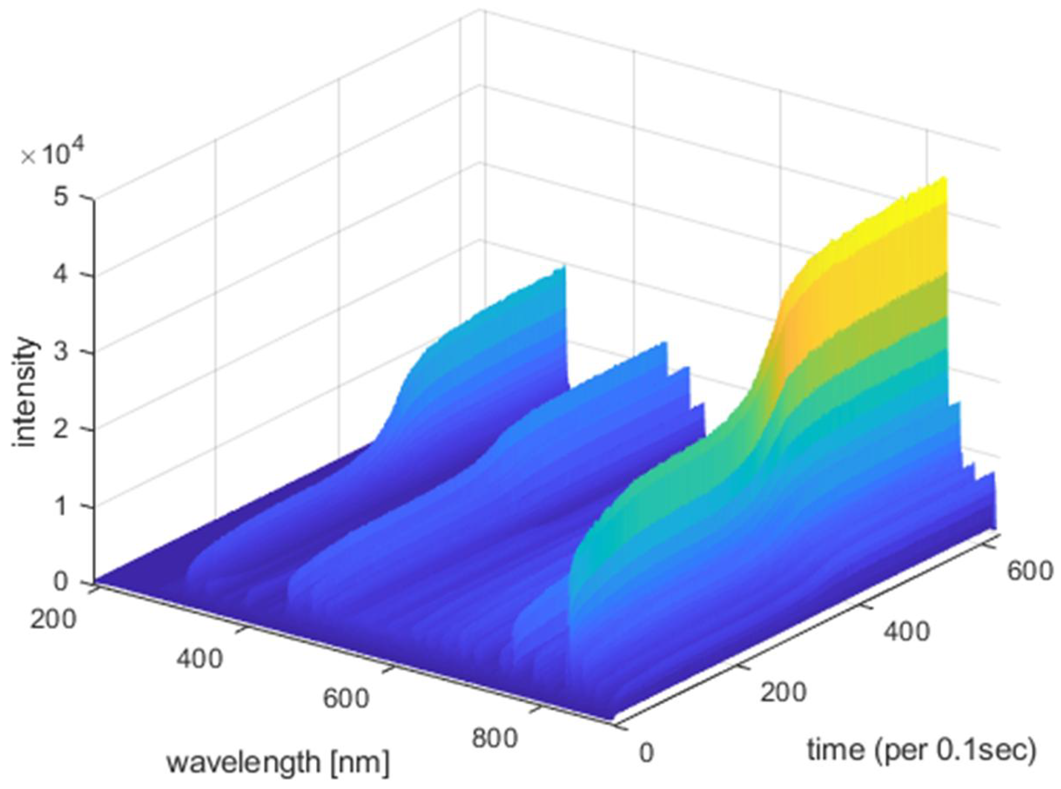
However, the OES data are vast and multi-dimensional as a function of wavelength, time, and intensity, and high-resolution data are required to provide required sensitivity and accuracy for EPD as the feature size decreases. The signal of emission spectra can be weak, and thus the existing simple method of tracking a few selected wavelengths may be insufficient for advanced technology nodes.
Figure 4 shows a sample of actual OES data used in this work. The collected spectra range from 190.0 to 892.8 nm, and the sampling rate is 0.1 sec for about 60 sec.
Figure 5 shows the intensity fluctuations of the wavelengths of 440.1 nm, 516.5 nm, 777.06 nm, which are related to
and
with respect to time. The red line denotes the ground truth EPD time.
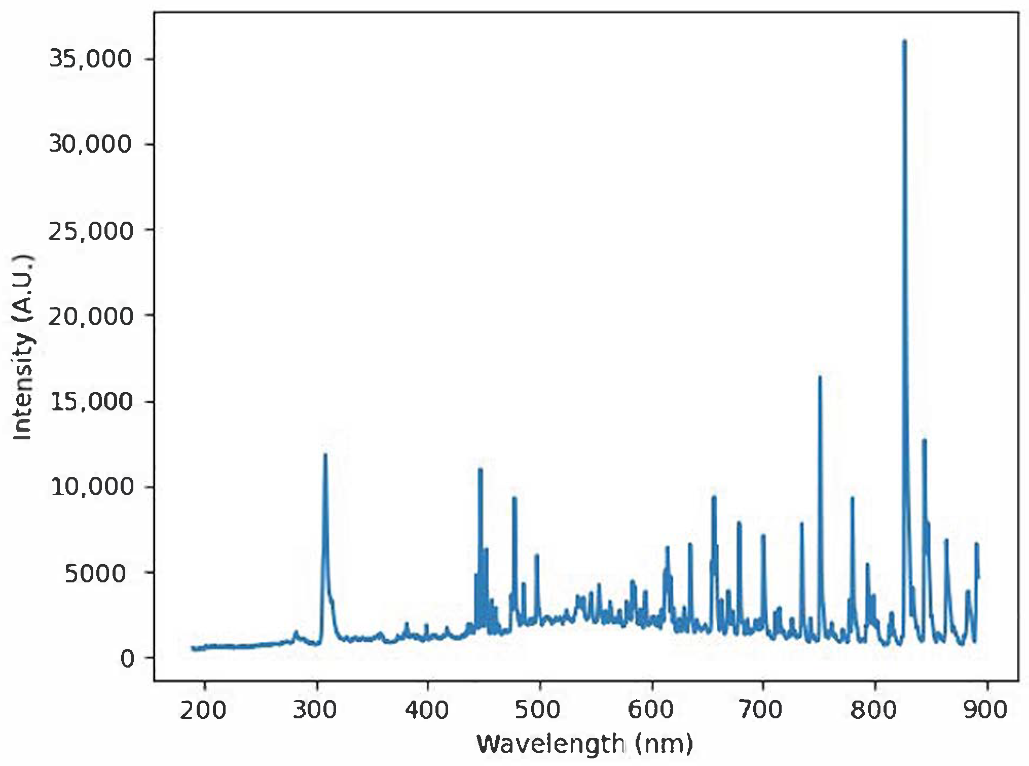
Figure 6 illustrates one sample of the intensity patterns of each wavelength at the EPD time. To handle thousands of such OES data, feature extraction and the aforementioned CNN model are adopted.
3.2. Feature Extraction
Figure 7 illustrates the structure of the training data selection process. In the figure, the vertical axis represents wavelength, while the horizontal axis is sample time. One column denotes the 2048 × 1 vector, whose component represents each wavelength’s intensity.
The training data set consists of endpoint vectors selected in the endpoint block and non-endpoint vectors, randomly selected in the Non-End Point block. Three consecutive vectors are selected in the known endpoint time block and mapped to one for supervised learning. For the non-endpoint data, three vectors are randomly extracted using the random function after excluding the forward ten blocks of the endpoint. The reason for using three vectors is that the accuracy and loss of the model improve compared to extracting one vector and five vectors.
The total OES data are obtained for 2046 wafers, which are processed using two chambers, but in this study, each chamber’s characteristics are not considered. 1911 OES data are randomly chosen for the training data, while the remaining 135 data are allocated for the test data. Using 1911 OES data, 5733 endpoint feature vectors, and 5733 non-end point feature vectors are acquired, as mentioned above. To prevent the overfitting of the model, the ratio of the number of endpoint and non-end point features is equalized. In the experiment, various data ratios, such as 8:2 and 6:4, are tested, but the ratio of 5:5 demonstrates the highest accuracy. After selecting the training data, a random function is applied to separate the training data and the validation data at an 8:2 ratio. As a result, the feature vector set is separated into 9172 training data and 2294 validation data.
4. Experiment and Results
In this section, the performance of the proposed CNN-based model is evaluated using the data described in the previous section and for the purpose of comparison, the SVM and the Adaboost are also employed to detect EPD time using the same feature vector. In the CNN-based model, the 2048 × 1 feature vector is transformed into a matrix form and the other two models use the feature vector as given. The models are developed using Keras with Tensorflow of Python 3.7 in the background, and the computing environment used in the experiments is implemented with an 8-core 3.7-GHz CPU, 32GB of RAM, and an RTX 2080 super GPU.
Three tests are carried out to verify the performance of the three learned models. In the first test, the accuracy is evaluated by using 20% random validation data that are not involved in the learning phase. In the second test, the means and variances of the detection time of the three models are compared using 135 data sets. Each of these data sets contains about 600 consecutive feature vectors of 2048 × 1 according to time. The number of feature vectors in the set is varying depending on its EPD time. The accuracy and variance of the CNN-based model are investigated according to the number of the feature vectors that are selected in the EPD and Non EPD blocks.
4.1. Model Accuracy Test
The model accuracy is evaluated by comparing the model prediction outputs with the ground truth. The third-order SVM classifier demonstrates an accuracy of 99.3%. The Adaboost ensemble classifier achieves an accuracy of 99.17%. CNN shows an accuracy of 99.81%. As a result, the CNN performance was the highest among the three models. These accuracy results are summarized in
Table 2.
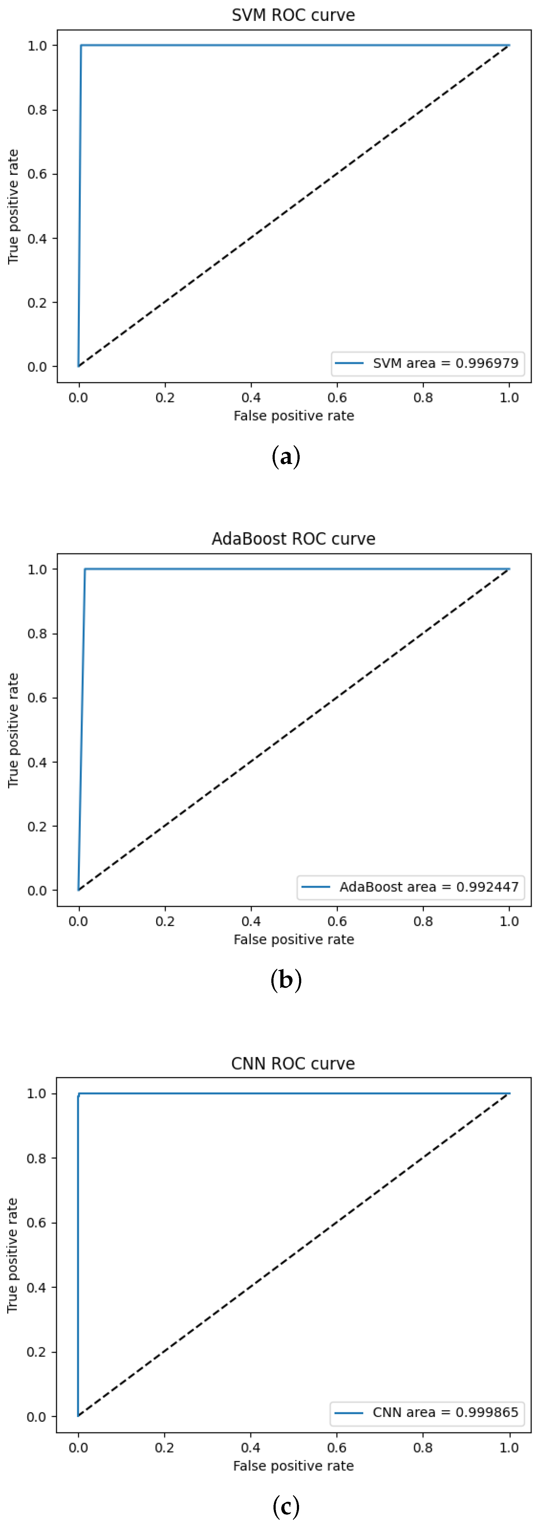
In addition, the receiver operating characteristic (ROC) curve and area under the curve (AUC) of each model are investigated and shown in
Figure 8. As observed in the figure, the AUC of SVM is 0.996979, AdaBoost is 0.992447, and CNN is 0.999865. According to [
47], AUC greater than
indicates that the model achieves outstanding detection performance.
4.2. First Endpoint Detection
This test is performed with the 135 test datasets, which are not involved in the learning. Each dataset contains the feature vectors, as shown in
Figure 4. The size of the vector is 2048 by 1, and its number depends on its EPD time, usually about 600.
In the test, all spectral data over time are applied as inputs to evaluate the endpoint detection performance in the actual etching process. That is, each feature vector of one dataset is sequentially applied to each learned model, and the learned model responds one or zero according to the feature vector, in which one represents EPD and zero does Non-EPD. In this test, the time point when the first EPD (one) appears for the first time is measured for each dataset. The test is carried out for the three models using the 135 datasets.
Figure 9 shows the average of 135 results obtained with the first endpoint detection test. On average, the first endpoint detection of the SVM classifier is 10.79 blocks ahead of the actual endpoint, that of the Adaboost Ensemble classifier is 6.91 blocks ahead, and the CNN is 5.96 blocks ahead. The three models’ commonality in this test is that the endpoint is continuously detected without false detection after the initial detection. Therefore, if the appropriate number of continuous detections is set, the result will match the actual endpoint.
Figure 10 shows the histogram plots of 135 test results for the first endpoint detection test, and
Table 3 summarizes their averages, standard deviations, and variances for the three models. As observed in
Figure 10 and
Table 3, in terms of accuracy and variance, the CNN based model is superior to the other two models. For the two previous experiments, the CNN based model outperforms the third-order SVM classifier and the Adaboost ensemble classifier.
4.3. Overfitting
The previous experiments show that the CNN-based model is relatively better than the remaining two models. In this section, further investigation is carried out for the CNN-based model regarding overfitting and feature size.
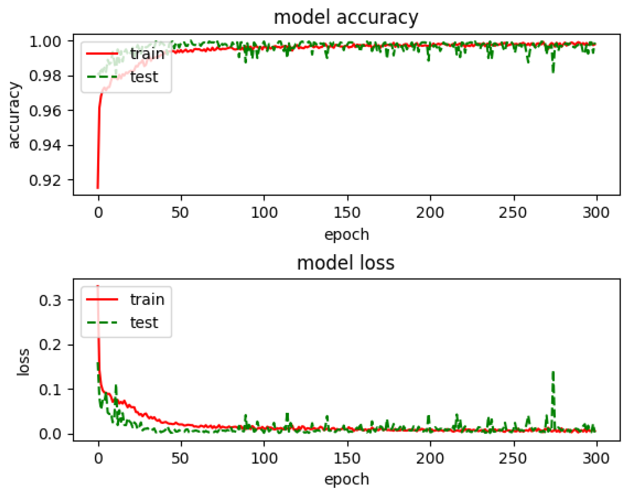
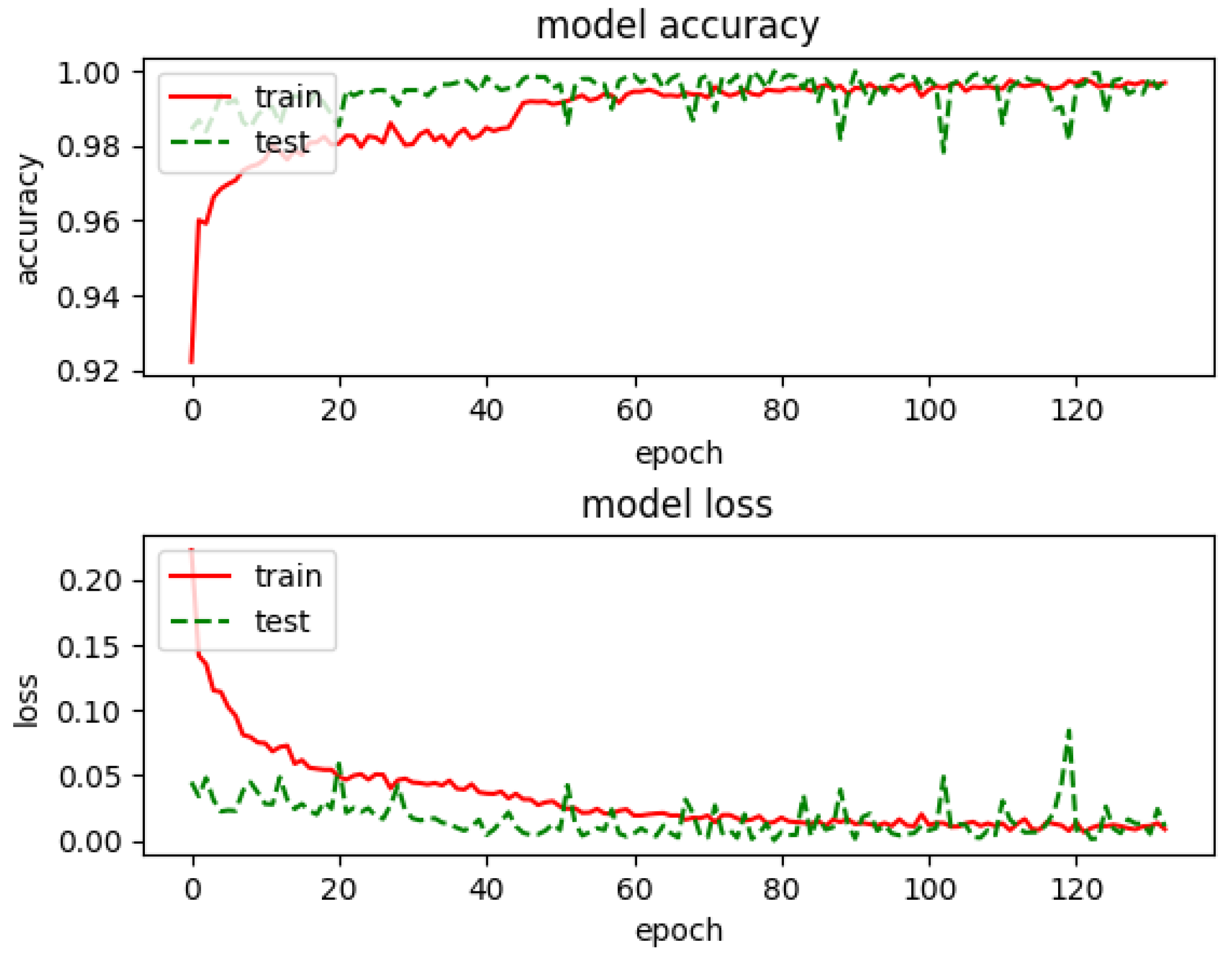
First, to investigate the overfitting of the CNN-based model, the accuracy and loss of the CNN based model are plotted for 300 epochs in
Figure 11. The figure reveals that the validation loss does not decrease any more after around epoch 150 compared to the training loss, which can be regarded as overfitting. To overcome this, the early stopping technique [
48] is employed to train with the appropriate number of epochs. In
Figure 12, the accuracy and loss of the CNN-based model, which is trained with the early stopping technique. In this experiment, the early stopping technique terminates the learning phase at 132 epochs.
5. Conclusions
In this paper, the CNN-based endpoint detection performance was investigated in terms of model accuracy and first endpoint detection time compared to those of the third-order SVM classifier and the Adaboost ensemble classifier. Besides, to prevent overfitting, the application of the early stopping technique is investigated. It is observed that the performance of the CNN-based model is better than the other two classifiers for the two investigations. Considering the results of the CNN-based model obtained in such a non-optimized situation, it is expected that the artificial intelligence technique using the neural network will greatly contribute to the improvement of the accuracy of the endpoint detection technique. In the future, for the model to be applied to the real process environments, an approach based on reinforced learning is required to be further investigated for the model.
Author Contributions
All authors contributed to writing, reviewing, and editing the paper. All authors have read and agreed to the published version of the manuscript.
Funding
This work was supported by Institute of Information & communications Technology Planning & Evaluation (IITP) grant funded by the Korea government (MSIT) (No. 2020-0-02102-001, Development of AI-based 4-channel optical spectrum analysis platform for real-time process diagnostics of semiconductor etching equipment).
Institutional Review Board Statement
Not applicable.
Informed Consent Statement
Not applicable.
Data Availability Statement
Restrictions apply to the availability of these data. Data were obtained from Prime Solution Co., LTD., and are available from the authors with the permission of Prime Solution Co., LTD.
Acknowledgments
The authors would like to express thanks to Prime Solution Co., LTD. for providing the experiment data sets.
Conflicts of Interest
The authors declare no conflict of interest.
References
- Tarca, A.L.; Carey, V.J.; Chen, X.W.; Romero, R.; Drăghici, S. Machine learning and its applications to biology. PLoS Comput. Biol. 2007, 3, e116. [Google Scholar] [CrossRef] [PubMed]
- Yu, L.; Wang, S.; Lai, K.K.; Wen, F. A multiscale neural network learning paradigm for financial crisis forecasting. Neurocomputing 2010, 73, 716–725. [Google Scholar] [CrossRef]
- Nguyen, T.T.; Armitage, G. A survey of techniques for internet traffic classification using machine learning. IEEE Commun. Surv. Tutorials 2008, 10, 56–76. [Google Scholar] [CrossRef]
- Grau, V.; Mewes, A.; Alcaniz, M.; Kikinis, R.; Warfield, S.K. Improved watershed transform for medical image segmentation using prior information. IEEE Trans. Med Imaging 2004, 23, 447–458. [Google Scholar] [CrossRef] [PubMed]
- Ghahramani, Z. Probabilistic machine learning and artificial intelligence. Nature 2015, 521, 452–459. [Google Scholar] [CrossRef] [PubMed]
- Neto, A.H.; Fiorelli, F.A.S. Comparison between detailed model simulation and artificial neural network for forecasting building energy consumption. Energy Build. 2008, 40, 2169–2176. [Google Scholar] [CrossRef]
- Marozzo, F.; Talia, D.; Trunfio, P. A workflow management system for scalable data mining on clouds. IEEE Trans. Serv. Comput. 2016, 11, 480–492. [Google Scholar] [CrossRef]
- Jothi, N.; Rashid, N.A.; Husain, W. Data mining in healthcare—A review. Procedia Comput. Sci. 2015, 72, 306–313. [Google Scholar] [CrossRef]
- Litjens, G.; Kooi, T.; Bejnordi, B.E.; Setio, A.A.A.; Ciompi, F.; Ghafoorian, M.; Van Der Laak, J.A.; Van Ginneken, B.; Sánchez, C.I. A survey on deep learning in medical image analysis. Med. Image Anal. 2017, 42, 60–88. [Google Scholar] [CrossRef]
- Haddad, B.M.; Yang, S.; Karam, L.J.; Ye, J.; Patel, N.S.; Braun, M.W. Multifeature, sparse-based approach for defects detection and classification in semiconductor units. IEEE Trans. Autom. Sci. Eng. 2016, 15, 145–159. [Google Scholar] [CrossRef]
- Susto, G.A.; Beghi, A. Dealing with time-series data in predictive maintenance problems. In Proceedings of the 2016 IEEE 21st International Conference on Emerging Technologies and Factory Automation (ETFA), Berlin, Germany, 6–9 September 2016; pp. 1–4. [Google Scholar]
- Heng, A.; Tan, A.C.; Mathew, J.; Montgomery, N.; Banjevic, D.; Jardine, A.K. Intelligent condition-based prediction of machinery reliability. Mech. Syst. Signal Process. 2009, 23, 1600–1614. [Google Scholar] [CrossRef]
- Köksal, G.; Batmaz, İ.; Testik, M.C. A review of data mining applications for quality improvement in manufacturing industry. Expert Syst. Appl. 2011, 38, 13448–13467. [Google Scholar] [CrossRef]
- Irani, K.B.; Cheng, J.; Fayyad, U.M.; Qian, Z. Applying machine learning to semiconductor manufacturing. IEEE Expert 1993, 8, 41–47. [Google Scholar] [CrossRef]
- Susto, G.A.; Terzi, M.; Beghi, A. Anomaly detection approaches for semiconductor manufacturing. Procedia Manuf. 2017, 11, 2018–2024. [Google Scholar] [CrossRef]
- Braha, D.; Shmilovici, A. Data mining for improving a cleaning process in the semiconductor industry. IEEE Trans. Semicond. Manuf. 2002, 15, 91–101. [Google Scholar] [CrossRef]
- Lin, S.Y.; Horng, S.C. A classification-based fault detection and isolation scheme for the ion implanter. IEEE Trans. Semicond. Manuf. 2006, 19, 411–424. [Google Scholar] [CrossRef]
- Luo, M.; Xu, Z.; Chan, H.L.; Alavi, M. Online predictive maintenance approach for semiconductor equipment. In Proceedings of the IECON 2013-39th Annual Conference of the IEEE Industrial Electronics Society, Vienna, Austria, 10–13 November 2013; pp. 3662–3667. [Google Scholar]
- Mobley, R.K. An Introduction to Predictive Maintenance; Elsevier: Amsterdam, The Netherlands, 2002. [Google Scholar]
- Su, Y.C.; Cheng, F.T.; Hung, M.H.; Huang, H.C. Intelligent prognostics system design and implementation. IEEE Trans. Semicond. Manuf. 2006, 19, 195–207. [Google Scholar] [CrossRef]
- Nakata, K.; Orihara, R.; Mizuoka, Y.; Takagi, K. A comprehensive big-data-based monitoring system for yield enhancement in semiconductor manufacturing. IEEE Trans. Semicond. Manuf. 2017, 30, 339–344. [Google Scholar] [CrossRef]
- Kang, B.S.; Lee, J.H.; Shin, C.K.; Yu, S.J.; Park, S.C. Hybrid machine learning system for integrated yield management in semiconductor manufacturing. Expert Syst. Appl. 1998, 15, 123–132. [Google Scholar] [CrossRef]
- Lenz, B.; Barak, B. Data mining and support vector regression machine learning in semiconductor manufacturing to improve virtual metrology. In Proceedings of the 2013 46th Hawaii International Conference on System Science, Maui, HI, USA, 7–10 January 2013; pp. 3447–3456. [Google Scholar]
- Baly, R.; Hajj, H. Wafer classification using support vector machines. IEEE Trans. Semicond. Manuf. 2012, 25, 373–383. [Google Scholar] [CrossRef]
- Ding, D.; Torres, J.A.; Pan, D.Z. High performance lithography hotspot detection with successively refined pattern identifications and machine learning. IEEE Trans. Comput. Aided Des. Integr. Circuits Syst. 2011, 30, 1621–1634. [Google Scholar] [CrossRef]
- Kim, B.; Kim, D.W.; Park, G.T. Prediction of plasma etching using a polynomial neural network. IEEE Trans. Plasma Sci. 2003, 31, 1330–1336. [Google Scholar]
- Jimenez-Fernandez, V.M.; Reyes-Betanzo, C.; Angelica-Cerdan, M.; Hernandez-Paxtian, Z.J.; Vazquez-Leal, H.; Itzmoyotl-Toxqui, A. Prediction of silicon dry etching using a piecewise linear algorithm. J. Chin. Inst. Eng. 2013, 36, 941–950. [Google Scholar] [CrossRef]
- Kim, B.; Lee, D.W.; Kwon, K.H. Prediction of etch microtrenching using a neural network. J. Appl. Phys. 2004, 96, 3612–3616. [Google Scholar] [CrossRef]
- Kim, B.; Bae, J.; Lee, B.T. Modeling of silicon oxynitride etch microtrenching using genetic algorithm and neural network. Microelectron. Eng. 2006, 83, 513–519. [Google Scholar] [CrossRef]
- Kanoh, M.; Yamage, M.; Takada, H. End-point detection of reactive ion etching by plasma impedance monitoring. Jpn. J. Appl. Phys. 2001, 40, 1457. [Google Scholar] [CrossRef]
- Chen, R.; Huang, H.; Spanos, C.; Gatto, M. Plasma etch modeling using optical emission spectroscopy. J. Vac. Sci. Technol. Vacuum Surf. Film. 1996, 14, 1901–1906. [Google Scholar] [CrossRef]
- Yue, H.H.; Qin, S.J.; Wiseman, J.; Toprac, A. Plasma etching endpoint detection using multiple wavelengths for small open-area wafers. J. Vac. Sci. Technol. Vacuum Surf. Film. 2001, 19, 66–75. [Google Scholar] [CrossRef]
- Jang, H.; Lee, H.; Lee, H.; Kim, C.K.; Chae, H. Sensitivity Enhancement of Dielectric Plasma Etching Endpoint Detection by Optical Emission Spectra With Modified K-Means Cluster Analysis. IEEE Trans. Semicond. Manuf. 2017, 30, 17–22. [Google Scholar] [CrossRef]
- Noh, H.T.; Kim, D.I.; Han, S.S. Real time endpoint detection in plasma etching using Real-Time Decision Making Algorithm. In Proceedings of the 2015 China Semiconductor Technology International Conference, Shanghai, China, 15–16 March 2015; pp. 1–3. [Google Scholar]
- Han, K.; Yoon, E.S.; Lee, J.; Chae, H.; Han, K.H.; Park, K.J. Real-time end-point detection using modified principal component analysis for small open area SiO2 plasma etching. Ind. Eng. Chem. Res. 2008, 47, 3907–3911. [Google Scholar] [CrossRef]
- Hong, S.J.; May, G.S.; Park, D.C. Neural network modeling of reactive ion etching using optical emission spectroscopy data. IEEE Trans. Semicond. Manuf. 2003, 16, 598–608. [Google Scholar] [CrossRef]
- Kenney, J.; Valcore, J.; Riggs, S.; Rietman, E. Deep Learning Regression of VLSI Plasma Etch Metrology. arXiv 2019, arXiv:1910.10067. [Google Scholar]
- Azamfar, M.; Li, X.; Lee, J. Deep Learning-Based Domain Adaptation Method for Fault Diagnosis in Semiconductor Manufacturing. IEEE Trans. Semicond. Manuf. 2020, 33, 445–453. [Google Scholar] [CrossRef]
- Maggipinto, M.; Beghi, A.; McLoone, S.; Susto, G.A. DeepVM: A Deep Learning-based Approach with Automatic Feature Extraction for 2D Input Data Virtual Metrology. J. Process Control 2019, 84, 24–34. [Google Scholar] [CrossRef]
- Gu, J.M.; Thadesar, P.A.; Dembla, A.; Bakir, M.S.; May, G.S.; Hong, S.J. Endpoint detection in low open area TSV fabrication using optical emission spectroscopy. IEEE Trans. Components Packag. Manuf. Technol. 2014, 4, 1251–1260. [Google Scholar]
- Santos, P.; Villa Montoya, L.; Reñones, A.; Bustillo, A.; Maudes, J. An SVM-Based Solution for Fault Detection in Wind Turbines. Sensors 2015, 15, 5627–5648. [Google Scholar] [CrossRef]
- Jain, U.; Nathani, K.; Ruban, N.; Raj, A.N.J.; Zhuang, Z.; Mahesh, V.G. Cubic SVM Classifier Based Feature Extraction and Emotion Detection from Speech Signals. In Proceedings of the 2018 International Conference on Sensor Networks and Signal Processing (SNSP), Xi’an, China, 28–31 October 2018; pp. 386–391. [Google Scholar]
- Kwon, O.W.; Lee, T.W. Optimizing speech/non-speech classifier design using AdaBoost. In Proceedings of the 2003 IEEE International Conference on Acoustics, Speech, and Signal Processing (ICASSP ’03). Hong Kong, China, 6–10 April 2003; Volume 1, pp. I-436–I-439. [Google Scholar] [CrossRef]
- Viola, P.; Jones, M.J. Robust real-time face detection. Int. J. Comput. Vis. 2004, 57, 137–154. [Google Scholar] [CrossRef]
- Shaheen, F.; Verma, B.; Asafuddoula, M. Impact of automatic feature extraction in deep learning architecture. In Proceedings of the 2016 International Conference on Digital Image Computing: Techniques and Applications (DICTA), Gold Coast, Australia, 30 November–2 December 2016; pp. 1–8. [Google Scholar]
- Litvak, H.E. End point control via optical emission spectroscopy. J. Vac. Sci. Technol. Microelectron. Nanometer Struct. Process. Meas. Phenom. 1996, 14, 516–520. [Google Scholar] [CrossRef]
- Hosmer, D.W., Jr.; Lemeshow, S.; Sturdivant, R.X. Applied Logistic Regression; John Wiley & Sons: Hoboken, NJ, USA, 2013; Volume 398. [Google Scholar]
- Caruana, R.; Lawrence, S.; Giles, C.L. Overfitting in neural nets: Backpropagation, conjugate gradient, and early stopping. In Advances in Neural Information Processing Systems; MIT Press: Cambridge, MA, USA, 2001; pp. 402–408. [Google Scholar]
| Publisher’s Note: MDPI stays neutral with regard to jurisdictional claims in published maps and institutional affiliations. |
© 2020 by the authors. Licensee MDPI, Basel, Switzerland. This article is an open access article distributed under the terms and conditions of the Creative Commons Attribution (CC BY) license (http://creativecommons.org/licenses/by/4.0/).


