Article

Influence of Growth Polarity Switching on the Optical and Electrical Properties of GaN/AlGaN Nanowire LEDs

1
Institute of Physics, Polish Academy of Sciences, Aleja Lotnikow 32/46, PL-02668 Warsaw, Poland
2
Faculty of Physics, University of Warsaw, Pasteura 5, PL-02093 Warsaw, Poland
3
Institute of Photonics and Electronics, Czech Academy of Sciences, Chaberská 57, 18251 Praha 8-Kobylisy, Czech Republic
4
Institute of High Pressure Physics, Polish Academy of Sciences, Sokołowska 29/37, PL-01142 Warsaw, Poland
5
Paul-Drude-Institut für Festkörperelektronik, Hausvogteiplatz 5–7, D-10117 Berlin, Germany
*
Author to whom correspondence should be addressed.
Electronics 2021, 10(1), 45; https://doi.org/10.3390/electronics10010045
Submission received: 12 October 2020 / Revised: 21 December 2020 / Accepted: 23 December 2020 / Published: 29 December 2020
(This article belongs to the Special Issue Micro- and Nanotechnology of Wide Bandgap Semiconductors)

Abstract

:
For the development and application of GaN-based nanowire structures, it is crucial to understand their fundamental properties. In this work, we provide the nano-scale correlation of the morphological, electrical, and optical properties of GaN/AlGaN nanowire light emitting diodes (LEDs), observed using a combination of spatially and spectrally resolved cathodoluminescence spectroscopy and imaging, electron beam-induced current microscopy, the nano-probe technique, and scanning electron microscopy. To complement the results, the photo- and electro-luminescence were also studied. The interpretation of the experimental data was supported by the results of numerical simulations of the electronic band structure. We characterized two types of nanowire LEDs grown in one process, which exhibit top facets of different shapes and, as we proved, have opposite growth polarities. We show that switching the polarity of nanowires (NWs) from the N- to Ga-face has a significant impact on their optical and electrical properties. In particular, cathodoluminescence studies revealed quantum wells emissions at about 3.5 eV, which were much brighter in Ga-polar NWs than in N-polar NWs. Moreover, the electron beam-induced current mapping proved that the p–n junctions were not active in N-polar NWs. Our results clearly indicate that intentional polarity inversion between the n- and p-type parts of NWs is a potential path towards the development of efficient nanoLED NW structures.

1. Introduction

While light emitting diodes (LEDs) or laser diodes (LDs) made of group III nitrides have widely replaced conventional light sources in everyday life and various brands of technology [1,2,3], they still suffer from drawbacks such as a limited internal quantum efficiency and low light extraction efficiency. These problems are related to structural imperfections (such as a high dislocation density), strong polarization electric fields at interfaces, or inefficient doping in the planar multilayer structures, which are composed of materials with markedly different structural parameters. One solution to at least some of those problems that has been seriously considered is to replace continuous layers of semiconductors with ensembles of quasi-1D nanowires (NWs) grown perpendicularly to the substrate.
III-N compounds and their solid solutions are highly suitable for the construction of photonic devices. Their band gap energies cover a wide range from 0.7 eV for InN, through 3.4 eV for GaN, to 6.1 eV for AlN [4]. In principle, appropriate selection of the nitride composition in the active region of an optoelectronic device should allow for the obtention of electromagnetic radiation from any part of the visible spectrum or a considerable part of the ultraviolet band. Thus, they can be used in the fabrication of lighting systems imitating the daylight spectrum for houses and offices; light source-acceleration of photosynthesis for agriculture; and health care applications. Additionally, full-color displays or high-density optical data storage systems based on nitride laser diodes can be produced. Nitride-based optoelectronic devices can also be applied in UV detection [5,6] for aerospace and automotive engineering, biology/medicine, and astronomy. All the components of these devices, such as quantum wells, barriers, and p- and n-type layers in heterojunctions, can be fabricated from proper nitrides or their alloys. This is an important advantage of group III nitrides compared to many other wide-band-gap materials. Nevertheless, technical problems associated with the complex synthesis of multilayer semiconductor structures make the reproducible fabrication of reliable devices challenging. It is of great importance to select substrates that are lattice-matched and thermally compatible, while also large and cost-effective. While ammonothermal [7,8] and hydride vapor-phase epitaxy (HVPE) [9,10] methods of growing large bulk GaN substrates have already been successfully developed, sapphire or SiC substrates are still routinely used and have shown promising results. The growth of high-quality nitride structures on silicon would make the integration of nitride-based devices with advanced Si microelectronics possible. This would provide a great advancement in optoelectronic device technology.
The lattice mismatch between the substrate and the nitride layer results in dislocations, relieving the strain at the interface but deteriorating the electrical and optical properties of the structure. Various methods, such as buffer layer engineering and the epitaxial lateral overgrowth technique, have been devised to reduce the dislocation density in nitride-layered structures. Replacing 2D layers with a set of quasi 1D NWs improves the strain accommodation conditions at the markedly smaller interface. This effect was also demonstrated for nitride NWs grown on a Si substrate [11]. The appearance of stress-relieving dislocations can be avoided not only between the substrate and the nanowire but also at the interfaces inside the nanowire [12].
The quasi 1D geometry of the structure has more advantages than those already mentioned: For nano-light-emitters created as axial or radial heterostructures, it increases the light generation efficiency; reduces the light losses in the structure; enhances the efficacy of light extraction from the structure; and allows for the growth of multicolor micro-LED pixels [13,14,15]. Such objects, with a regular shape defined by the crystalline structure and a size comparable to the wavelength of light, can also confine electro-magnetic radiation and play the role of a resonator for such nano-devices. However, some other critical issues influencing the functionality of nanowire-based devices still exist. It is necessary to solve the problems associated with effective p-type doping (in particular, for ternaries with high In or Al contents) in order to reduce defect-related nonradiative recombination channels, including those related to the developed surface of the system. This would improve hole transport, which is limited by defects, and thus tackle the heat management issue in quasi 1D devices. Some of these issues, such as p-type doping, defect creation (e.g., defects caused by stacking faults (SFs) and polarity inversion domains) are directly related to the nanowire growth conditions.
An important feature of NWs is the possibility of fabricating them by a bottom-up growth process, without the use of technically demanding and expensive technological processes, such as photo- or electron-beam lithography, resist deposition, or etching. Instead, the spontaneous formation of NWs governed by the growth conditions is often applied. A variety of growth methods allowing for the fabrication of NWs on various substrates have been successfully tested (including chemical vapor deposition, metalorganic chemical vapor deposition (MOCVD), and molecular beam epitaxy (MBE) [16]), and numerous examples of ensembles of NWs that are of a highly crystalline quality and have well defined electronic and optical properties have been demonstrated (for a review, see [17]).
Among the techniques currently used to grow III-N low-dimensional structures, MBE has important advantages. The high purity of the source materials and ultra-high-vacuum growth conditions, as well as the availability of many techniques of in-situ growth monitoring, allow for a reduction in the unintentional impurity level and improvement in the crystalline quality of the grown material. In general, the two most commonly used approaches to nanowire growth by MBE are based on spontaneous nucleation and vapor-liquid-solid growth, in which whiskers are grown beneath a catalyst droplet. The former [18] is routinely used to grow nitride NWs, since it eliminates the unwanted contamination of NWs with catalyst atoms. While the MBE method is not suitable for the mass production of devices, it is a convenient tool for studies motivated mainly by an interest in fundamental physical processes involving electrons and photons in NWs. The structure of NWs can be carefully controlled and modified in accordance with the results of microscopic, structural, and optical measurements, even if some uncertainties concerning the NW size or composition, resulting from the spontaneous nature of the growth process, should be borne in mind. However, the conclusions can lead to improvements in the architecture and technology of real devices or, at least, the construction of demonstrator devices.
Full control of the course of the growth process and properties of the resulting system is still far from being established. This leads to a scattering of the important physical properties of NWs, even those obtained on the same substrate in a single process. The inner structure of the nanorods may contain spontaneously formed defects, chemical composition fluctuations, domains with built-in strain, growth polarity domains, etc. Fingerprints of some of these defects can be detected by cathodo- and photoluminescence, for example, stacking faults [19,20] and inverted polarity domains [21,22]. On the other hand, intentionally grown axial or radial heterojunctions, quantum wells, etc., are formed in the NWs in order to study basic physical phenomena (e.g., those related to elementary excitations in semiconductors) or create new functionalities [13,23]. Since the properties fluctuate between nanowires, the parameters should not be analyzed as global quantities describing the sets of many nanowires. It is necessary to investigate the optical and electronic properties of NWs with a submicron or nanometer resolution, which allows the properties of the sub-structures of NWs, such as quantum wells, barriers, and p- or n-type segments in the heterojunctions to be revealed.
In this work, we report on the nano-scale correlation of the morphological, structural, electrical, and optical properties of GaN/AlGaN nanowire LEDs, as observed by a combination of scanning electron microscopy (SEM), spatially and spectrally resolved cathodoluminescence (CL), andelectron beam-induced current (EBIC), atomic force, and Kelvin probe force microscopies. GaN/AlGaN LED nanowire structures with three GaN quantum wells in the p–n junction and AlGaN barriers were grown on silicon (111) substrates, without any catalyst, using plasma-assisted molecular-beam epitaxy. The bottom n-type part of the structure was made of GaN:Si. Then, the GaN wells sandwiched between AlGaN barriers were formed. The top part of the nanowire, which acted as the p-type part of the p–n junction, was composed of AlGaN:Mg. As this part was employed with the intention of forming a quasi-planar base for the top electrical contact of the structure, the growth mode had to be adapted to the conditions, which enhanced the lateral growth, leading to an inversely tapered form of the NWs. Therefore, the upper part of the structure was formed under particularly demanding conditions, and its properties resulted from the interplay of several coinciding physical phenomena. It was grown from an AlGaN solid solution at a reduced growth temperature and under intense Mg-doping, which should give the p-type conductivity. The results of our investigations indicated that unintentional fluctuations in the growth conditions caused the growth polarity to switch from the N- to the Ga-face for a considerable part of the NWs. Such a polarity reversal causes differences in the growth and changes the direction of the built-in spontaneous electric field [24]. The EBIC signal and the CL spectral features recorded for individual NWs proved that in the N-face NWs, the p–n junctions were not active, and the quantum-well luminescence was reduced. A comparison of the experimental data with the results of the numerical simulations of the electronic band structure of individual NWs facilitated a discussion of the physical mechanisms responsible for the activation or deactivation of the p–n junctions. We ascribed the reduced functionality of the p–n junction to an ineffective Mg-doping of the top part of the NWs grown with N-polarity. This conclusion established the growth parameters that result in the successful growth of functional nanoLEDs in NWs.

2. Samples and Experimental Methods
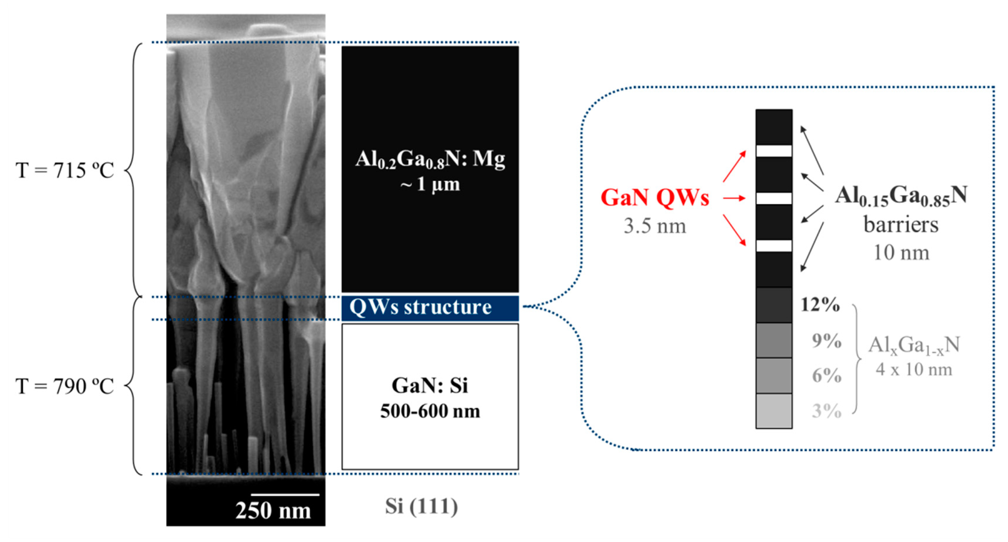
2.1. Samples

The GaN/AlGaN NW LEDs were grown on in-situ nitridated 3” Si (111) substrates using plasma-assisted molecular beam epitaxy (PAMBE) in a Riber Compact 21 system with elemental sources of Ga, Al, Si, and Mg. A radio frequency Addon nitrogen plasma cell, controlled by an optical sensor of plasma light emission [25], was used as the source of active nitrogen species. No catalyst was used to induce the nucleation of the NWs. The nanowire LEDs with the three GaN quantum wells in the area of the p–n junction were grown according to the following procedure. First, the 500–600 nm-long GaN nanowires doped with Si (nominal doping level: 5 × 1018 cm−3) were grown under N-rich conditions at a temperature of 790 °C to achieve the n-type part of the structure. Then, the quantum structure was grown. It began with AlxGa1−xN segments with a gradually increased composition (3%, 6%, 9%, 12%) and was followed by the growth of 3 GaN quantum wells (QWs) with thicknesses of 3.5 nm, which were sandwiched between the 10 nm-thick Al0.15Ga0.85N barriers. The number of QWs and other parameters of the quantum structure were chosen on the basis of our previous experience, and reports are available in the literature (e.g., [26]). As such a configuration provides efficient luminescence, it was suitable for testing the functionality of our nanoLED in NWs. Finally, the p-type part of the structure consisting of 1 µm-thick Al0.2Ga0.8N doped with Mg (nominal doping level: 5 × 1019 cm−3) was grown. The growth temperature at this step was reduced to 715 °C to enhance the lateral growth rate and to broaden the nanowire tops, with the aim of making the further processing of the device easier.
A detailed scheme of the NW LED structure is shown in Figure 1. More details on the growth method used for the fabrication of the NW structures can be found in [27,28,29]. The contact with the n-type (cathode) was obtained by covering the Si substrate with indium (for electroluminescence measurements) or aluminum (for EBIC studies). The anodes were made by the evaporation of a thin, semitransparent layer of gold on the upper surfaces of the NWs. The anodes for the electroluminescence measurements had a shape characterized by circular spots with a diameter of 1 mm. The layer of gold was continuous and conductive due to the good coalescence of the tops of the NWs, which was obtained by their lateral growth.

2.2. Methods

The morphology of the LED NWs was examined by scanning electron microscopy (SEM) using a field-emission Hitachi SU-70 scanning electron microscope (Hitachi, Tokyo, Japan). The SEM machine, equipped with a Gatan MonoCL3 cathodoluminescence system, including the continuous-flow liquid helium cryo-stage and Gatan electron beam induced current (EBIC) setup, enabled studies of the local optical and electrical properties of single NWs.
High-resolution transmission electron microscopy (TEM) experiments of the LED NW structures were conducted using the FEI Titan 80–300 Cubed high-resolution TEM (HRTEM) operating at 300 keV (FEI Company, Hillsboro, ON, USA).
The photoluminescence (PL) spectra were excited by a system composed of a Ti:Sapphire laser and third harmonic generator at a wavelength of 300 nm, with a pulse frequency of 80 MHz. The time-resolved photoluminescence (TRPL) kinetics were measured using a Hamamatsu C5680 streak-camera (Hamamatsu Photonics, Shizuoka, Japan).
The I–V characteristics of individual LED NWs were measured in the chamber of the Tescan Lyra3 scanning electron microscope (Tescan Orsay Holding, a.s., Brno-Kohoutovice, Czech Republic) using a Keithley 236 measurement unit. A tungsten tip of a SmarAct nano-probe served as a top ohmic contact (SmarAct GmbH, Oldenburg, Germany).
The atomic force microscopy (AFM) and Kelvin probe force microscopy (KPFM) were carried out in the tapping mode using a MultiMode AFM, with a Nanoscope IIIa controller and Nanoscope Extender (Bruker/Digital Instruments, Billerica, MA, USA).

3. Results

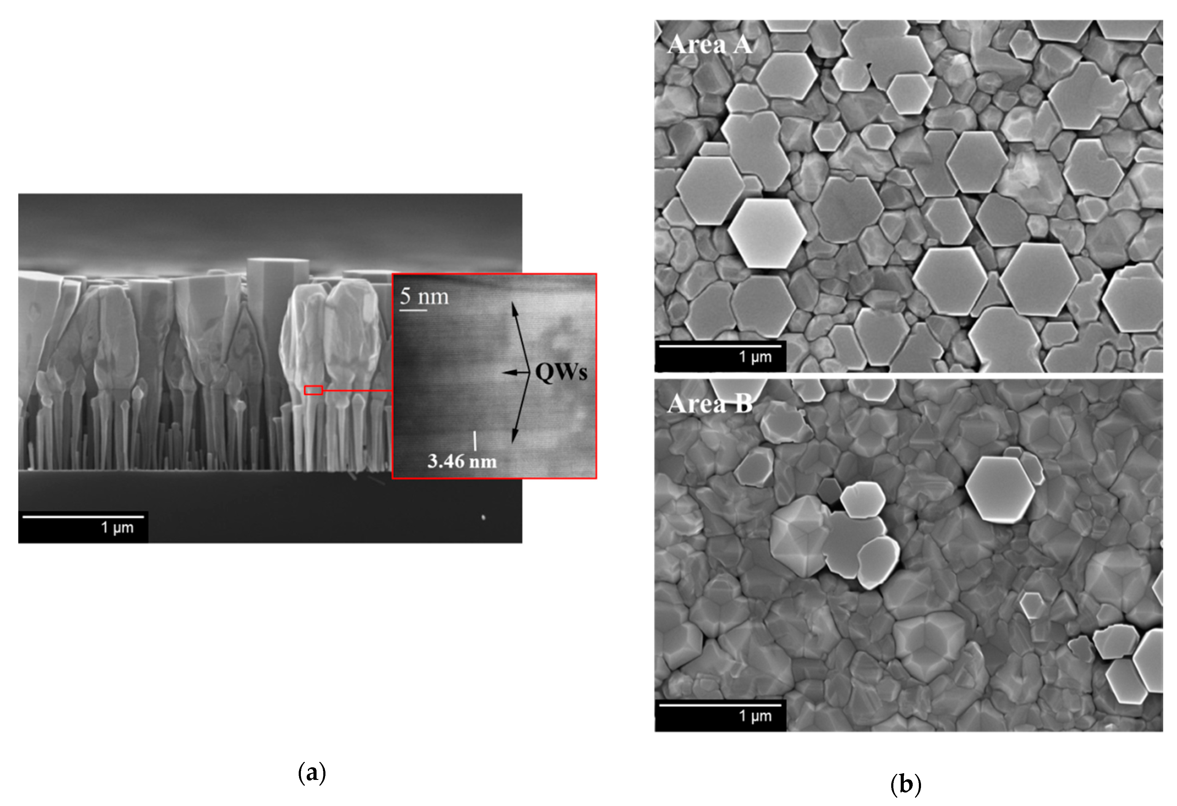
3.1. Morphology and Structure

Despite the fact that the NWs were grown in the same growth process, the SEM investigations revealed two kinds of NW morphologies, as shown in Figure 2.
Figure 2a shows a cross-sectional SEM image, where two types of nanowires can be easily distinguished. Some of them have a regular broadening, with flat sides, and some have an irregular “oval-like” shape in the laterally grown area. In the plane-view SEM (Figure 2b), differences are also clearly visible: some of the NWs have a flat hexagonal top with sharp edges, while the others have a less regular, rough top with rounded edges.
We note that, due to a radial temperature gradient across the wafer, two areas could be easily distinguished on the substrate surface. Area A (Figure 2b, upper panel) is a ~10 mm-wide ring near the edge of the wafer, while area B (Figure 2b, bottom panel) is a circle in the center of the wafer. Independent measurements of the temperature distribution, performed by growing planar GaN layers on such substrates, indicated a ~30 °C higher growth temperature at the wafer periphery than in the central B area. Interestingly, such a temperature profile led to the noticeably higher concentration of hexagonally shaped NWs in area A than in the colder part (area B) of the wafer, as shown in the SEM images.
The TEM studies in the Z-contrast scanning transmission mode (STEM) revealed that both types of NWs contain three 3.5 nm-thick QWs (inset in Figure 2a). The bottom parts and QW regions of NWs are similar in all wires, and differences are observed only in the upper p-type Al0.2Ga0.8N:Mg part of the LED structure. The NWs with the flat hexagonal tops are more uniform, while in the NWs with the “oval-like” top area, some features resembling grain boundaries are visible.
In the [0001] direction, GaN can grow either in the Ga or N direction, which are referred to as polarities. Most nitride layers are grown in the Ga polarity, while spontaneously nucleated GaN NWs usually grow in the N polarity. However, depending on the interface chemistry and the growth procedure, changes to the Ga polarity inside one NW ensemble are often observed. Since the specific polarity of NWs affects both the optical and electrical properties and result in different properties for two morphologically distinct types of NWs, it is necessary to assess the polarity of individual NWs. This was conducted by the selective etching of the sample in an aqueous solution of potassium hydroxide (KOH). The principle of this method is based on the fact that the etching behavior strongly depends on the chemical nature of the surface. The resulting etching rate, etched surface shape, and roughness are determined by the polarity, which can, therefore, be clearly identified. It was revealed in research by several groups that the KOH etching rate is much lower for Ga-polar GaN surfaces than for N-polar ones (see, for instance, [30,31,32,33]).
In our case, the samples were etched in a KOH:H2O 6.5 g/100 mL solution at a temperature of 160 °C for 10 min. SEM images of the samples’ surfaces are presented in Figure 3. In the SEM image of the as-grown sample (Figure 3a), two kinds of NWs are visible—hexagonal- and oval-shaped, as mentioned earlier. Figure 3b presents exactly the same area of the sample, after etching in the KOH solution. It can be seen that the NWs of a hexagonal shape with flat tops have disappeared, while some of the oval-top NWs remain untouched. This experiment proved that the hexagonal-top surfaces were N-polar NWs, while the oval-top ones had Ga polarity.

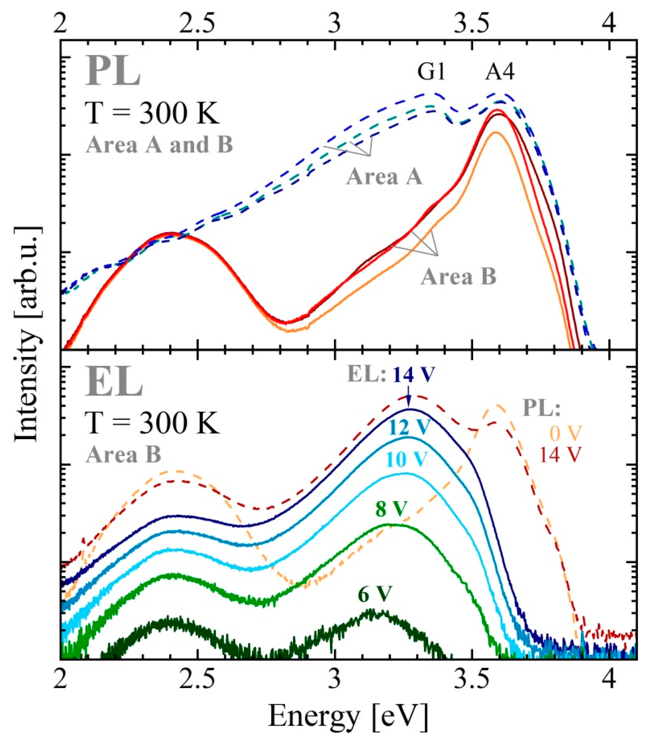
3.2. Macroscopic Electro- and Photoluminescence

The semiconductor structure inside the NW was designed to work as a light emitting diode. The bottom part was n-type (Si-doped), the upper part was p-type (Mg-doped), and three QWs were placed in the region of the p–n junction in order to trap electrons and holes, which should promote radiative recombination. Figure 4 (upper panel) shows the photoluminescence spectra at different points in the sample. It can be observed that the spectra are significantly different. For example, the GaN-related G1 peak is much stronger in the A area, while area B is dominated by AlGaN emission (peak A4). To check the operation of the NW LED devices, a series of small diodes were prepared for macroscopic electroluminescence (EL) measurements in a few rows, from the edge to the center of the wafer, across the A and B areas. After application of a voltage, blue-violet-UV electroluminescence was only observed in the B area. Diodes in the A area, mostly consisting of the hexagonally shaped top facets, were not active, which agrees well with the I–V data shown in Figure 9. The electroluminescence (EL) spectra of the forward polarized ensemble of the NWs in the B area, as a function of the applied voltage, are plotted in Figure 4 (bottom panel).
We note that in order to obtain a sufficient current, it was necessary to apply a bias of the order of 10 V, which was due to the high resistivity of the NWs. The main decrease in the voltage was most probably in the p-type part of the NWs. Nevertheless, the change in bias caused a change in electric field in the area of QWs, which led to a shift in the emission energy from 3.15 eV up to 3.28 eV, with an increase in the bias (see Figure 4—bottom panel). The effect can be explained as state filling due to a high-density electron current or a reduction in the quantum-confined Stark effect (QCSE). In the second case, an increase in the external voltage led to a reduction in the total electric field, which means that the build-in electric field has the opposite direction to that of the external one. Figure 4 shows the photoluminescence (PL) spectra obtained by the photoexcitation of the diode without voltage and PL (plus EL), observed under a bias of 14 V. In the case of EL, electrons are provided by a cathode, while holes are injected by an anode. The only part of the structure that contains both types of carriers is an active region with the QWs. Thus, in EL, only one peak was visible. During light excitations, electrons and holes were generated throughout the structure, so we could also observe the peak A4 at 3.6 eV, which is related to AlGaN. The A4 peak decreased after the application of the voltage, which was probably caused by the increase in the electric field in the AlGaN part. This meant that the build-in electric field existing in AlGaN without application of an external voltage had the same direction as the external field applied in the forward direction. The EL was only observed at room temperature, since at lower temperatures, the sample was not electrically conductive. However, it was possible to measure PL at lower temperatures.
A comparison of PL at 4 and 300 K in the A and B areas can be found in Figure 5. The spectra were measured in the time-resolved mode, and the kinetics of the light emission could be determined. At room temperature (upper panels in Figure 5a,b), the AlGaN-related emission was observed in a range above 3.5 eV. It was diminished by fast relaxation (lifetime about 0.1 ns) due to the escape of carriers to GaN. The main GaN peak, G1, was at about 3.4 eV at 300 K. Its lifetime depended on the location in the sample at which it was measured, from 1 ns in area A to 0.2 ns in the B area. It was observed that the GaN peak at t = 0 was at about 3.4 eV, and its energy decreased to 3.3 eV after 2 ns. Such an effect can be caused by the QCSE in the QWs. Since the energy of this peak coincided with the electroluminescence energy, we can assume that it was emitted by the QWs. Due to a shift in the energy gap [34], the luminescence spectra at 4 K are expected to be at an energy that is about 0.1 eV higher, compared to that at room temperature. The AlGaN emission was observed in the 3.6–3.8 eV range, and the GaN emission was at 3.47 eV (G1) and about 3.43 eV (G2). As can be seen in in the bottom panels of Figure 5a,b, the emission dynamics in the A and B areas were similar. The G1 peak was observed only under a high-power excitation. The lifetimes ranged from 0.2 to 0.5 ns for the AlGaN emission and 1–2 ns for the G2 emission. The exciton lifetimes in 3D GaN were below 1 ns [35], but similarly long lifetimes were observed for QWs [26,36] and SF (which was also compared to QW [20]). Therefore, we assumed that G2 is related to QWs.

3.3. Microscopic Optical and Electrical Properties

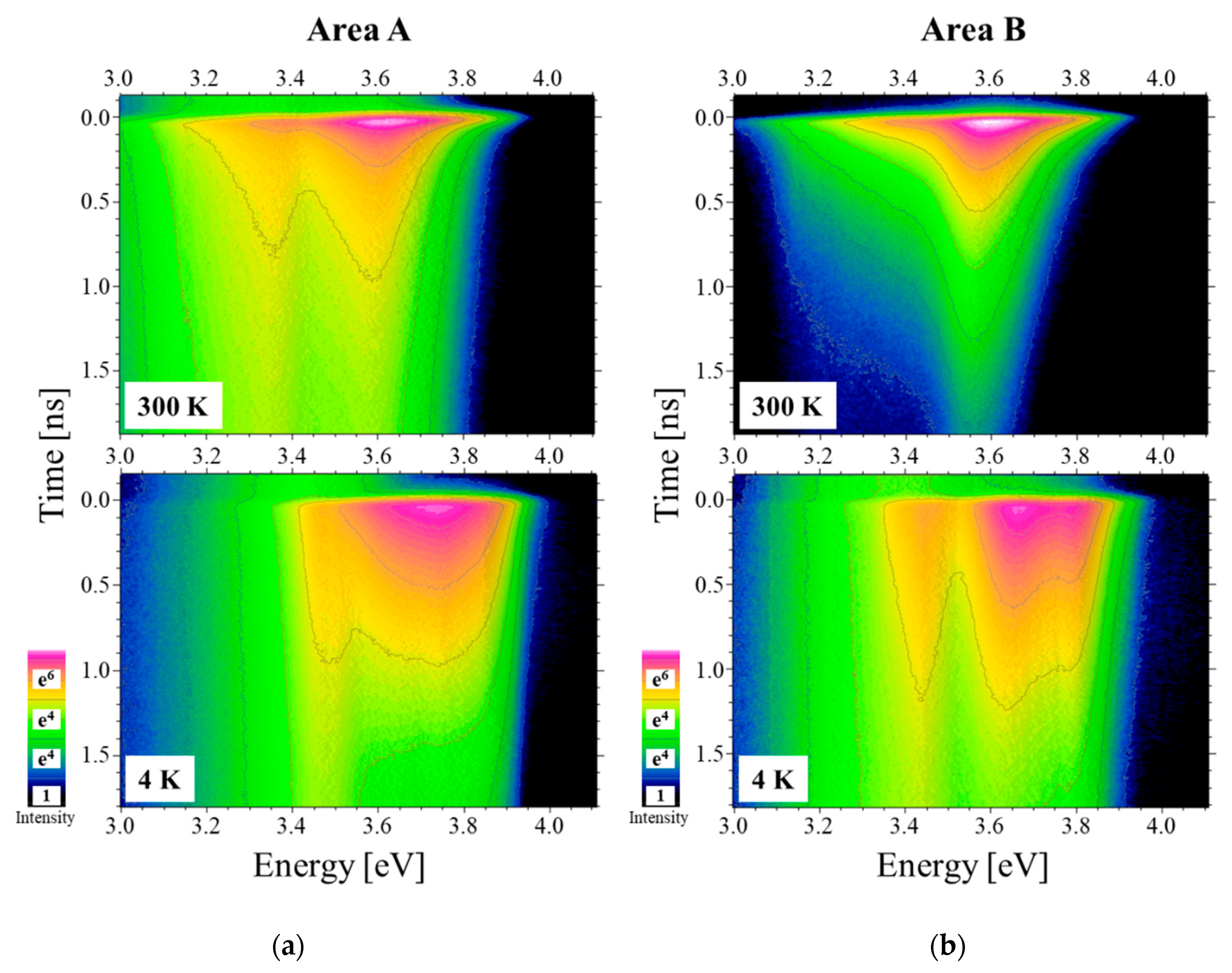
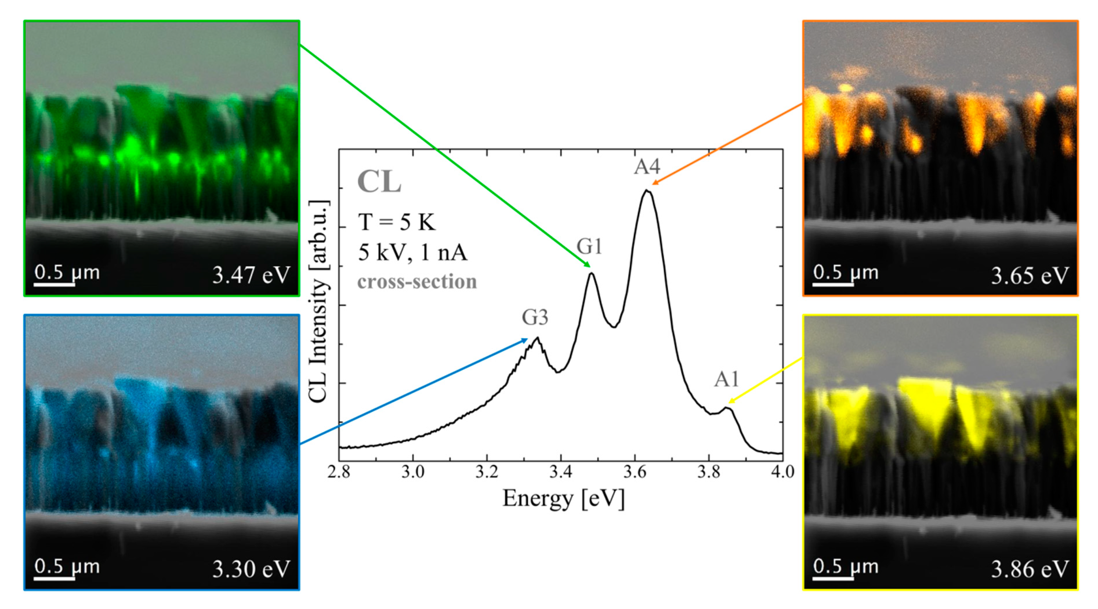
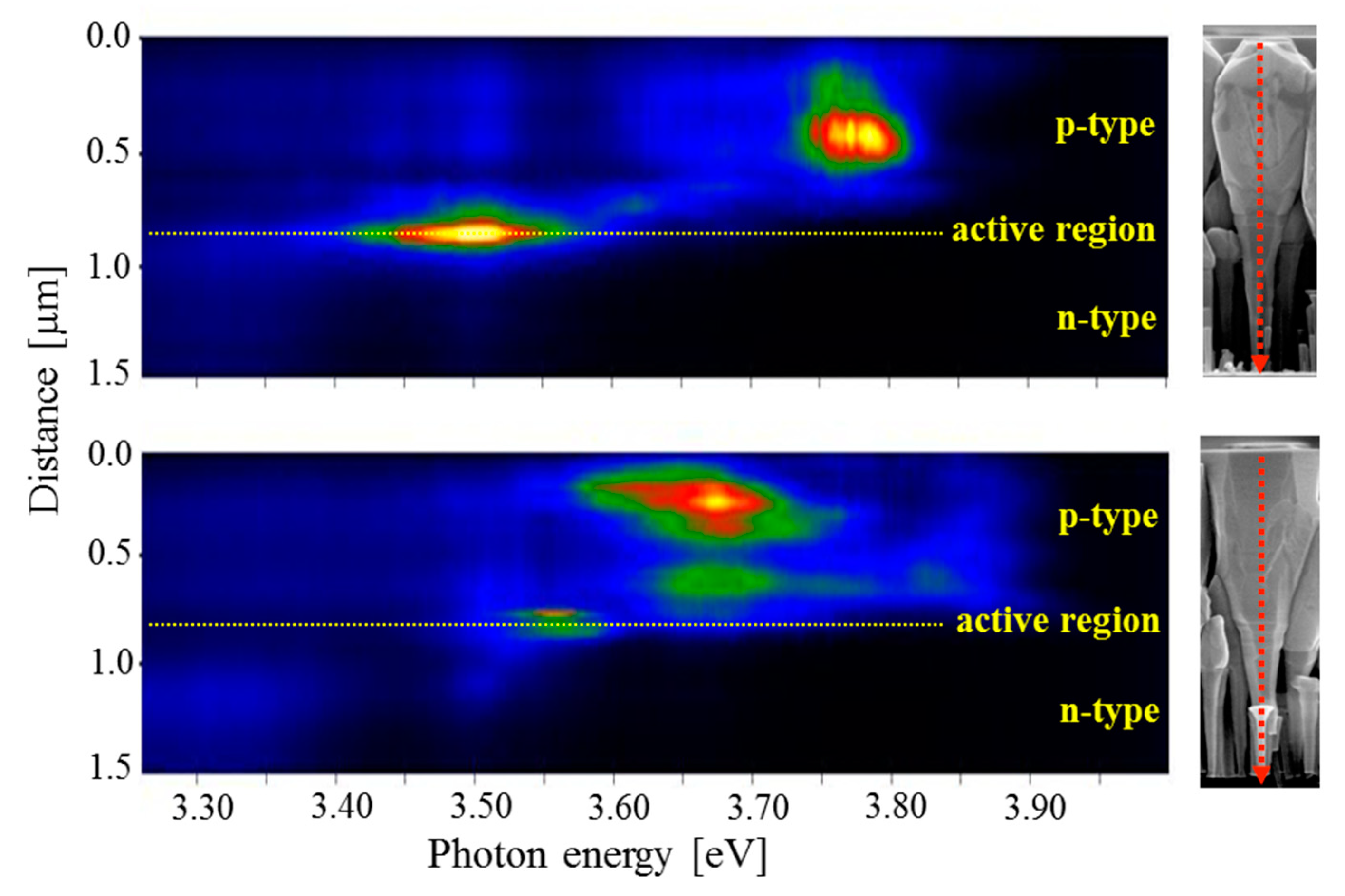
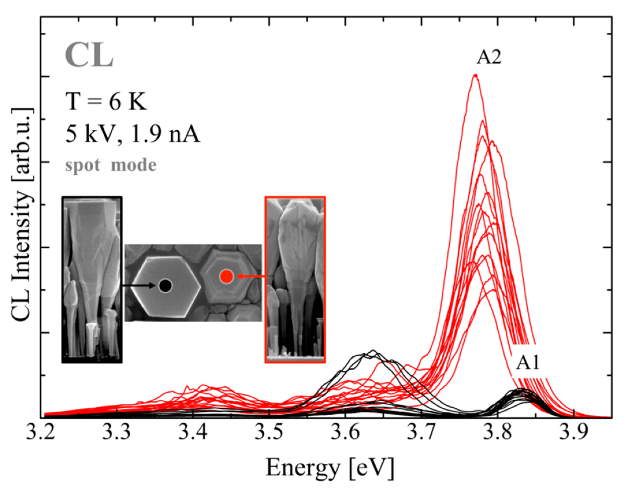
3.3.1. Cathodoluminescence Studies

SEM combined with CL enables a direct correlation of luminescence maps and sample morphologies at the nanoscale level. The high spatial and spectral resolution and high energy excitation of this method make it the perfect tool for studying the optical properties of nanostructures that emit light in the UV range [37,38,39].
NW arrays were studied by CL spectroscopy and imaging at 5 K using an acceleration voltage (AV) of 5 kV and a beam current (Ib) of 1 nA. Spectra and monochromatic CL maps were collected in the cross-sectional geometry using the photomultiplier mode. In the CL spectrum (Figure 6, central panel), four main emission bands can be distinguished. Two bands—A1: 3.83 eV; and A4: 3.63 eV—are related to AlGaN luminescence. The CL maps (Figure 6, right side) confirmed that the emission comes from the upper (p-type) part of the NWs. The presence of two bands is most probably related to the existence of inhomogeneous Al contents in AlGaN. The third emission line, G1 centered at 3.47 eV, is related to the luminescence of the QWs. The emission of QWs is clearly visible in the corresponding CL map (Figure 6, left side). The fourth one, G3 at 3.3 eV, most probably comes from the recombination of donor–acceptor pairs.
To study local optical properties in detail, CL spectrum line-scans at 5 K were recorded for a number of individual NWs (in a cross-sectional geometry) using an AV of 5 kV and Ib of 1 nA. A CCD camera in the CL line-scan mode enabled the acquisition of a series of luminescence spectra of the individual NWs, which were excited with the electron beam point-by-point along the specified line parallel to the NW axis. The direction of the line-scans is illustrated in the SEM insets shown in Figure 7. Typical results are shown in Figure 7. The set of spectra in the upper panel corresponds to the CL line-scan of the nanowire with an oval shape, where the polarity switched to the Ga-one, while the bottom panel shows the spectra for a fully N-polar hexagonal NW.
As can be seen in the upper panel in Figure 7, the bright luminescence from the active region is observed in the Ga-face NWs. Since the QWs emission is the main source of LED radiation, we conclude that a reversal of NW polarity is crucial for LED efficiency. The N-face NWs had a strong emission related to the A4 peak at 3.65 eV, which was emitted in the upper part of the NW.
A series of spectra of the individual NWs was also collected in the top-view configuration. The CL in the spot-mode was measured at 6 K using an AV of 5 kV and Ib of 1.9 nA. The electron beam parameters have been adjusted so that only the upper, p-type Al0.2Ga0.8N:Mg part of the LED NW structure was excited. A Monte Carlo simulation of the CL intensity distribution, performed using the Casino v2.48 (2.4.8.1) software [40], allowed us to estimate the size of this region. For AV = 5 kV, about 90% of the CL signal comes from a depth of 200 nm.
Observing Figure 7 and Figure 8, one can easily see that the different peaks in the CL spectra correlate with the differences in the shape of the NWs. The AlGaN:Mg emission was expected to be above 3.5 eV. The hexagonal-shaped (N-polar) NWs emissions corresponded to the A1 and A4 peaks, while the oval-shaped (Ga-polar) NWs emitted mainly at 3.78 eV (peak A2). The lower energy of the oval-shaped NWs implies that these NWs have a lower Al content. Since the Al desorption at used growth temperatures is negligible, irrespective of the polarity, this was probably caused by the higher Ga incorporation into AlGaN on the N-polar than on the Ga-polar surface, which is similar to the case of In during InGaN growth [41].

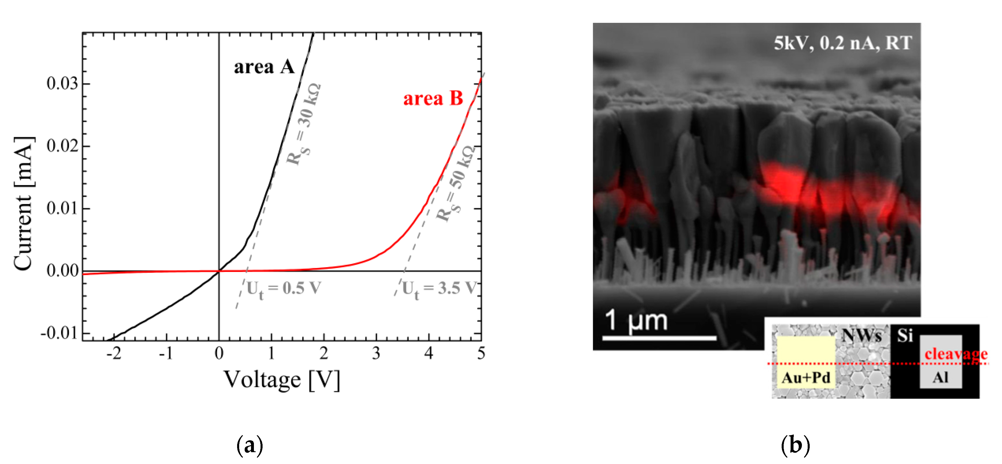
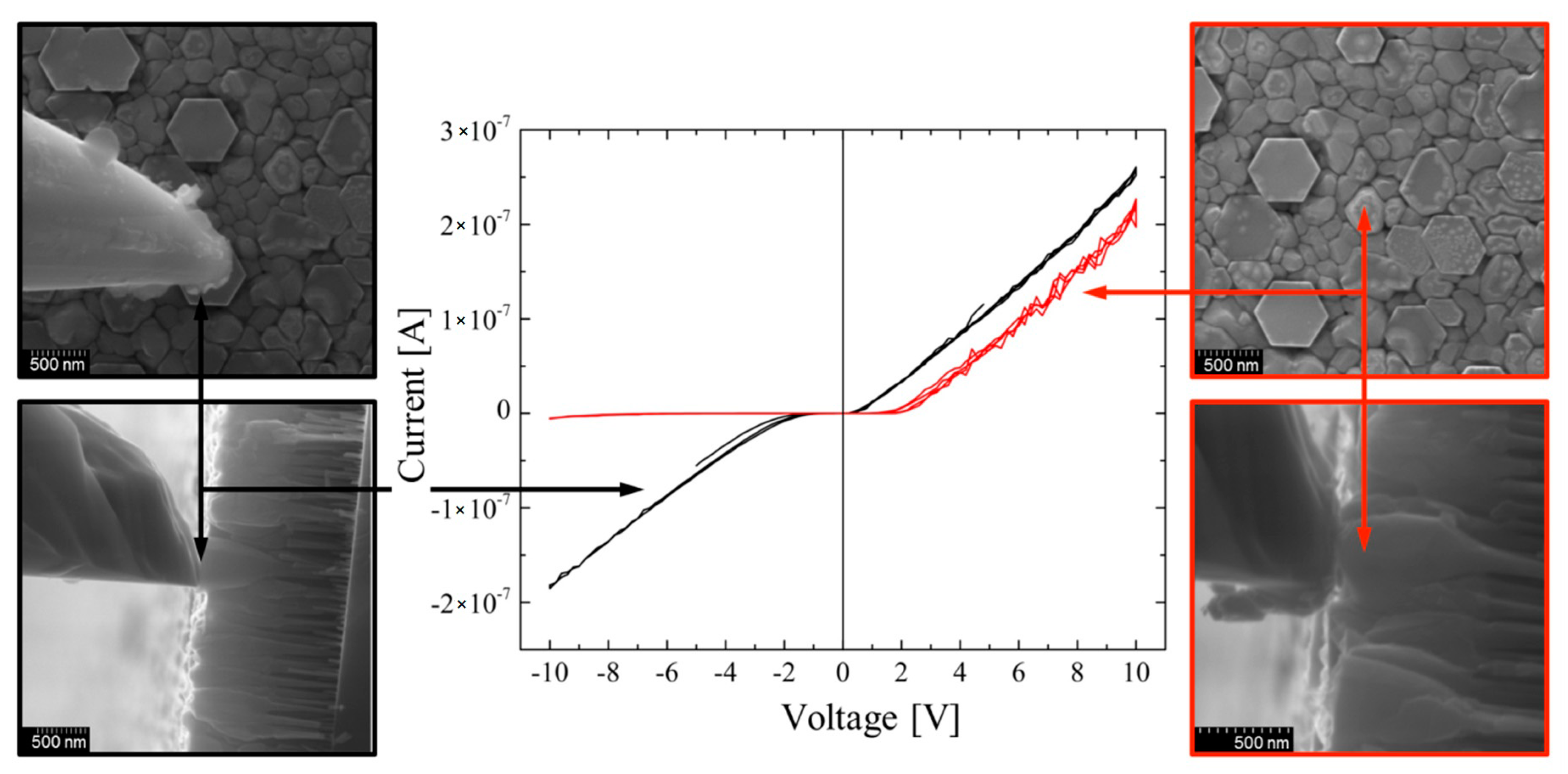
3.3.2. EBIC and Nano-Probe Results

The EBIC technique was used to assess and analyze the local electrical properties of the structure. The interaction of the electron beam with the semiconductor structure results in the generation of electron–hole pairs, which are separated in the presence of an internal field near the p–n junction. As a result, an electrical current is generated, providing the EBIC signal. This technique, combined with SEM, enabled the visualization of the position and continuity of the p–n junction and estimation of the width of the depletion region [42,43].
The electrical measurements conducted on the wafer with the NWs revealed that the NW LED structures in the central B area of the wafer exhibited diode-like I–V curves (Figure 9a), which means that we could expect a current generation caused by an electron beam. The obtained EBIC contrast image is presented in Figure 9b. EBIC measurements were performed at room temperature using an AV of 5 kV and Ib of 0.2 nA, without applying any bias voltage. The Au+Pd contact was deposited on the p-type NW tops using a sputter coater. Al contacts were deposited onto the exposed Si (n-type) substrate using the same method. The sample with deposited contacts was cleaved for EBIC measurements in the cross-sectional geometry. The EBIC contrast (red) superimposed on the SEM image (grey) revealed the position of the active part of the p–n junction. We observed a strong EBIC signal only in the NWs with the “oval-like” shape tops. The depletion region in these LED NWs was located on the side of the p-type part of the structure, and its width was about 300 nm. A Monte Carlo simulation of CL from GaN under such conditions shows that about 65% of the emission originates from a volume with a diameter of 10–15 nm. This also gives us an estimate of the lateral resolution of the EBIC experiment and confirms that it insignificantly interferes with the observed width of the depletion region [40]. This observation meant that the p-type part had a lower concentration of electrically active acceptor dopants, compared to the concentration of donors in the n-type part, even if the nominal concentration of the acceptors was ten times higher. This was due to the weak activation of Mg acceptors.
To investigate the I–V characteristics of individual LED NWs, a tungsten-tip nano-probe was used to form the top ohmic contact. The native tungsten oxide was preliminary removed from the tip using a 30 keV focused Ga+ ion beam. Thin silver wire, glued by conductive silver paste, provided the ohmic contact to the silicon substrate. The bias voltage was applied between the needle and the grounded substrate [44,45]. The current–voltage characteristics were measured for the two different types of nanowires with different shapes and polarities. The measurements were repeated on different spots of the sample, achieving a reasonable reproducibility (see Figure 10). The sharp hexagons (black curves) exhibit nonlinear, symmetrical I–V curves, with a low turn-on voltage. The NWs with the rounded edges (red curves) exhibit nonlinear and nonsymmetrical diode-like I–V curves.
Both the EBIC and nano-probe measurements revealed that the p–n junction works properly only in the NWs with the oval-like top segment and that only these NW structures act efficiently as LED diodes.

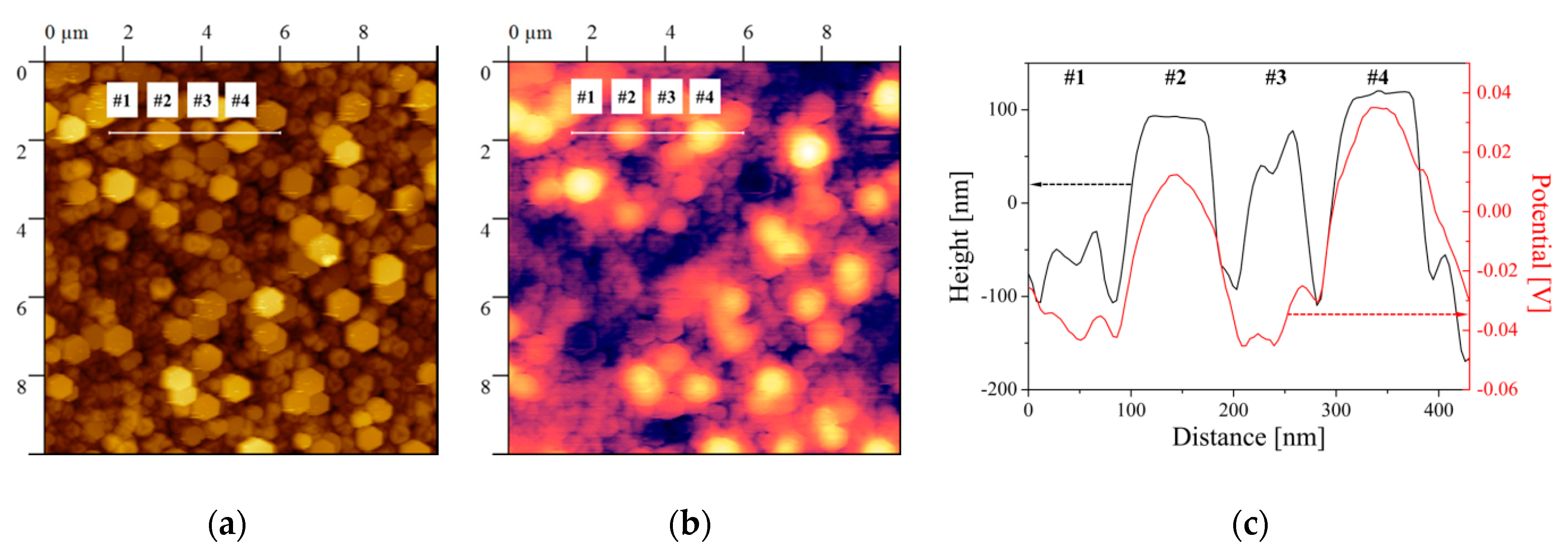
3.3.3. Kelvin Probe Force Microscopy
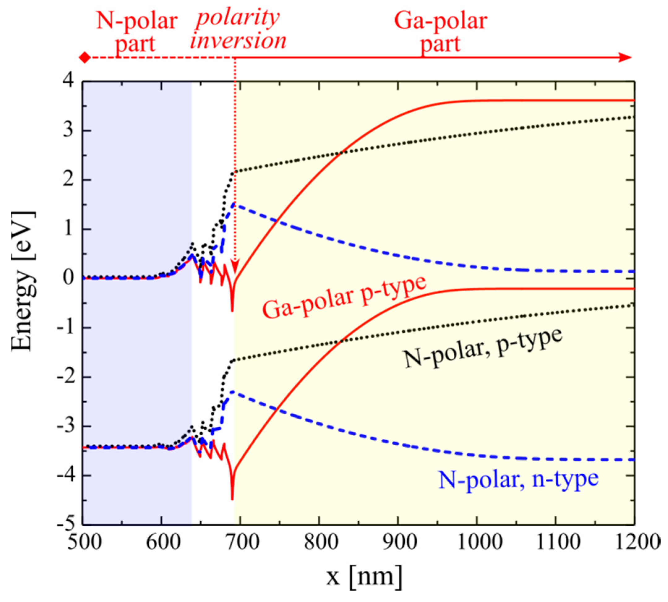
The change in the NW polarity should produce significant differences in the surface potential at the top of the NW. The surface potential profile at the microscale for individual NWs can be measured by Kelvin probe force microscopy (KPFM). The KPFM allows for the determination of the polarity of single NWs over micrometer-large surface areas with a nanometer resolution, without the need for any special sample preparation. In the KPFM studies, the local-contact potential difference (VCPD) between the metallic tip and sample was measured. By scanning the sample surface in KPFM measurements, we can compare the potentials of different wires, and local changes can be determined.
Nitrides of V-group elements, including AlGaN, exhibit a strong built-in electric field caused by spontaneous polarization, together with a piezoelectric contribution due to a strain-related electric polarization along the AlGaN axis. We assume that the potential at the wafer and along the NW up to the QW region is the same for all NWs. Then, above the QW, the polarity is reversed, so the built-in field should be different by a few MV/cm. Consequently, we expected a difference in the potential at the top of the nanowire [30]. The VCPD is expected to be higher at the N-polar than the Ga-polar surfaces. This assumption is in agreement with our calculations presented below and with earlier reports on GaN epitaxial layers [46] and nanowires [47] grown according to the MBE technique.
In the topography map (Figure 11a), the hexagonal wires appear to be higher and brighter. In the KPFM contrast (Figure 11b), still larger brightness differences between the hexagonal-shaped (N-polarity) and oval-shaped (Ga-polarity) NWs are visible. This means that the N-polar wires had a much higher electrical potential than the Ga-polar ones. In Figure 11c, the height and VCPD profiles along the line marked in Figure 11a,b through four NWs are plotted as red and black curves. The black curve denotes the height profile from the AFM topography image, in which two NWs with flat hexagonal tops—NW2 and NW4—and two NWs with rough, oval tops—NW1 and NW3—are visible. The red curve is the profile of VCPD from the KPFM contrast map. It can be seen that the surface potential is not correlated with the height of the NWs and is much higher for the NWs with flat hexagonal tops; therefore, the contrast shown in the KPFM map is not an artifact resulting from the NW topography. The results of the KPFM experiments are fully consistent with the results concerning the polarity determination, performed by KOH etching of the NWs (see Section 3.1).

4. Discussion

It is known that during the growth of catalyst-free GaN on silicon using the PAMBE technique, the N-rich conditions promote columnar growth, leading to the formation of NWs that are mainly nitrogen-polar [18,48,49,50]. In the case of our GaN/AlGaN NW LED structures, the n-type part of the structure (GaN:Si) and the active region of the structure with three QWs, which were grown under N-rich conditions, exhibit nitrogen polarity, which was confirmed for many previously grown structures. During the growth of the p-type part, to enhance the Mg incorporation and increase the NW diameter, the temperature was decreased, which promoted lateral growth. However, lowering the growth temperature increases the possibility of stacking fault formation and switching of the polarity to Ga-polar. Moreover, such conditions enabled the more efficient incorporation of Mg dopant [51]. The polarity inversion induced by Mg-doping in GaN has been observed before by many groups, but usually 2D structures were studied, and the polarity changed from Ga- to N-polar in the samples from both the MOCVD and MBE growth processes [52,53,54,55,56]. It was reported that doping of N-face GaN with Mg resulted in a crystalline phase transition from wurtzite to zinc blende [57,58]. However, switching from N- to Ga-polarity was also observed as a result of Mg-doping during PAMBE growth. In one case, it was achieved by exposing the surface of the GaN layer to Mg and N fluxes during growth interruption at a reduced substrate temperature, and the formation of a MgxNy compound was suggested to be responsible for inverting the crystal polarity [59]. In the second case, the polarity of GaN was inverted from the N- to Ga-face by inserting a composite AlN/AlOx interlayer structure at the inversion interface [60].
In wurtzite structures, the growth polarity strongly influences the incorporation of dopants and impurities and affects the formation of native point defects. Additionally, the doping behavior of Mg and resulting conductivity of the doped structures were found to be strongly dependent on the surface polarity of the growing GaN planes. In the PAMBE process, the incorporation rate of the most common dopant used for achieving p-type conductivity is significantly higher in Ga-polar structures, while N-polar growth inhibits effective Mg doping. A lower Mg incorporation efficiency in N-face GaN has been predicted theoretically [61] and confirmed experimentally [53,62,63].
Oxygen atoms are one of the most common impurities in the GaN growth process, especially if Al-containing alloys are used. Oxygen acts as a shallow donor [64,65] and compensates Mg acceptors. It was widely reported that oxygen incorporation is also dependent on the growth polarity. Oxygen can be incorporated much more easily into N-polar (Al,Ga,In)N films in comparison to metal polar films. The higher oxygen incorporation efficiency on the N-polar surface was associated with a facile exchange between N-surface atoms and oxygen [62,66,67].
In order to understand the origin of different electrical characteristics of the two types of nanowires, a set of band profiles was calculated using a one-dimensional Drift-Diffusion Poisson Schrodinger Solver [68]. For simulation purposes, for each III-nitride layer, we consider only the majority dopant (i.e., acceptor or donor) concentrations, defined as the difference between the majority and minority type of dopant. Keeping in mind that the oxygen (donor) background doping levels that are typically observed are in a range between 1 × 10¹⁶–5 × 10¹⁷ atoms/cm3, the numbers indicated below may be significantly different to those implied by the dopant fluxes introduced during growth. In Figure 12, two band profiles obtained for unbiased structures of both types of NWs are compared. The black dotted line corresponds to the fully N-polar structure with n-type doping (2 × 10¹⁸ atoms/cm3) below the MQW and p-type AlGaN:Mg (2 × 10¹⁵ atoms/cm3) above it. Such a lightly doped structure should result in an extremely thick depletion region and could be easily perturbed by other effects, such as residual oxygen contamination. The blue dashed line in Figure 12 indicates how residual oxygen, at the relatively low concentration of 1 × 10¹⁶ atoms/cm3, in the nominally p-type region changes the band profile, resulting in a lack of p–n junction in the structure. This effect could explain the lack of a rectifying characteristic in N-polar NWs, as shown in Figure 10. The last profile, represented by the red line in Figure 12, corresponds to the structure in which a p-type layer polarity inversion from N- to Ga-polar took place at the beginning, and the incorporation of 5 × 10¹⁶ atoms/cm3 of Mg started. Our calculations show that this corresponds to a depletion width of approximately 300 nm situated above the MQW region, which is in agreement with the results of the EBIC studies. The assumed difference between the Mg concentrations for the Ga- and N-polar structures was in accordance with the previously reported discrepancy between both polarities [53].
In fact, there is only a small difference in doping between the models, which are represented by the black and blue curves in Figure 12. However, as shown in Figure 12, this difference is sufficient to induce a change from a weak p-type to a weak n-type semiconductor. It is possible that some N-polar NWs are slightly p-type, some are slightly n-type, and some are insulating. We have observed that some of them are electrically conductive, such as those shown in Figure 9a and Figure 10, and some are insulating. The slightly n-type NWs have their electric fields screened at the top, which is shown as the flattening of the blue dashed curve in Figure 12. This means that this part of the NW can emit CL, which is in agreement with the observation that some N-polar NWs emitted bright luminescence from their tops. It is also worth noting that the potential on the top of the Ga-face NWs is lower than the potential of the N-face NWs, which is in agreement with the KPFM measurements.

5. Summary and Conclusions

A comprehensive dataset revealing the optical and electrical properties of individual nanoLED structures embedded in GaN/AlGaN NWs emitting EL at approximately 3.3 eV has been collected. The results were obtained by complementary SEM, TEM, CL, and EBIC spectroscopy and imaging; AFM and Kelvin probe force microscopy experiments; and I–V characteristics measurements for individual NWs using a nano-probe. Further information was acquired by studying the properties of NW ensembles using electroluminescence and time-resolved photoluminescence.
We identified two types of nanowires that differ in terms of the shape of their upper parts. KOH etching and KPFM studies show that they have different polarities. We believe that unintentional fluctuations in the conditions during the growth of the Mg-doped AlGaN part of the structure caused a reversal of the growth polarity of some NWs from the N- to Ga-face.
The interpretation of the experimental data was supported by the results of numerical simulations of the electronic band structure of individual NWs, which allowed the physical mechanisms responsible for the activation or deactivation of the p–n junctions, depending on the polarity of the last p-type part in the nanoLED structures, to be discussed.
The experimental techniques with a spatial nano-resolution allowed for the study of the correlating luminescence and electrical properties of NWs, with the growth polarity switching in the p-type AlGaN part of the NW. The CL spectra showed that the N-face NWs had emissions at the highest energy of 3.83 eV, while the Ga-face NWs energy of emissions was mainly at 3.78 eV. The lower emission energy of the Ga-polarity NWs indicated that there was a lower Al content in these NWs. This, in turn, suggested a higher Ga desorption for N-face NWs than for Ga-face NWs. The monochromatic CL maps provided clear evidence of the QW emission at about 3.5 eV at helium temperature, which is the main recombination path producing electroluminescence in nanoLEDs. We observed that only Ga-polar NWs emitted bright luminescence from QWs. This is a clear indication that switching polarity was crucial for LED efficiency. According to our calculations of the band structure of the NWs, the change in polarity induced an electric field profile that attracted carriers to the region of QWs, which is the necessary condition for bright light emission. The EBIC mapping proved that p–n junctions were not active in N-polarity NWs, while Ga-polar NWs generated a strong current when excited in the junction area. The observed depletion region was mostly on the p-type side of the junction due to the relatively weak activation of Mg acceptors. The time-resolved photoluminescence showed that the lifetime of the QW-related emission was about 1–2 ns, which proved good quality QWs. The electroluminescence experiments showed that an ensemble of the investigated nanoLED NWs was acceptable as a source of UV radiation, with an energy of about 3.3 eV.
The collected data and results of numerical simulations indicate that the intentional polarity inversion between the n- and p-type parts of NWs is a potential path towards the development of efficient nanoLED NW structures. We believe that a more effective p-type doping of AlGaN, supporting an active p–n junction, would prevail over the disadvantage of the possible creation of structural defects in the polarity inversion region.

Author Contributions

Conceptualization, K.P.K., A.R., B.J.K. and Z.R.Z.; methodology, A.R., K.P.K. and B.J.K.; software, H.T.; formal analysis, A.R., K.P.K. and H.T.; investigation, A.R., K.P.K., S.T., S.K., R.B. and U.J.; resources, M.S. and Z.R.Z.; writing—original draft preparation, A.R., K.P.K., B.J.K. and H.T.; writing—review and editing, Z.R.Z., S.T., U.J. and M.S.; visualization, A.R., K.P.K. and H.T.; supervision, K.P.K., B.J.K. and Z.R.Z.; funding acquisition, B.J.K., Z.R.Z. and H.T. All authors have read and agreed to the published version of the manuscript.

Funding

This research was partly funded by the Polish National Science Centre (NCN), Grants Nos. UMO-2016/21/B/ST5/03378 and UMO-2016/23/B/ST7/03745, by the Polish National Centre for Research and Development project PBS1/A3/1/2012 Pol-HEMT and by the Foundation for Polish Science, co-financed by the European Union under the European Regional Development Fund Homing POIR.04.04.00-00-5D5B/18-00.

Institutional Review Board Statement

Not applicable.

Informed Consent Statement

Not applicable.

Data Availability Statement

The data presented in this study are available on request from the corresponding author.

Acknowledgments

The authors would like to thank M.Sc. Kamil Klosek for his assistance in the growth of the NW structures, M.Sc. Giorgi Tchutchulashvili for his help with the SEM imaging and KOH etching of the NW LED structures, and M.Sc. Michal Sztyber for his assistance in the electro- and photo- luminescence measurements.

Conflicts of Interest

The authors declare no conflict of interest. The funders had no role in the design of the study; in the collection, analyses, or interpretation of data; in the writing of the manuscript, or in the decision to publish the results.

References

  1. Seong, T.-Y.; Han, J.; Amano, H.; Morkoc, H. III-Nitride Based Light Emitting Diodes and Applications; Springer: Dordrecht, the Netherlands, 2013; ISBN 978-94-007-5863-6. [Google Scholar]
  2. Huang, J.-J.; Kuo, H.-C.; Shen, S.-C. Nitride Semiconductor Light-Emitting Diodes (LEDs), 1st ed.; Woodhead Publishing: Sawston, UK, 2013; ISBN 9780857099303. [Google Scholar]
  3. Wong, M.S.; Nakamura, S.; DenBaars, S.P. Review—Progress in High Performance III-Nitride Micro-Light-Emitting Diodes. ECS J. Solid State Sci. Technol. 2020, 9, 015012. [Google Scholar] [CrossRef]
  4. Romualdo, A.F.; Zhu Congyong, T.A.; Hadis, M. Group III Nitrides. In Springer Handbook of Electronic and Photonic Materials; Safa, K., Capper, P., Eds.; Springer International Publishing: Berlin/Heidelberg, Germany, 2017; p. 1536. ISBN 978-3-319-48933-9. [Google Scholar]
  5. Muñoz, E.; Monroy, E.; Pau, J.L.; Calle, F.; Omnès, F.; Gibart, P. III nitrides and UV detection. J. Phys. Condens. Matter 2001, 13, 7115–7137. [Google Scholar] [CrossRef]
  6. Zou, Y.; Zhang, Y.; Hu, Y.; Gu, H. Ultraviolet Detectors Based on Wide Bandgap Semiconductor Nanowire: A Review. Sensors 2018, 18, 2072. [Google Scholar] [CrossRef] [PubMed] [Green Version]
  7. Dwiliński, R.; Doradziński, R.; Garczyński, J.; Sierzputowski, L.; Kucharski, R.; Zając, M.; Rudziński, M.; Kudrawiec, R.; Strupiński, W.; Misiewicz, J. Ammonothermal GaN substrates: Growth accomplishments and applications. Phys. Status Solidi 2011, 208, 1489–1493. [Google Scholar] [CrossRef]
  8. Hashimoto, T.; Letts, E.; Hoff, S. Current status and future prospects of ammonothermal bulk GaN growth. Sensors Mater. 2013, 25, 155–164. [Google Scholar]
  9. Łucznik, B.; Pastuszka, B.; Grzegory, I.; Boćkowski, M.; Kamler, G.; Litwin-Staszewska, E.; Porowski, S. Deposition of thick GaN layers by HVPE on the pressure grown GaN substrates. J. Cryst. Growth 2005, 281, 38–46. [Google Scholar] [CrossRef]
  10. Fujito, K.; Kubo, S.; Nagaoka, H.; Mochizuki, T.; Namita, H.; Nagao, S. Bulk GaN crystals grown by HVPE. J. Cryst. Growth 2009, 311, 3011–3014. [Google Scholar] [CrossRef]
  11. Brandt, O.; Pfüller, C.; Chèze, C.; Geelhaar, L.; Riechert, H. Sub-meV linewidth of excitonic luminescence in single GaN nanowires: Direct evidence for surface excitons. Phys. Rev. B 2010, 81, 45302. [Google Scholar] [CrossRef] [Green Version]
  12. Glas, F. Critical dimensions for the plastic relaxation of strained axial heterostructures in free-standing nanowires. Phys. Rev. B 2006, 74, 121302. [Google Scholar] [CrossRef]
  13. Carnevale, S.D.; Kent, T.F.; Phillips, P.J.; Mills, M.J.; Rajan, S.; Myers, R.C. Polarization-Induced pn Diodes in Wide-Band-Gap Nanowires with Ultraviolet Electroluminescence. Nano Lett. 2012, 12, 915–920. [Google Scholar] [CrossRef]
  14. Kent, T.F.; Carnevale, S.D.; Sarwar, A.T.M.; Phillips, P.J.; Klie, R.F.; Myers, R.C. Deep ultraviolet emitting polarization induced nanowire light emitting diodes with Alx Ga1−x N active regions. Nanotechnology 2014, 25, 455201. [Google Scholar] [CrossRef] [PubMed]
  15. Zhao, S.; Wang, R.; Chu, S.; Mi, Z. Molecular Beam Epitaxy of III-Nitride Nanowires: Emerging Applications From Deep-Ultraviolet Light Emitters and Micro-LEDs to Artificial Photosynthesis. IEEE Nanotechnol. Mag. 2019, 13, 6–16. [Google Scholar] [CrossRef]
  16. Zhao, C.; Alfaraj, N.; Chandra Subedi, R.; Liang, J.W.; Alatawi, A.A.; Alhamoud, A.A.; Ebaid, M.; Alias, M.S.; Ng, T.K.; Ooi, B.S. III-nitride nanowires on unconventional substrates: From materials to optoelectronic device applications. Prog. Quantum Electron. 2018, 61, 1–31. [Google Scholar] [CrossRef]
  17. Barrigón, E.; Heurlin, M.; Bi, Z.; Monemar, B.; Samuelson, L. Synthesis and Applications of III–V Nanowires. Chem. Rev. 2019, 119, 9170–9220. [Google Scholar] [CrossRef] [PubMed]
  18. Ristić, J.; Calleja, E.; Fernández-Garrido, S.; Cerutti, L.; Trampert, A.; Jahn, U.; Ploog, K.H. On the mechanisms of spontaneous growth of III-nitride nanocolumns by plasma-assisted molecular beam epitaxy. J. Cryst. Growth 2008, 310, 4035–4045. [Google Scholar] [CrossRef]
  19. Liu, R.; Bell, A.; Ponce, F.A.; Chen, C.Q.; Yang, J.W.; Khan, M.A. Luminescence from stacking faults in gallium nitride. Appl. Phys. Lett. 2005, 86, 31–34. [Google Scholar] [CrossRef]
  20. Korona, K.P.; Reszka, A.; Sobanska, M.; Perkowska, P.S.; Wysmołek, A.; Klosek, K.; Zytkiewicz, Z.R. Dynamics of stacking faults luminescence in GaN/Si nanowires. J. Lumin. 2014, 155. [Google Scholar] [CrossRef]
  21. Pfüller, C.; Corfdir, P.; Hauswald, C.; Flissikowski, T.; Kong, X.; Zettler, J.K.; Fernández-Garrido, S.; Doǧan, P.; Grahn, H.T.; Trampert, A.; et al. Nature of excitons bound to inversion domain boundaries: Origin of the 3.45-eV luminescence lines in spontaneously formed GaN nanowires on Si(111). Phys. Rev. B 2016, 94, 1–11. [Google Scholar] [CrossRef] [Green Version]
  22. Korona, K.P.; Zytkiewicz, Z.R.; Sobanska, M.; Sosada, F.E.; Drózdz, P.A.; Klosek, K.; Tchutchulashvili, G. Reflectance and fast polarization dynamics of a GaN/Si nanowire ensemble. J. Phys. Condens. Matter 2018, 30, 315301. [Google Scholar] [CrossRef]
  23. Tchoulfian, P.; Donatini, F.; Levy, F.; Dussaigne, A.; Ferret, P.; Pernot, J. Direct imaging of p-n junction in core-shell GaN wires. Nano Lett. 2014, 14, 3491–3498. [Google Scholar] [CrossRef] [Green Version]
  24. Ambacher, O.; Majewski, J.; Miskys, C.; Link, A.; Hermann, M.; Eickhoff, M.; Stutzmann, M.; Bernardini, F.; Fiorentini, V.; Tilak, V.; et al. Pyroelectric properties of Al(In)GaN/GaN hetero- and quantum well structures. J. Phys. Condens. Matter 2002, 14, 3399–3434. [Google Scholar] [CrossRef]
  25. Klosek, K.; Sobanska, M.; Tchutchulashvili, G.; Zytkiewicz, Z.R.; Teisseyre, H.; Klopotowski, L. Optimization of nitrogen plasma source parameters by measurements of emitted light intensity for growth of GaN by molecular beam epitaxy. Thin Solid Films 2013, 534, 107–110. [Google Scholar] [CrossRef]
  26. Binder, J.; Korona, K.P.; Wysmołek, A.; Kamińska, M.; Köhler, K.; Kirste, L.; Ambacher, O.; Zaja̧c, M.; Dwiliński, R. Dynamics of thermalization in GaInN/GaN quantum wells grown on ammonothermal GaN. J. Appl. Phys. 2013, 114, 223504. [Google Scholar] [CrossRef]
  27. Sobanska, M.; Korona, K.P.; Zytkiewicz, Z.R.; Klosek, K.; Tchutchulashvili, G. Kinetics of self-induced nucleation and optical properties of GaN nanowires grown by plasma-assisted molecular beam epitaxy on amorphous AlxOy. J. Appl. Phys. 2015, 118, 184303. [Google Scholar] [CrossRef]
  28. Wierzbicka, A.; Zytkiewicz, Z.R.; Kret, S.; Borysiuk, J.; Dluzewski, P.; Sobanska, M.; Klosek, K.; Reszka, A.; Tchutchulashvili, G.; Cabaj, A.; et al. Influence of substrate nitridation temperature on epitaxial alignment of GaN nanowires to Si(111) substrate. Nanotechnology 2013, 24, 035703. [Google Scholar] [CrossRef] [PubMed]
  29. Kolkovsky, V.; Zytkiewicz, Z.R.; Korona, K.P.; Sobanska, M.; Klosek, K. Structural, electrical, and optical characterization of coalescent p-n GaN nanowires grown by molecular beam epitaxy. J. Appl. Phys. 2015, 118, 224307. [Google Scholar] [CrossRef]
  30. Zúñiga-Pérez, J.; Consonni, V.; Lymperakis, L.; Kong, X.; Trampert, A.; Fernández-Garrido, S.; Brandt, O.; Renevier, H.; Keller, S.; Hestroffer, K.; et al. Polarity in GaN and ZnO: Theory, measurement, growth, and devices. Appl. Phys. Rev. 2016, 3, 041303. [Google Scholar] [CrossRef] [Green Version]
  31. Li, D.; Sumiya, M.; Yoshimura, K.; Suzuki, Y.; Fukuda, Y.; Fuke, S. Characteristics of the GaN Polar Surface during an Etching Process in KOH Solution. Phys. Status Solidi 2000, 180, 357–362. [Google Scholar] [CrossRef]
  32. Ng, H.M.; Parz, W.; Weimann, N.G.; Chowdhury, A. Patterning GaN Microstructures by Polarity-Selective Chemical Etching. Jpn. J. Appl. Phys. 2003, 42, L1405–L1407. [Google Scholar] [CrossRef]
  33. Hestroffer, K.; Leclere, C.; Bougerol, C.; Renevier, H.; Daudin, B. Polarity of GaN nanowires grown by plasma-assisted molecular beam epitaxy on Si(111). Phys. Rev. B 2011, 84, 245302. [Google Scholar] [CrossRef]
  34. Korona, K.P.; Wysmołek, A.; Pakuła, K.; Stȩpniewski, R.; Baranowski, J.M.; Grzegory, I.; Łucznik, B.; Wróblewski, M.; Porowski, S. Exciton region reflectance of homoepitaxial GaN layers. Appl. Phys. Lett. 1996, 69, 788–790. [Google Scholar] [CrossRef]
  35. Korona, K.P. Dynamics of excitonic recombination and interactions in homoepitaxial GaN. Phys. Rev. B Condens. Matter Mater. Phys. 2002, 65, 1–8. [Google Scholar] [CrossRef]
  36. Lefebvre, P.; Morel, A.; Gallart, M.; Taliercio, T.; Allègre, J.; Gil, B.; Mathieu, H.; Damilano, B.; Grandjean, N.; Massies, J. High internal electric field in a graded-width InGaN/GaN quantum well: Accurate determination by time-resolved photoluminescence spectroscopy. Appl. Phys. Lett. 2001, 78, 1252–1254. [Google Scholar] [CrossRef]
  37. Gustafsson, A. Nanowire-based structures for infrared to ultraviolet emitters studied by cathodoluminescence. J. Microsc. 2016, 262, 134–141. [Google Scholar] [CrossRef] [PubMed]
  38. Thonke, K.; Tischer, I.; Hocker, M.; Schirra, M.; Fujan, K.; Wiedenmann, M.; Schneider, R.; Frey, M.; Feneberg, M. Nanoscale characterisation of semiconductors by cathodoluminescence. IOP Conf. Ser. Mater. Sci. Eng. 2014, 55, 55. [Google Scholar] [CrossRef] [Green Version]
  39. Reszka, A.; Wierzbicka, A.; Sobczak, K.; Jahn, U.; Zeimer, U.; Kuchuk, A.V.; Pieniążek, A.; Sobanska, M.; Klosek, K.; Zytkiewicz, Z.R.; et al. An influence of the local strain on cathodoluminescence of GaN/Al x Ga 1−x N nanowire structures. J. Appl. Phys. 2016, 120, 194304. [Google Scholar] [CrossRef]
  40. Drouin, D.; Couture, A.R.; Joly, D.; Tastet, X.; Aimez, V.; Gauvin, R. CASINO V2.42—A Fast and Easy-to-use Modeling Tool for Scanning Electron Microscopy and Microanalysis Users. Scanning 2007, 29, 92–101. [Google Scholar] [CrossRef]
  41. Keller, S.; Fichtenbaum, N.A.; Furukawa, M.; Speck, J.S.; Denbaars, S.P.; Mishra, U.K. Growth and characterization of N-polar InGaNGaN multiquantum wells. Appl. Phys. Lett. 2007, 90, 1–4. [Google Scholar] [CrossRef]
  42. Rigutti, L.; Tchernycheva, M. Electrical and Electro-Optical Characterization of Semiconductor Nanowires, 2nd ed.; Elsevier: Amsterdam, The Netherlands, 2013; ISBN 9780444595515. [Google Scholar]
  43. Tchernycheva, M.; Neplokh, V.; Zhang, H.; Lavenus, P.; Rigutti, L.; Bayle, F.; Julien, F.H.; Babichev, A.; Jacopin, G.; Largeau, L.; et al. Core-shell InGaN/GaN nanowire light emitting diodes analyzed by electron beam induced current microscopy and cathodoluminescence mapping. Nanoscale 2015, 7, 11692–11701. [Google Scholar] [CrossRef] [Green Version]
  44. Tiagulskyi, S.; Yatskiv, R.; Faitová, H.; Kučerová, Š.; Vaniš, J.; Grym, J. Electrical properties of nanoscale p-n heterojunctions formed between a single ZnO nanorod and GaN substrate. Mater. Sci. Semicond. Process. 2020, 107, 104808. [Google Scholar] [CrossRef]
  45. Tiagulskyi, S.; Yatskiv, R.; Faitová, H.; Kučerová, Š.; Roesel, D.; Vaniš, J.; Grym, J.; Veselý, J. Highly Rectifying Heterojunctions Formed by Annealed ZnO Nanorods on GaN Substrates. Nanomaterials 2020, 10, 508. [Google Scholar] [CrossRef] [PubMed] [Green Version]
  46. Rodriguez, B.J.; Yang, W.-C.; Nemanich, R.J.; Gruverman, A. Scanning probe investigation of surface charge and surface potential of GaN-based heterostructures. Appl. Phys. Lett. 2005, 86, 112115. [Google Scholar] [CrossRef] [Green Version]
  47. Minj, A.; Cros, A.; Garro, N.; Colchero, J.; Auzelle, T.; Daudin, B. Assessment of Polarity in GaN Self-Assembled Nanowires by Electrical Force Microscopy. Nano Lett. 2015, 15, 6770–6776. [Google Scholar] [CrossRef] [PubMed]
  48. Li, S.; Waag, A. GaN based nanorods for solid state lighting. J. Appl. Phys. 2012, 111, 071101. [Google Scholar] [CrossRef]
  49. Wang, Z.T.; Yamada-Takamura, Y.; Fujikawa, Y.; Sakurai, T.; Xue, Q.K. Atomistic study of GaN surface grown on Si(111). Appl. Phys. Lett. 2005, 87, 032110. [Google Scholar] [CrossRef]
  50. Calarco, R.; Meijers, R.J.; Debnath, R.K.; Stoical, T.; Sutter, E.; Lüth, H. Nucleation and growth of GaN nanowires on Si(111) performed by molecular beam epitaxy. Nano Lett. 2007, 7, 2248–2251. [Google Scholar] [CrossRef]
  51. Bhattacharyya, A.; Li, W.; Cabalu, J.; Moustakas, T.D.; Smith, D.J.; Hervig, R.L. Efficient p -type doping of GaN films by plasma-assisted molecular beam epitaxy. Appl. Phys. Lett. 2004, 85, 4956–4958. [Google Scholar] [CrossRef]
  52. Ramachandran, V.; Feenstra, R.M.; Sarney, W.L.; Salamanca-Riba, L.; Northrup, J.E.; Romano, L.T.; Greve, D.W. Inversion of wurtzite GaN(0001) by exposure to magnesium. Appl. Phys. Lett. 1999, 75, 808–810. [Google Scholar] [CrossRef] [Green Version]
  53. Ptak, A.J.; Myers, T.H.; Romano, L.T.; Van De Walle, C.G.; Northrup, J.E. Magnesium incorporation in GaN grown by molecular-beam epitaxy. Appl. Phys. Lett. 2001, 78, 285–287. [Google Scholar] [CrossRef]
  54. Keller, S.; Dora, Y.; Wu, F.; Chen, X.; Chowdury, S.; Denbaars, S.P.; Speck, J.S.; Mishra, U.K. Properties of N-polar GaN films and AlGaN/GaN heterostructures grown on (111) silicon by metal organic chemical vapor deposition. Appl. Phys. Lett. 2010, 97, 1–4. [Google Scholar] [CrossRef]
  55. Romano, L.T.; Northrup, J.E.; Ptak, A.J.; Myers, T.H. Faceted inversion domain boundary in GaN films doped with Mg. Appl. Phys. Lett. 2000, 77, 2479–2481. [Google Scholar] [CrossRef]
  56. Green, D.S.; Haus, E.; Wu, F.; Chen, L.; Mishra, U.K.; Speck, J.S. Polarity control during molecular beam epitaxy growth of Mg-doped GaN. J. Vac. Sci. Technol. B Microelectron. Nanom. Struct. 2003, 21, 1804. [Google Scholar] [CrossRef] [Green Version]
  57. Monroy, E.; Hermann, M.; Sarigiannidou, E.; Andreev, T.; Holliger, P.; Monnoye, S.; Mank, H.; Daudin, B.; Eickhoff, M. Polytype transition of N-face GaN:Mg from wurtzite to zinc-blende. J. Appl. Phys. 2004, 96, 3709–3715. [Google Scholar] [CrossRef]
  58. Sarigiannidou, E.; Monroy, E.; Hermann, M.; Andreev, T.; Holliger, P.; Monnoye, S.; Mank, H.; Daudin, B.; Eickhoff, M. Phase transition by Mg doping of N-face polarity GaN. Phys. Status Solidi C Conf. 2005, 2, 2216–2219. [Google Scholar] [CrossRef]
  59. Wong, M.H.; Wu, F.; Mates, T.E.; Speck, J.S.; Mishra, U.K. Polarity inversion of N-face GaN by plasma-assisted molecular beam epitaxy. J. Appl. Phys. 2008, 104, 093710. [Google Scholar] [CrossRef]
  60. Wong, M.H.; Wu, F.; Speck, J.S.; Mishra, U.K. Polarity inversion of N-face GaN using an aluminum oxide interlayer. J. Appl. Phys. 2010, 108, 123710. [Google Scholar] [CrossRef]
  61. Sun, Q.; Selloni, A.; Myers, T.H.; Doolittle, W.A. Energetics of Mg incorporation at GaN(0001) and GaN (000 1 - ) surfaces. Phys. Rev. B Condens. Matter Mater. Phys. 2006, 73, 1–9. [Google Scholar] [CrossRef]
  62. Li, L.K.; Jurkovic, M.J.; Wang, W.I.; Van Hove, J.M.; Chow, P.P. Surface polarity dependence of Mg doping in GaN grown by molecular-beam epitaxy. Appl. Phys. Lett. 2000, 76, 1740–1742. [Google Scholar] [CrossRef]
  63. Marini, J.; Mahaboob, I.; Hogan, K.; Novak, S.; Bell, L.D.; Shahedipour-Sandvik, F. Mg Incorporation Efficiency in Pulsed MOCVD of N-Polar GaN:Mg. J. Electron. Mater. 2017, 46, 5820–5826. [Google Scholar] [CrossRef]
  64. Zywietz, T.K.; Neugebauer, J.; Scheffler, M. The adsorption of oxygen at GaN surfaces. Appl. Phys. Lett. 1999, 74, 1695–1697. [Google Scholar] [CrossRef] [Green Version]
  65. Wetzel, C.; Suski, T.; Ager, J.W.; Weber, E.R.; Haller, E.E.; Fischer, S.; Meyer, B.K.; Molnar, R.J.; Perlin, P. Pressure induced deep gap state of oxygen in GaN. Phys. Rev. Lett. 1997, 78, 3923–3926. [Google Scholar] [CrossRef]
  66. Sumiya, M.; Yoshimura, K.; Ohtsuka, K.; Fuke, S. Dependence of impurity incorporation on the polar direction of GaN film growth. Appl. Phys. Lett. 2000, 76, 2098–2100. [Google Scholar] [CrossRef]
  67. Stolyarchuk, N.; Markurt, T.; Courville, A.; March, K.; Zúñiga-Pérez, J.; Vennéguès, P.; Albrecht, M. Intentional polarity conversion of AlN epitaxial layers by oxygen. Sci. Rep. 2018, 8, 14111. [Google Scholar] [CrossRef] [PubMed]
  68. Wu, Y.-R.; Singh, M.; Singh, J. Gate leakage suppression and contact engineering in nitride heterostructures. J. Appl. Phys. 2003, 94, 5826–5831. [Google Scholar] [CrossRef] [Green Version]
Figure 1. Scanning electron microscopy (SEM) image and scheme of the light emitting diode (LED) nanowire structure, which consists of: a GaN:Si n-type part on the bottom, an active region, which starts with AlGaN segments with an increasing Al content (3%, 6%, 9% and 12%), followed by 3 GaN quantum wells (QWs), which are sandwiched between the Al0.15Ga0.85N barriers and the p-type Al0.2Ga0.8N:Mg top.
Electronics 10 00045 g001
Figure 2. Cross-section SEM and Z-contrast scanning transmission mode (STEM) (inset) images (a) and plane-view SEM images (b) of the LED NWs. Two types of NWs can be easy distinguished: those with flat sides and hexagonal tops with sharp edges, and those which are “oval-like”, with less regular, rough tops and rounded edges. Due to the temperature gradient across the substrate, the ratio of these two types varied. Two types coexist in area A, while in area B, NWs with rounded tops are mainly present.
Electronics 10 00045 g002
Figure 3. SEM images in the plane-view of the same NW array, before (a) and after (b) KOH treatment. Before KOH treatment, two kinds of NWs—those with flat hexagonal tops and those with rounded edges—were visible. After etching, the hexagonal ones disappeared, while the oval-top NWs remained untouched.
Electronics 10 00045 g003
Figure 4. Luminescence spectra at room temperature: PL at different points in the sample (upper panel) and EL at different voltages (bottom panel). It can be observed that the GaN-related G1 peak is much stronger in area A. However, in area B, it was possible to obtain EL, which was dominated by the G1 peak.
Electronics 10 00045 g004
Figure 5. Time-resolved photoluminescence spectra in area A (a) and B (b) at T = 300 K (upper panels) and T = 4 K (bottom panels). The GaN emission can be seen in the 3.3–3.5 eV range, and that of AlGaN can be observed in the 3.6–3.8 eV range. The lifetimes at a low temperature are visibly longer. It can be noticed that the AlGaN emission decays faster than the GaN emission. In area A, GaN PL has a longer lifetime.
Electronics 10 00045 g005
Figure 6. Cathodoluminescence spectrum of the NW array (central panel) and corresponding monochromatic CL maps superimposed with SEM images (sides), collected in the cross-sectional mode. Two bands—A1: 3.83 eV; and A4: 3.63 eV—are related to AlGaN luminescence. In the corresponding CL maps (right side), the emission is visible in the upper (p-type) part of the NWs. The third emission line, G1 centered at 3.47 eV, is related to the luminescence of the QWs, which proves the corresponding CL map (left side). The fourth one, G3 at 3.3 eV, most probably comes from the recombination of donor–acceptor pairs.
Electronics 10 00045 g006
Figure 7. CL line-scans collected along the individual NWs: upper panel—scan along the oval-like NW; bottom panel—scan along the hexagonal one. The bright emission from the active region is observed in the Ga-face NWs. The N-face NWs had a strong emission related to the A4 peak at 3.65 eV, which was emitted in the upper part of the NW. The arrows on the SEM images indicate the direction of the scans.
Electronics 10 00045 g007
Figure 8. Series of cathodoluminescence spectra collected in the spot-mode using AV = 5 kV, where only the top (p-type) part of the structure is excited. Differences between NWs with flat hexagonal tops (black curves) and irregular ones (red curves) are clearly visible. The inset shows the geometry of the measurements.
Electronics 10 00045 g008
Figure 9. (a) Macroscopic I–V curves of the A and B areas of the wafer. Lines fitted to the curves show serial resistance deduced from the slope and turn-on voltage deduced from the crossing with the zero axis. (b) SEM image (grey) with the superimposed EBIC signal (red) of the LED NWs. The strong EBIC signal reveals the position of the active p–n junction. The inset shows the geometry of the contacts.
Electronics 10 00045 g009
Figure 10. Series of I–V curves (central panel) of individual nanowires (NWs) (black curves: hexagonal top NWs; red curves: irregular NWs) and corresponding SEM images, showing the geometry of the measurements (sides). The sharp hexagons (black curves) exhibit nonlinear, symmetrical I–V curves with a low turn-on voltage, while the NWs with rounded edges (red curves) exhibit nonlinear and nonsymmetrical diode-like I–V curves.
Electronics 10 00045 g010
Figure 11. (a) Atomic Force Microscopy (AFM) topography (color scale from 0−500 nm), (b) the Kelvin probe force microscopy (KPFM) contrast map (color scale from 0−0.2 V), and (c) line-scan profiles of the height (in black) and potential on the surface (in red) through four NWs.
Electronics 10 00045 g011
Figure 12. Conduction and valence band profiles for three different nanowire structures, as a function of the location in the wire. The growth direction goes from left to right. The dotted black line denotes the profile for a lightly doped N-polar structure, with a 2 × 10¹⁵ atoms/cm3 Mg concentration. The dashed blue line denotes the profile for the case in which oxygen compensated p-type doping, resulting in n-type doping. The red profile corresponds to the structure in which polarity inversion took place right at the beginning of the p-type layers. The dotted arrow indicates the position where polarity inversion took place for the wire presented in red. From that moment, the structure was Ga-polar, with a 5 × 10¹⁶ atoms/cm3 Mg concentration. The vertical axis shows the electron energy E = −eΦ, where Φ is the potential.
Electronics 10 00045 g012
Publisher’s Note: MDPI stays neutral with regard to jurisdictional claims in published maps and institutional affiliations.

