Abstract
Network-on-chip (NoC) based system-on-chips (SoC) has been a promising paradigm of core-based systems. It is difficult and challenging to test the individual Intellectual property IP cores of SoC with the constraints of test time and test power. By reusing the on-chip communication network of NoC for the testing of different cores in SoC, the test time and test cost can be reduced effectively. In this paper, we have proposed a power-aware test scheduling by reusing existing on-chip communication network. On-chip test clock frequencies are used for power efficient test scheduling. In this paper, an integer linear programming (ILP) model is proposed. This model assigns different frequencies to the NoC cores in such a way that it reduces the test time without crossing the power budget. Experimental results on the ITC’02 benchmark SoCs show that the proposed ILP method gives up to 50% reduction in test time compared to the existing method.
1. Introduction
Considering time-to-market, today’s system-on-chips (SoCs) are becoming sea-of-cores! The overall architecture of SoC is becoming complex. In this scenario, testing of each IP core as stand- alone and as a part of system is difficult. Test access mechanism (TAM) architecture is designed to fetch the test data from the automatic test equipment (ATE) to the core and to transfer test response from the core to sink. The bus-based TAM was being widely used in SoC. The typical bus-based TAM architecture for SoC is having blems related to scalable global synchronous clock, communication time and performance issues [1]. To overcome these issues, NoC based SoCs are introduced. Use of routers, channels and packet switching interconnections reduces the problem of test data communication from source to IP core and IP core to sink [2].
For effective reduction in test time under the constraints of power budget, test scheduling is the key point [3]. Minimization of test time with NoC being used as TAM is a multivariable problem, including the co-optimization of the core assignment to TAM for test data transportation, active exploitation of the channel bandwidth, and the number and location of the test interface. Further, it is to be noted that the test time and test power are correlated issues. Increase in test frequency may reduce the test time but simultaneously increases the dynamic test power. In this paper, an ILP based method is proposed to reduce the test time in NoC with multiple test clock frequencies. Here, the test power and the test time are formulated as a function of the test clock frequency, and hence this method gets the test time reduction for the predefined power limit. In the proposed method, dynamic clock control based on the power dissipation of the test session is adopted.
The whole paper is organized as follows. Section 2 discusses the prior work on TAM in NoC. The motivation and background are described in Section 3. The problem statement is described in Section 4. The proposed test methodology to establish the problem statement is shown in Section 5, whereas Section 6 discusses the experimental result analysis. Finally, Section 7 draws a conclusion.
2. Prior Work
TAM architecture is the mediator to transfer the test data from automatic test equipment to the core and the core to the sink. In NoC based SoC, the NoC fabric can be used as TAM replacing the dedicated TAM. Since no extra hardware is required to build TAM, it reduces the cost of NoC based SoC testing. The fundamental of reusing NoC as TAM is first introduced in [3]. Here, the core having a longer test time is given higher priority in scheduling to reduce testing time. This method was further developed in [4], with power constraint and increased test parallelism. In [5], the test time has been shown as a function of the TAM width and assignment of a core to the TAM width to minimize the test time. In [6], it is shown that the test time of the core varies in staircase pattern with TAM width.
For high speed data transport over the network, the time division multiplexing (TDM) approach was discussed in [7]. In [8,9], power-aware test scheduling is shown by effectively utilizing the on-chip network. Here the on-chip clocking is used in such a way that the faster clock is assigned to some cores and slower to remaining to limit the overall power consumption. In short, clock rate distribution is effectively designed in this methodology to have a lower test time. Test scheduling using rectangle packing solution and use of multiple test clocks for NoC test was proposed in [10]. Test scheduling with the different topology of the network was described in [11]. In [12], unicast-based multicast scheme is used for NoC based SoC testing, where different techniques like test data compression, power constraint scheduling, vector compactions are also combined to minimize test time. Power and thermal-aware NoC test scheduling with a multiple clock rate is proposed in [13]. The algorithm is designed based on Integer linear programming and simulated annealing technique. Co-optimization of pin assignment to the access point and NoC core test scheduling was proposed in [14]. Minimization of test time with the given pin count is well described here. In [15], test delivery optimization of many core systems is proposed. Here, NoC partitioning difficulty is formulated with dynamic programming. In [16], the hybrid test data transportation system for advanced NoC based SoC is described. As the schedule is affected by the location of the access point and the position of the embedded core, a new technique is developed here for concurrently testing several different cores.
3. Motivation
The ITC’02 benchmark NoC based SoC d695 was used as an example. The d695 has 10 IP cores with 2D mess topology, as shown in Figure 1a [4]. The IP cores included in d695 are standard ISCAS benchmark circuits. The database for the SoC d695 is shown in Figure 1b, which includes number of I/Os, scan chain, number of test patterns, test power and test time [17,18].
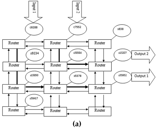
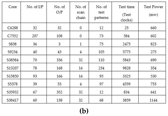
Figure 1.
(a) ITC’02 Benchmark circuit for NoC based system-on-chips (SoC)—d695 [4] (b) SoC d695 database [17,18].
Here, there are 10 cores each with test time ti and power dissipation Pi. The cores can be tested individually or in groups i.e., sessions. The length of each session i.e., test time for that session can be defined as the maximum of test time of individual core being tested in that session and total power dissipation for that session is the summation of individual test power of cores being tested in that session.
Generally, the available NoC channel width exceeds the TAM width of IP core test wrapper and hence some channel width may remain idle during testing. If we assign the cores to channel in such a way that, parallel testing of core is maximum and the idle channel width is minimum, then the test time is reduced effectively. In [19], we have presented the algorithm for the effective utilization of idle channel width to determine the width of the TAM bus assigned to the individual core and improved partition strategy for the TAM bus. The algorithm also focuses on improved core assignment to the partitioned TAM bus and test scheduling. The limitation of the algorithm in [19] is that it is exhaustive in nature and has a long execution time for big SoCs.
Here, in Figure 2, we show the effective TAM and IO assignment for the test scheduling of SoC d695 cores without power constraints. The number in each rectangle block represents the core number and corresponding test time in terms of test clock cycles for that core. The shaded region in this figure shows the idle time. Cores are mapped to any one of the three I/O pair. Results show that cores 1, 2, 7, 8 and 10 are assigned to IO1, cores 3 and 6 are assigned to IO2, and cores 4, 5 and 9 are assigned to IO3. Total test time of the cores assigned to IO1 is 12,352 clocks, total test time of the cores assigned to IO2 is 12,303 clocks and total test time of the cores assigned to IO3 is 12,452 clocks. In short, total test time of the SoC d695 is the maximum out of these three, which is 12,452 clocks.
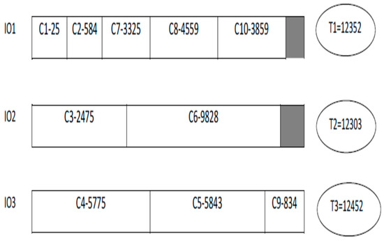
Figure 2.
Test scheduling with effective test access mechanism (TAM) width allocation.
With single frequency allocation, assuming a normalized test frequency of 1Hz in Figure 2a, maximum test time out of three I/O pair is 12,452 s.
In [20], we have proposed a method to minimize the test time in NoC based SoC by variable clock frequency to session based scheduling. Let’s assume that the maximum allowable average power for SoC is Pmax and test power for individual core is Pcore, and test frequency is ftest. Here test time is inversely proportional to test frequency and dynamic test power is directly proportional to test frequency. Hence to reduce an individual core’s test time, we have increased its test frequency by a power factor time. The power factor was considered based on the power limit constraint of SoC. Power Factor = Pmax/Pcore. After increasing the test frequency, the scheduling/rectangle packing of IP core is converted into serial testing of cores. With experimental results on different benchmark SoCs, we have shown that the overall test time was reduced for each SoC. But the limitation here is reliability issues. As we have made each of the core to run at higher frequencies, the thermal reliability issues were still unanswered.
Here, in this paper, to overcome the limitation of reliability issues, we have adopted a power constraint test scheduling where the maximum power limit was set as the percentage of the gross of total functional power consumption of all core i.e., 30% power means 30% of summation of total power consumed by each core. This value of 30% was chosen to stringent the power constraints for our experiments [9]. We have further constrained the frequency to increase by factor two for some of the cores with lower power budget and at the same time the frequency is slow down by factor ½. With higher power budget cores. In general, we used ftest, 2ftest or 1/2 ftest to individual cores using Pmax and Pcore as constraint values.
Figure 3a,b shows the test scheduling of SoC d695 cores with power constraints. Here, Pmax value is taken as 30% of the total test power consumed by all cores in SoC. Number in each rectangle block represents core number and corresponding test clock cycles of that core. Cores are mapped to any one of the three I/O pair.
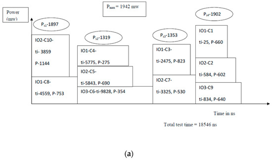
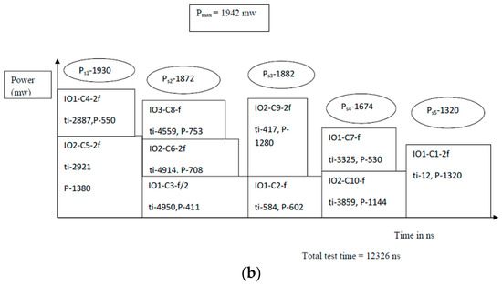
Figure 3.
(a) Power aware test scheduling with single frequency allocation (b) Power aware test scheduling with multiple frequency allocation.
With single frequency allocation in Figure 3a, the maximum test time out of three I/O pair was 18,546 ns (considering a normalized test frequency of 1GHz) whereas, with multiple frequencies in Figure 3b, it was 12,439 ns considering the three clock frequencies ½ GHz, 1 GHz and 2 GHz, which showed the reduction in test time.
Further, we have used the TAM channel width and IP core’s bus width as constraint for scheduling. It means, the test time reduction problem formation was done using the integer linear program where the TAM channel width, IP core’s bus width, Pmax and Pcore were used as a constraint for scheduling and frequency allocation objective. The exact problem formation for ILP is described in the next section.
4. Problem Statement
The problem statement for the proposed method of test time minimization can be stated as below:
- Given the number of inputs, outputs and scan chains for the NoC based SoC;
- Given the maximum TAM width Wmax to be used for data transfer between IP cores of SoC;
- Given the network topology for NoC to be used for IP cores of SoC;
- Given the multiple test clock frequency for the testing of various IP Cores in NoC based SoC;
Determine:
- Optimum allocation of the core to the input-output pairs.
- Optimum allocation of test clock to the cores.
- Scheduling algorithm to minimize test time with given power constraints.
5. Proposed Methodology
Here, ILP based test scheduling algorithm is proposed for a dedicated routing path, which is implemented for the non-preemptive test.
The ILP based schedule will assign each core a dedicated routing path, input port, output port, test clock frequency, channel through which test vector will transport from input port to the core and output response from core to the output port. Once the core is scheduled in the dedicated routing path, all the resources are reserved until entire test is finished for that core.
Let us consider:
- Nc = Number of Cores;
- Np = Number of input-output pairs available in NoC based SoC;
- Wmax = a maximum TAM width;
- ti = test time of core i;
- fn = multiple test clock frequencies.
- T = total test time
- Tro = time consumed in the router
- Tchan = time consumed in NoC channels
- Nchan = number of channels
- Nro = the number of routers
- Pro = power consumed in the router
- Pchan = power consumed in NoC channels
- Nchan = number of channels
- Nro = number of routers
- Si = length of wrapper-scan-in chain
- So = length of wrapper-scan-out chain
- TP = Test pattern count of the core
Here we are considering mesh network as the network topology for IP Cores of NoC based SoC.
The test time ti of the core i is the combination of the two entities.
(1) The time it takes to transmit data through a number of channels and routers, which is defined as Tcri
(2) Test time of the core which is defined as Tcorei
Core test time Tci depends on the TAM width selection and arrangement of the scan chain with the best fit decreasing algorithm [17]. So total core test time in terms of clock cycles is given as
The combined test time of the SoC can be defined as
In NoC, the testing time of core is considerably higher than the transmit time. So here, the transmit time is neglected as in contrast to core test time. Here, Si and So is basically a wrapper scan in and scan out flip flops and it works on the edge of clocks, so the test time measured here is in the number of clock cycles it used.
The scheduling of the core will start after calculating test time of each core. Here, we are proposing two scheduling techniques: 1. test scheduling without power constraint; 2. test scheduling with power constraint. ILP formulation is developed to schedule the cores. We will discuss and analyze these two techniques here.
(3) ILP formulation for Test Scheduling with single frequency allocation and without power constraint:
The main motive behind this algorithm is to reduce test time of the SoC. So, the main objective for this ILP formulation becomes the minimization of test time.
Main Objective: Min T
Let Xij is the 0-1 binary variable which is defined as
Each core is mapped to one and only one input-output pair. Mathematically, we can write this unity condition using the binary variable Xij, which is defined as
Since test time of SoC is maximum of individual I/O pair’s test time. The maximum test time among all I/O pairs can be given as
(4) Pseudo Code for the ILP Problem formulation
The detail description of ILP formulation in form of pseudo code is shown in Figure 4.
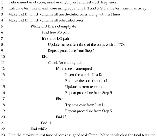
Figure 4.
Pseudo code for ILP problem formulation.
(5) Power aware test scheduling with multiple frequency allocation.
In NoC, power consumed in routers and channels is given as
Power consumption in each core can be calculated from information, like the number of input-outputs, a number of scan flip flops etc. So total power consumption can be given as,
Power aware test scheduling starts with Equation (6) and (7). Here, Cores are scheduled in such a way that power consumption in a given session should not go beyond Pmax value. Mathematically it is defined as:
where, S is the number of sessions.
Since test time of SoC is the maximum of individual I/O pair’s test time. The maximum test time among all i/o pairs can be given as
The ILP model of this whole system can be summarized as
Objective: Minimize ‘T’ Subject to:
The detail description of ILP formulation in form of pseudo code is shown in Figure 5.
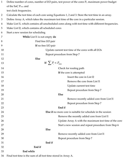
Figure 5.
Pseudo code for Proposed ILP Problem for Power aware test scheduling with Variable Test Frequency Allocation.
6. Experimental Results and Analysis
Here, the proposed algorithm was implemented on the windows core i3 processor with 2.00 GHz frequency and 4 GB RAM. The simulation was done on MATLAB 14 and LPSOLVE. The algorithm was applied to the widely used ITC’02 benchmark SoCs. Since the power consumption of each core is not mentioned in the ITC’02 benchmark database, it was taken from [21]. For the proposed algorithm, it was assumed that SoCs have the similar NoC fabric as given in [9,15,17] including network topology, core placement etc.
The simulation results of the proposed algorithm for various SoCs were compared with [9,17]. Table 1 and Table 2 show the detailed results for ITC’02 benchmark SoC d695. Columns 2–3 in Table 1 show the results in case of normal algorithm and ILP based Algorithm implementation with two cases:

Table 1.
Results of test scheduling with single frequency allocation and without power constraint for SoC d695 using integer linear programming (ILP).
Table 2.
Proposed clock allocation & core scheduling in case of multiple frequency allocation without power constraint using ILP.
- Single frequency allocation: where the normal test frequency is applied to each core and then test scheduling is done.
- Multiple frequency allocation: each core is mapped with any one of f/2, f, and 2f frequency and then power constrained test scheduling is done.
Frequency allocation was done with the ILP model as described earlier. Results are shown in Table 2, which describes the allocation of frequencies to different cores and allocation of cores to I/O pairs. Column 1 shows the number of I/O pairs for each system. Column 2 shows the mapping of the core to different I/O pairs and allocation of frequency to the core. For example, for I/O pair 2/2, cores 3, 4, 6 and 9 are assigned to I/O pair 1 and cores 1, 2, 5, 7, 8 and 10 are assigned to I/O pair 2. It also shows the allocation of frequency to the cores. For example, Core1-f/2 means core1 is assigned with frequency f/2. Similarly, all the cores are assigned with a specific frequency. Optimized results of test time are shown in the last column of that table.
Table 3.
Comparison of the proposed test scheduling results with preceding work [9] for SoC d695.
Table 4.
Comparison of proposed test scheduling results with preceding work [9] for SoC p22810.
Table 5.
Comparison of proposed test scheduling results with preceding work [9] for SoC p93791.
7. Conclusions
Here, it is shown that significant test time reduction is achieved by mapping the appropriate test clock frequency to the core with power constraint test scheduling. Here, the dedicated routing path algorithm was chosen to transport test data to the core. The ILP method was used to solve the scheduling of the core in NoC. Experimental results on the ITC’02 benchmark show that the ILP based method reduced test time up to 50%, which shows the effectiveness of this method.
Author Contributions
Research is carried out by the H.P. under the guidance of U.M. Both the authors contributed to make this manuscript and research.
Funding
This research received no external funding.
Conflicts of Interest
The authors declare no conflict of interest.
References
- Moreno, E.; Webber, T.; Marcon, C.; Moraes, F.; Calazans, N. MoNoC: A monitored network on chip with path adaptation mechanism. J. Syst. Arch. 2014, 60, 783–795. [Google Scholar] [CrossRef]
- Touzene, A. On All-to-All Broadcast in Dense Gaussian Network On-Chip. IEEE Trans. Parallel Distrib. Syst. 2015, 26, 1085–1095. [Google Scholar] [CrossRef]
- Cota, E. The impact of NoC reuse on the testing of core-based systems. In Proceedings of the 21st VLSI Test Symposium, Napa, CA, USA, 1 May 2003; pp. 128–133. [Google Scholar]
- Cota, E.; Liu, C. Constraint-driven test scheduling for NoC based systems. IEEE Trans. Comput.-Aided Des. Integr. Circuits Syst. 2006, 25, 2465–2478. [Google Scholar] [CrossRef]
- Larsson, E. Introduction to Advanced System-on-Chip Test Design and Optimization; Springer: Berlin, Germany, 2005. [Google Scholar]
- Iyengar, V.; Chakrabarty, K.; Marinissen, E. Test wrapper and test access mechanism co-optimization for system-on-chip. J. Electron. Test. Theory Appl. 2002, 18, 213–230. [Google Scholar] [CrossRef]
- Nolen, J.; Mahapatra, R. A TDM Test Scheduling Method for Network-on-Chip Systems. In Proceedings of the Seventh International Workshop on Microprocessor Test and Verification (MTV’06), Austin, TX, USA, 3–5 November 2005; pp. 90–98. [Google Scholar]
- Liu, C.; Iyengar, V. Test scheduling with thermal optimization for network-on-chip systems using variable-rate on-chip clocking. In Proceedings of the conference on Design, automation and test in Europe, Munich, Germany, 6–10 March 2005; pp. 349–354. [Google Scholar]
- Liu, C.; Iyengar, V.; Shi, J.; Cota, E. Power-Aware Test Scheduling in Network-on-Chip Using Variable-Rate On-Chip Clocking. In Proceedings of the 23rd IEEE VLSI Test Symposium (VTS’05), Palm Springs, CA, USA, 1–5 May 2005; pp. 349–354. [Google Scholar]
- Ahn, J.; Kang, S. Test Scheduling of NoC-Based SoCs Using Multiple Test Clocks. ETRI J. 2006, 28, 475–485. [Google Scholar] [CrossRef]
- Amory, A.M.; Lazzari, C.; Lubaszewski, M.S.; Moraes, F.G. A new test scheduling algorithm based on Networks-on-Chip as Test Access Mechanisms. J. Parallel Distrib. Comput. 2011, 71, 675–686. [Google Scholar] [CrossRef]
- Xiang, D.; Zhang, Y. Cost-Effective Power-Aware Core Testing in NoCs Based on a New Unicast-Based Multicast Scheme. IEEE Trans. Comput. Integr. Circuits Syst. 2011, 30, 135–147. [Google Scholar] [CrossRef]
- Aktouf, C. A complete strategy for testing an on-chip multiprocessor architecture. IEEE Test. Comput. 2002, 19, 18–28. [Google Scholar] [CrossRef]
- Richter, M.; Chakrabarty, K. Optimization of Test Pin-Count, Test Scheduling, and Test Access for NoC-Based Multicore SoCs. IEEE Trans. Comput. 2014, 63, 691–702. [Google Scholar] [CrossRef]
- Agrawal, M.; Richter, M.; Chakrabarty, K. Test-delivery optimization in many core SoC. IEEE Trans. Comput.-Aided Des. Integr. Circuits Syst. 2014, 33, 1067–1080. [Google Scholar] [CrossRef]
- Ansari, M.A.; Kim, D.; Jung, J.; Park, S. Hybrid Test Data Transportation Scheme for Advanced NoC-Based SoCs. J. Semicond. Technol. Sci. 2015, 15, 85–95. [Google Scholar] [CrossRef][Green Version]
- Hu, C.; Li, Z.; Xu, C.; Jia, M. Test Scheduling for Network-on-Chip Using XY-Direction Connected Subgraph Partition and Multiple Test Clocks. J. Electron. Test. 2016, 32, 31–42. [Google Scholar] [CrossRef]
- Chakrabarty, K.; Iyengar, V.; Chandra, A. Test Resource Partitioning for System-on-a-Chip (Frontiers in Electronic Testing); Springer: New York, NY, USA, 2002; Volume 20. [Google Scholar]
- Parmar, H.; Mehta, U. An improved algorithm for TAM optimization to reduce test application time in core based SoC. In Proceedings of the IEEE International WIE Conference on Electrical and Computer Engineering (WIECON-ECE), Dhaka, Bangladesh, 19–20 December 2015. [Google Scholar]
- Parmar, H.; Mehta, U. Power Aware Network on Chip Test Scheduling with Variable Test Clock Frequency. In Ubiquitous Communications and Network Computing; Springer: Cham, Switzerland, 2017; pp. 256–264. [Google Scholar]
- Pouget, J.; Larsson, E.; Peng, Z. SOC test time minimization under multiple constraints. In Proceedings of the 12th Asian Test Symposium (ATS), Xi’an, China, 17–19 November 2003; pp. 312–317. [Google Scholar]


© 2019 by the authors. Licensee MDPI, Basel, Switzerland. This article is an open access article distributed under the terms and conditions of the Creative Commons Attribution (CC BY) license (http://creativecommons.org/licenses/by/4.0/).