Abstract
Recently, the multi-bit flip-flop (MBFF) technique was introduced as a method for reducing the power consumption and chip area of integrated circuits (ICs) during the physical implementation stage of their development process. From the perspective of the consumer, the main requirements for such an optimization method are high performance, low power usage and small area (PPA). Therefore, any new optimization technique should improve at least one, if not all, of these requirements. This paper proposes a new low-power methodology, applying a MBFF merging solution during the physical implementation of an IC to achieve better power consumption and area reduction. The aim of this study is to prove the benefit of this methodology on the power saving capability of the system while demonstrating that the proposed methodology does not have a negative impact on the circuit performance and design routability. The experimental results show that MBFF merging of 76% can be achieved and preserved throughout the entire physical implementation process, from cell placement to the final interconnection routing, without impacting the system’s performance or routability. Moreover, the clock wirelength, nets and buffers needed to balance the clock network were reduced by 11.98%, 3.82% and 9.16%, respectively. The reduction of the clock tree elements led to a reduction of the power consumption of the clock nets, registers and cells by 22.11%, 20.84% and 12.38%, respectively. The total power consumption of the design was reduced by 2.67%.
1. Introduction
The increase in modern integrated circuit (IC) performance and functionalities due to the rapid evolution of nanotechnology has made power consumption a major challenge for all IC providers [1]. The evolution of technology has resulted in very high transistor density, which has led to an increase in complexity, especially with respect to the Internet of Things (IoTs), automobiles, cell phones, medical equipment and networking IC market segments [2]. Power consumption is the most important criterion of success for any electronic device. Therefore, it is important to be conscious of power usage throughout the entire design process, from the architecture through all the circuit conception phases, to maximize high performance, low power consumption and small area size (PPA) [3].
During the physical implementation of the IC, close control over its power consumption is highly recommended. The objective is to act at each level of the design implementation process to maximize every opportunity for increased power saving. In this sense, IC developers and researchers are fairly constrained in coming up with new, innovative methods of reducing power consumption and meeting the power budget. The main focus of this research is to enhance the physical implementation process of an IC by implementing multi-bit flip-flop (MBFF) merging at the end of the standard cell placement phase, subsequently performing the clock tree synthesis and finishing with the final routing and post-routing optimization.
At the physical design stage, power optimization targets leakage and the dynamic powers consumed by all the different design components. A description of the main power reduction techniques typically used to reduce the design cells’ power is presented in Reference [4] and Lin et al. described the technology advancements that have been applied to decrease the overall power consumption of all the elements of the design [5].
Multi-bit flip-flop merging is a recently introduced power optimization technique that is used during the place and route (PnR) stage. Its main objective is to reduce power usage by merging single flip-flops into multi-bit flip-flops [6]. The achieved power reductions are mainly due to the reduced clock wirelength and number of clock sync pins [6,7]. Another benefit of this technique is area reduction, because an MBFF is smaller in size compared with its single flip-flop equivalents [8].
Previous works have proposed applying MBFF merging at an early stage of the IC implementation process, such as before the place and route stage. This resulted in limiting the success of the MBFF merging because of the lack of information regarding the cell placement. Other studies have considered performing MBFF merging during the placement step [9,10]. In one such study, an algorithm that considers both the cells’ placement and their interconnectedness for improved MBFF merging was show to demonstrate better power optimization [9]. Another study proposed integrating MBFF merging as an incremental placement stage after performing the clock tree synthesis [10]. The previous literature mainly presented the MBFF merging method without studying its impact on the physical design process and its beneficial effects on reducing power consumption.
Researchers have also conducted MBFF merging before the clock network synthesis and compared the results between different multi-bit flip-flops after the clock tree synthesis [11]. A new method minimizes the registers’ count and utilizes clock capacitance [12]. Thus, all the previous research presented results in the placement and clock tree synthesis stages.
This paper proposes a new low-power methodology that performs MBFF merging via an enhanced algorithm at the end of the cell placement stage and then, subsequently, performs the remaining physical implementation stages, including the final routing. The aim was to demonstrate the beneficial effect of this methodology on power saving while showing that the methodology does not have a negative impact on the circuit performance and design routability.
In prior research, we showed that the use of MBFF in the physical implementation process achieves a high merging percentage of up to 76% but that approach proved to have some limitations in terms of routability and area reduction [13]. This research proposes a new solution to tackle these limitations and to achieve a better quality of results (QoRs), especially with respect to the timing, standard cell (STD) utilization, route congestion, clock nets’ wirelength and clock tree elements. The main objective was to reduce the total consumed power by applying MBFF merging at the physical implementation stage instead of using the standard, power-driven place and route process. To prove the benefit of this method on a real test case, Mentor Graphics’ physical design electronic design automation (EDA) tool—Nitro-SoC™—and a high-speed design made with an advanced technology node (7 nm) were used. The experiment evidenced improvement in the clock network dynamic power when compared with that of the standard, low-power place and route process.
This paper makes the following contributions:
- An enhanced multi-bit flip-flop (MBFF) merging mechanism that allows for optimal MBFF merging at the IC physical implementation phase is proposed.
- This enhanced model adds value by creating acceptable routing congestion for a clean final routing.
- The model was tested on a real, high-speed design made with the most advanced technology node (7 nm).
- The benefit of MBFF merging on power reduction in the clock tree network was proven.
- A significant power reduction during the IC physical conception process, while maintaining good timing and routing convergence, was achieved.
The next section presents the proposed physical implementation process, showing when the MBFF merge should be conducted. Section 3 clarifies the added improvements achieved by the proposed solution as compared with our aforementioned prior research approach [13]. Finally, Section 4 details and analyses the performed experiments, showing the benefits of the MBFF merge on each of the power, performance and area (PPA) metrics. A comparison between the process with the MBFF merge and the regular low-power flow is also presented.
2. MBFF Merging Technique Integration in the Low-Power Place and Route Stage
Recently, the multi-bit flip-flop (MBFF) technique was proven to be an effective method for optimizing the clock tree network. It may be utilized either as a substitute or in conjunction with the well-known clock gating technique for the reduction of the clock power consumption. The clock tree power reduction can be maximized by optimizing flip-flop cells and decreasing the clock net wirelength—benefits that are both provided by MBFF cells.
The Nitro-SoC™ physical design implementation tool of Mentor Graphics, which handles complex multi-patterning and fin field effect transistor (FinFET) requirements for advanced process technologies was used here. Its place and route (PnR) tool is complemented by a set of organized scripts covering all the physical implementation stages, including floorplan creation, cell placement, clock tree synthesis (CTS), post-CTS optimization and interconnection (nets) routing [14,15]. This flow guarantees an optimized and power-aware place and route design. Figure 1 presents the standard implementation flow steps and shows the point at which we propose that the MBFF merging be performed. Based on our prior research [13], the MBFF merging should be performed at the end of the “place” stage.
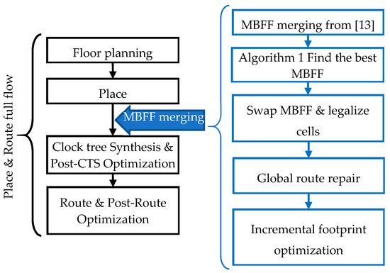
Figure 1.
Enhanced multi-bit flip-flop (MBFF) merging solution within the place and route flow.
Our previously presented methodology aimed to find the best location for the MBFF merging to maximize the MBFF utilization without degrading the circuit performance [13]. Here, our new solution focuses more on finding the best MBFF cell, which reduces the power consumption and maintains good timing. This new procedure searches among all the available, equivalent MBFF library (lib) cells and selects the best lib cell for reducing the power without generating any additional timing degradation. The following description provides more details regarding the proposed solution:
- Start with the MBFF merging solution from [13];
- Identify the best multi-bit flip-flop among all the available, equivalent MBFFs. The best MBFF is a flip-flop that has a smaller area and consumes less power without causing timing degradation. In order to do so, the following Algorithm 1 is used:
Algorithm 1. Find the best MBFF foreach cell in MBFF cell do get cell initial lib_cell “init_lib_cell” set best_lib_cell init_lib_cell get initial cell power “init_power” get initial max timing slack “init_max_slack.” get initial min timing slack “init_min_slack.” get initial max transition slack “init_transition_slack.” if init_max_slacks > 0 then foreach new_lib_cell in equivalent lib_cells Swap cell to new_lib_cell get new cell power “new_power” get new max timing slack “new_max_slack.” get new min timing slack “new_min_slack.” get new max transition slack “new_transition_slack.” if new_power < init_power AND new_max_slack ≥ 0 AND new_min_slack ≥ init_min_slack AND new_transition_slack ≥ init_transition_slack Then set best_lib_cell new_lib_cell set init_power new_power set init_max_slack new_max_slack set init_min_slack new_min_slack set init_transition_slack new_transition_slack END if END foreach Swap cell to best_lib_cell END if END foreach - Run global route with timing high effort for timing recovery on all nets;
- An incremental light timing optimization may be needed after having the accurate and updated net extraction;
- Report QoR (Timing, Power and Congestion).
Figure 2 shows a schematic view of an example case of the MBFF merging of eight single flip-flops into one MBFF with 8 bits. Figure 3 shows the corresponding layout view. The overall pin density is reduced significantly, because the scan enabler, clock pin, reset pin and scan input are shared in the MBFF implementation. Reducing the pin density reduces the short and design rule check (DRC) errors in the post-route stage. The total design area is also minimized, because the MBFF is optimized at the transistor level to fit multiple flip-flops and the overall area of an MBFF is always less than its equivalent single-bit flip-flops. However, the major benefit of the MBFF is the dynamic power reduction due mainly to the clock wirelength, the inputs’ pin capacitance and the clock buffers’ reduction. In the example shown in Figure 3, the clock net wirelength decreased from 28 µm to 11.04 µm.
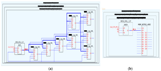
Figure 2.
Example of 8-bit MBFF merging (Schematic view): (a) Before the merge; (b) After the merge.
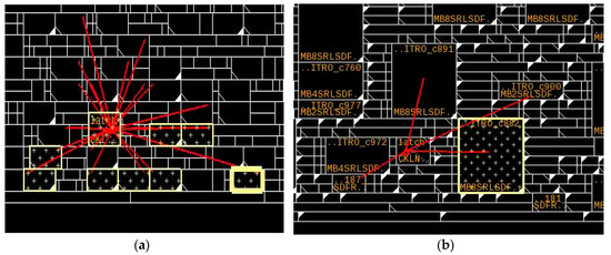
Figure 3.
Example of 8-bit MBFF merging (Layout View): (a) Before the merge; (b) After the merge.
3. Results and Analysis
3.1. New Solution’s Results Compared with the Prior Solution
In order to determine the best MBFF PnR procedure, the proposed solution (Figure 1) was integrated into the standard PnR process using the EDA tool, Nitro-SoC [16] and applied on a 7 nm design that functioned at a frequency of up to 2 GHz. Table 1 shows the main characteristics of the test case design used in this experiment and Figure 4 shows its floorplan.

Table 1.
Design characteristics.
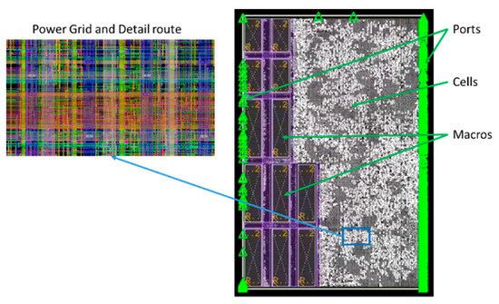
Figure 4.
Test case’s floorplan.
Table 2 highlights the improvements achieved by the new solution compared with the prior MBFF merging solution presented in Reference [13]. According to Table 2, the new approach results in an implementation process with an improved area and better utilization with no timing degradation. The greatest and most important improvement occurs in the congestion overflow, which produces an optimized routing topology and consequently reduces the overall power consumption. The “Overflow %” is a Nitro-SoC index that tell us the following: If the overflow is greater than 0.002%, then the design may be difficult to route. Thus, an overflow of 0.00007% indicates that our enhanced flow contributes to a more routable design.
Table 2.
Quality of Results (QoR) Summary. WNS: worst negative slack; TNS: total negative slack; and STD: standard.
3.2. Impact on Performance, Power Consumption and Area in the Full Physical Implementation Process
After ensuring good design performance at the placement stage, the impact of the inserted MBFFs on the power consumption was measured after the CTS phase. As expected, reductions of the clock wirelength, number of clock nets and number of clock buffer/inverter tree elements by 11.98%, 3.82% and 9.16%, respectively, were detected (Table 3). All these improved metrics help to reduce the power consumed by the registers, clock tree cells and nets. Throughout all steps, the total power gain remained well maintained.
Table 3.
Improvement in the clock tree wirelength, number of nets and number of tree elements.
The next step in this study was to complete the full PnR flow, including a complete clock tree synthesis followed by a complete nets routing and post-route optimization.
Table 4 presents the total power consumption and its improvement in the full flow context with and without the MBFF merging. The achieved area and wirelength reductions translated into a total power reduction of 2.67%, which mainly came from the clock components’ power reduction (20.84% in the registers, 22.11% in the clock nets and 12.38% in the clock cells).
Table 4.
Power results during the place and route steps.
The circuit’s physical area was tracked during this experiment by measuring the total numbers of buffers and inverters, the STD cell utilization and the total STD cell area at each step. In summary, a small area reduction of 1% was detected, which was acceptable and assured no area degradation. Table 5 presents the area improvement achieved in each step.
Table 5.
Impact on the area occupied by the standard cells.
The performance of the system with MBFF merging was well preserved at the end of the implementation flow, with a worst negative slack (WNS) of −3.4 ps compared with that of −7.8 ps for the baseline. Table 6 shows the timing results for the MBFF merging solution compared with those of the baseline. The hold timing stayed under an acceptable range.
Table 6.
Timing results of the MBFF solution compared with those of the baseline at the end of the implementation process. WHS: worst hold slack; THS: total hold slack.
Figure 5 illustrates the change in the power distribution in the design with and without MBFF merging. The total power distribution among all the power components is shown, including the Data Cells, Clock Cells, Combinational Cells, Macros Cells, Registers Cells, Clock Nets and Data Nets. The reduced percentage in the clock network evidences a total power consumption reduction from 14.2% to 11.55% in the registers cells, from 0.54% to 0.48% in the clock cells and from 1.29% to 1.03 in the clock nets.
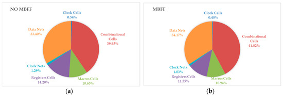
Figure 5.
Total power distribution at the end of the Post-Route optimization: (a) With No MBFF; (b) With MBFF merging.
4. Conclusions
Advanced technology nodes bring several performance improvements to modern integrated circuits. These challenges should be resolved to enable the full capacity of each technology to meet the market requirements and the users’ expectations. One major challenge is the trend of high power consumption, which is alarming the whole IC market and should be reduced considerably to meet reliability expectations and cost concerns without performance regression. To face these obstacles, researchers and developers at each level are required to develop new, innovative techniques for power optimization. This paper proposed an enhancement of a previously presented solution [13] to achieve better power reduction while maintaining good routability and the desired circuit performance. By using the new proposed solution, which can achieve a total MBFF merging of 76%, considerable improvements were realized in many different design metrics: a 11.98% reduction in the clock wirelength, a 3.82% reduction in the number of clock nets, a 9.16% reduction in the number of clock buffer/inverter tree elements and a small area reduction of 1%. All of these improvements led to a reduction in the total consumed power of 2.67%.
Author Contributions
L.C. conceived of and designed the experiments; L.C. performed the experiments with support from M.C and J.B.; L.C., M.C. and J.B. analysed the data; J.B. and M.D. contributed reagents/materials/analysis tools; and L.C, J.B., M.C. and M.D. wrote the paper. R.E. and N.H. supervised the project.
Funding
This research received no external funding.
Acknowledgments
We thank Hazem El-Tahawy (Mentor Graphics, Managing Director MENA Region) for initiating and supporting this work.
Conflicts of Interest
The authors declare no conflicts of interest.
References
- Radack, D.J.; Zolper, J.C. A Future of Integrated Electronics: Moving Off the Roadmap. Proc. IEEE 2008, 96, 198–200. [Google Scholar] [CrossRef]
- Lee, I.; Lee, K. The Internet of Things (IoT): Applications, investments and challenges for enterprises. Bus. Horiz. 2015, 58, 431–440. [Google Scholar] [CrossRef]
- Flynn, D.; Aitken, R.; Gibbons, A.; Shi, K. Low Power Methodology Manual: For System-On-Chip Design, 2nd ed.; Springer: Berlin/Heidelberg, Germany, 2007; p. 13. [Google Scholar]
- Rahman, M.; Afonso, R.; Tennakoon, H.; Sechen, C. Design automation tools and libraries for low power digital design. In Proceedings of the 2010 IEEE Dallas Circuits and Systems Workshop, Richardson, TX, USA, 17–18 October 2010. [Google Scholar]
- Lin, G.J.Y.; Hsu, C.B.; Kuo, J.B. Critical-path aware power consumption optimization methodology (CAPCOM) using mixed-VTH cells for low-power SOC designs. In Proceedings of the 2014 IEEE International Symposium on Circuits and Systems (ISCAS), Melbourne, VIC, Australia, 1–5 June 2014; pp. 1740–1743. [Google Scholar]
- Gautam, S. Analysis of multi-bit flip flop low power methodology to reduce area and power in physical synthesis and clock tree synthesis in 90nm CMOS technology. In Proceedings of the 2014 International Conference on Advances in Computing, Communications and Informatics (ICACCI), Greater Noida, New Delhi, 24–27 September 2014; pp. 570–574. [Google Scholar]
- Lin, M.P.H.; Hsu, C.C.; Chen, Y.C. Clock-Tree Aware Multibit Flip-Flop Generation During Placement for Power Optimization. IEEE Trans. Comput.-Aided Des. Integr. Circuits Syst. 2015, 34, 280–292. [Google Scholar] [CrossRef]
- Prakash, G.; Sathishkumar, K.; Sakthibharathi, B.; Saravanan, S.; Vijaysai, R. Achieving reduced area by Multi-bit Flip flop design. In Proceedings of the 2013 International Conference on Computer Communication and Informatics, Coimbatore, India, 4–6 January 2013; pp. 1–4. [Google Scholar]
- Lin, M.P.; Hsu, C.; Chang, Y. Post-Placement Power Optimization With Multi-Bit Flip-Flops. IEEE Trans. Comput.-Aided Des. Integr. Circuits Syst. 2011, 30, 1870–1882. [Google Scholar] [CrossRef]
- Hou, W.; Liu, D.; Ho, P.-H. Automatic register banking for low-power clock trees. In Proceedings of the 2009 10th International Symposium on Quality Electronic Design, San Jose, CA, USA, 16–18 March 2009; pp. 647–652. [Google Scholar]
- Feng, C.; Yue, D.; Zhao, Z.; Liao, Z. A parameterized timing-aware flip-flop merging algorithm for clock power reduction. In Proceedings of the 2018 Design, Automation & Test in Europe Conference & Exhibition (DATE), Dresden, Germany, 19–23 March 2018. [Google Scholar]
- Seitanidis, I.; Dimitrakopoulos, G.; Matheakis, P.; Masse-Navete, L.; Chinnery, D. Timing Driven Incremental Multi-Bit Register Composition Using a Placement-Aware ILP formulation. In Proceedings of the 54th Annual Design Automation Conference 2017, Austin, TX, USA, 18–22 June 2017. [Google Scholar]
- Cherif, L.; Chentouf, M.; Benallal, J.; Darmi, M.; Elgouri, R.; Hmina, N. Usage and impact of multi-bit flip-flops low power methodology on physical implementation. In Proceedings of the 2018 4th International Conference on Optimization and Applications (ICOA), Mohammedia, Morocco, 26–27 April 2018; pp. 1–5. [Google Scholar]
- Nitro-SoC™ and Olympus-SoC™ User’s Manual; Software Version 2017; Mentor Graphics Corporation: Wilsonville, OR, USA, August 2017.
- Nitro-SoC™ and Olympus-SoC™ Advanced Design Flows Guide; Software Version 2017; Mentor Graphics Corporation: Wilsonville, OR, USA, August 2017.
- Nitro-SoC™ and Olympus-SoC™; Software Version 2017.1.R2; Mentor Graphics Corporation: Wilsonville, OR, USA, August 2017.
© 2019 by the authors. Licensee MDPI, Basel, Switzerland. This article is an open access article distributed under the terms and conditions of the Creative Commons Attribution (CC BY) license (http://creativecommons.org/licenses/by/4.0/).