Tolerating Permanent Faults in the Input Port of the Network on Chip Router

Abstract
1. Introduction
2. Related Works
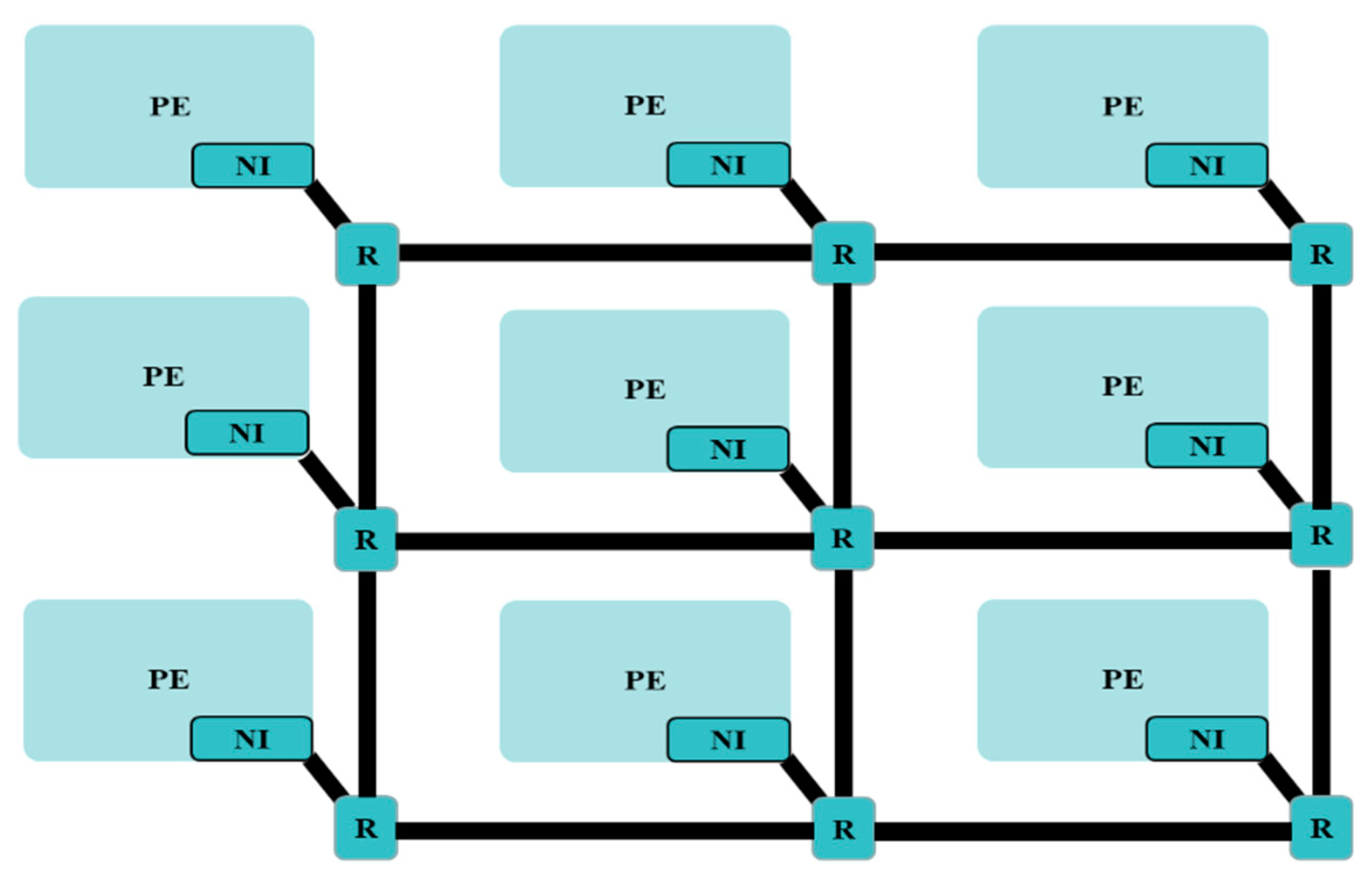
3. Baseline 4-Stage NoC Router
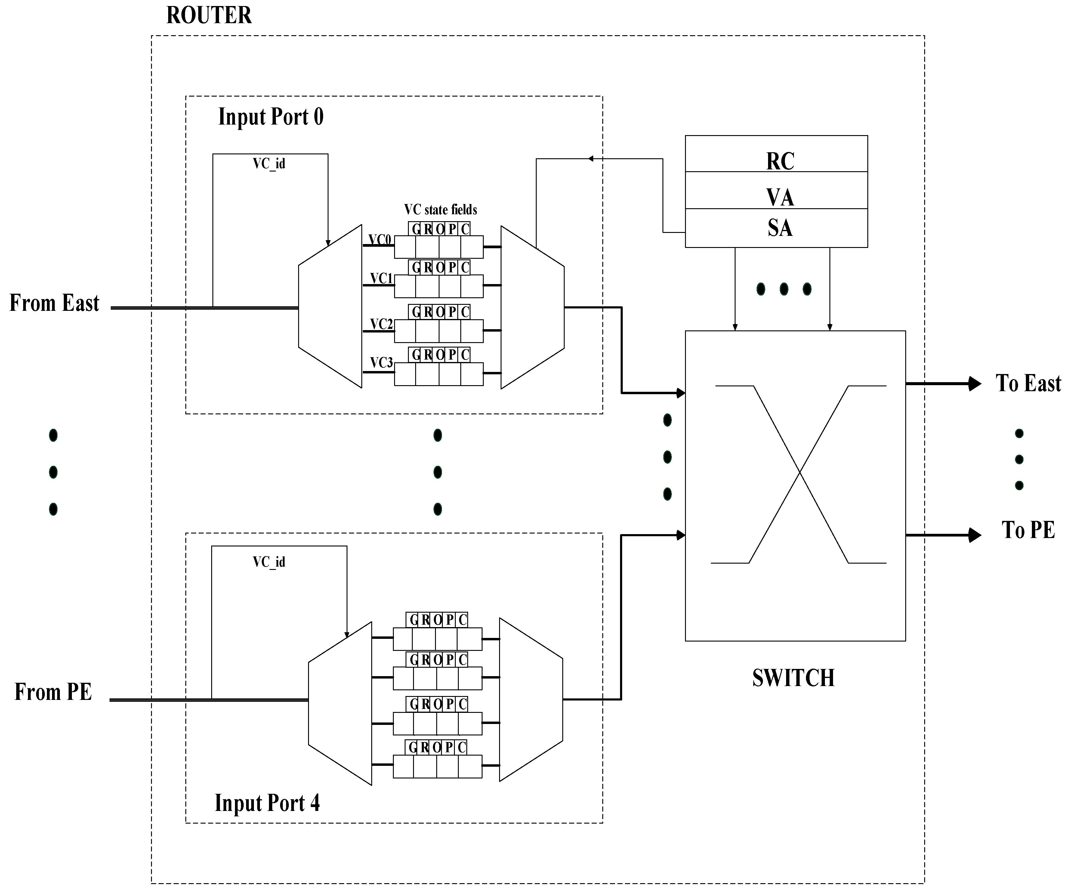
3.1. Router Architecture
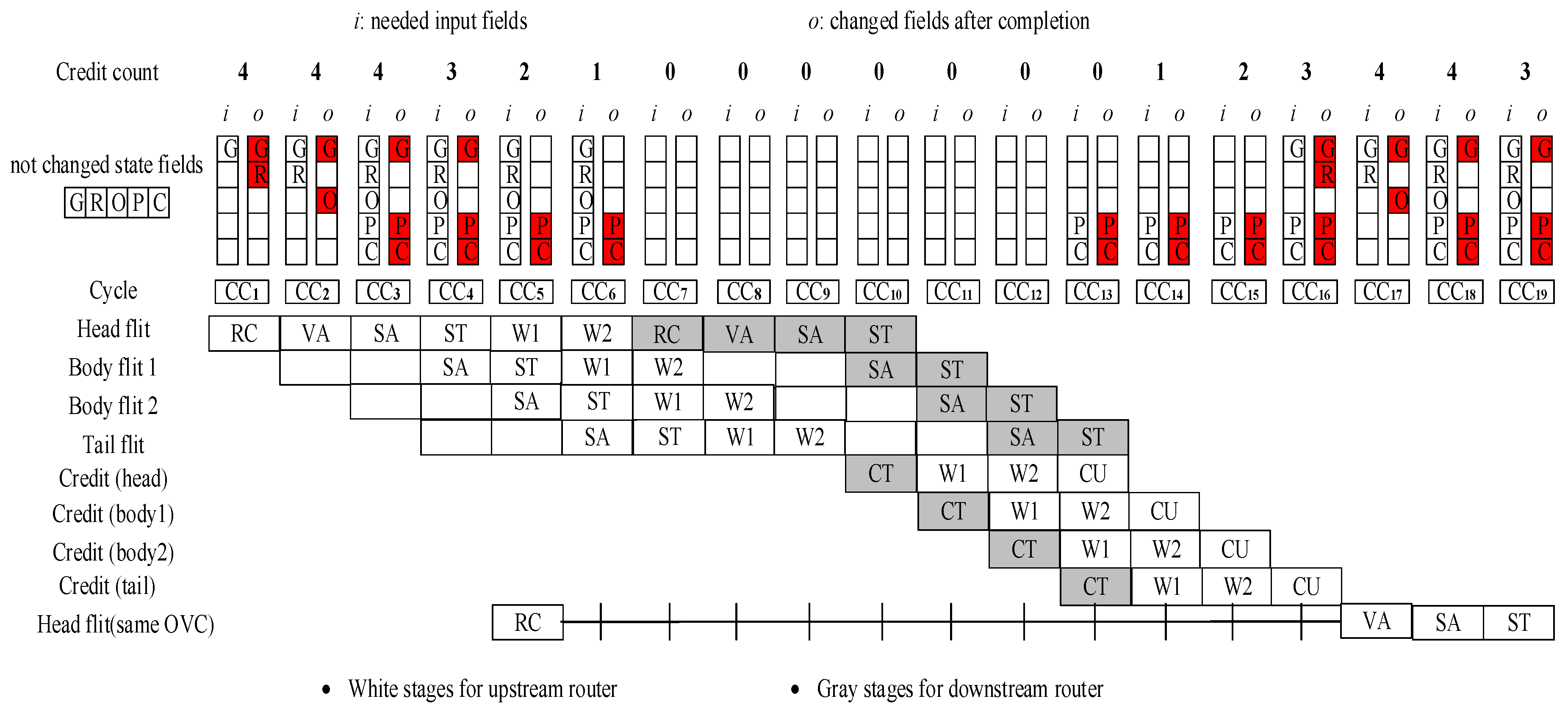
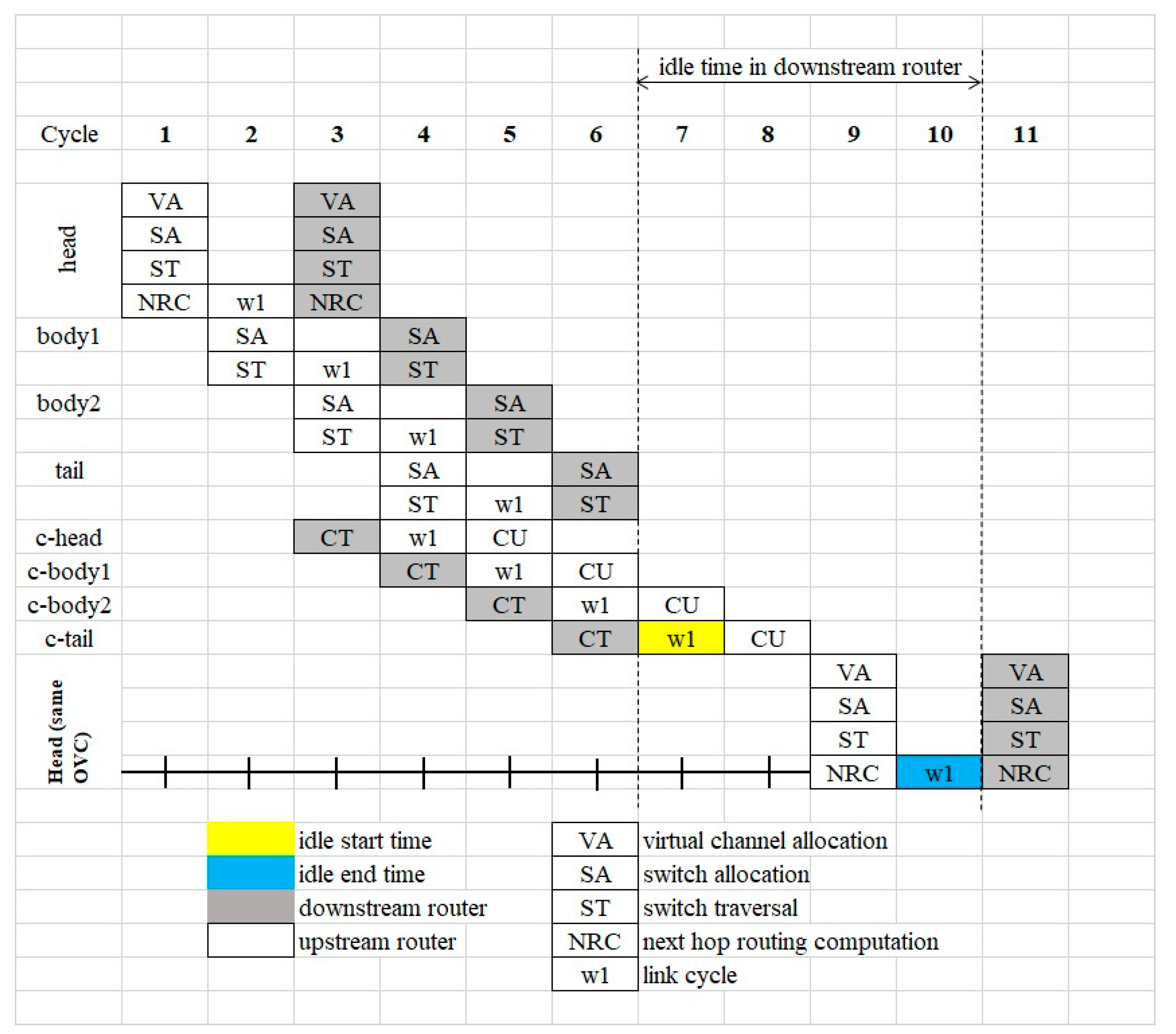
3.2. Router Pipeline
3.3. Architecture of Router Components
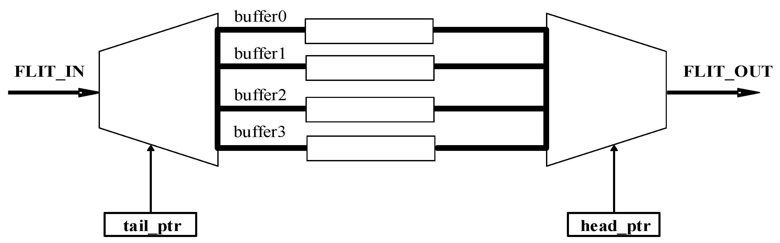
3.3.1. Input Buffer Component (Input Port Component)
3.3.2. Routing Computation Logic Component (RC)
3.3.3. Virtual Channel Allocation Component (VA)
3.3.4. Switch Allocation Component (SA)
3.3.5. Switch Traversal Component (Crossbar XB) or (ST)
3.4. Alternative Router Pipelines
4. Proposed NoC Router
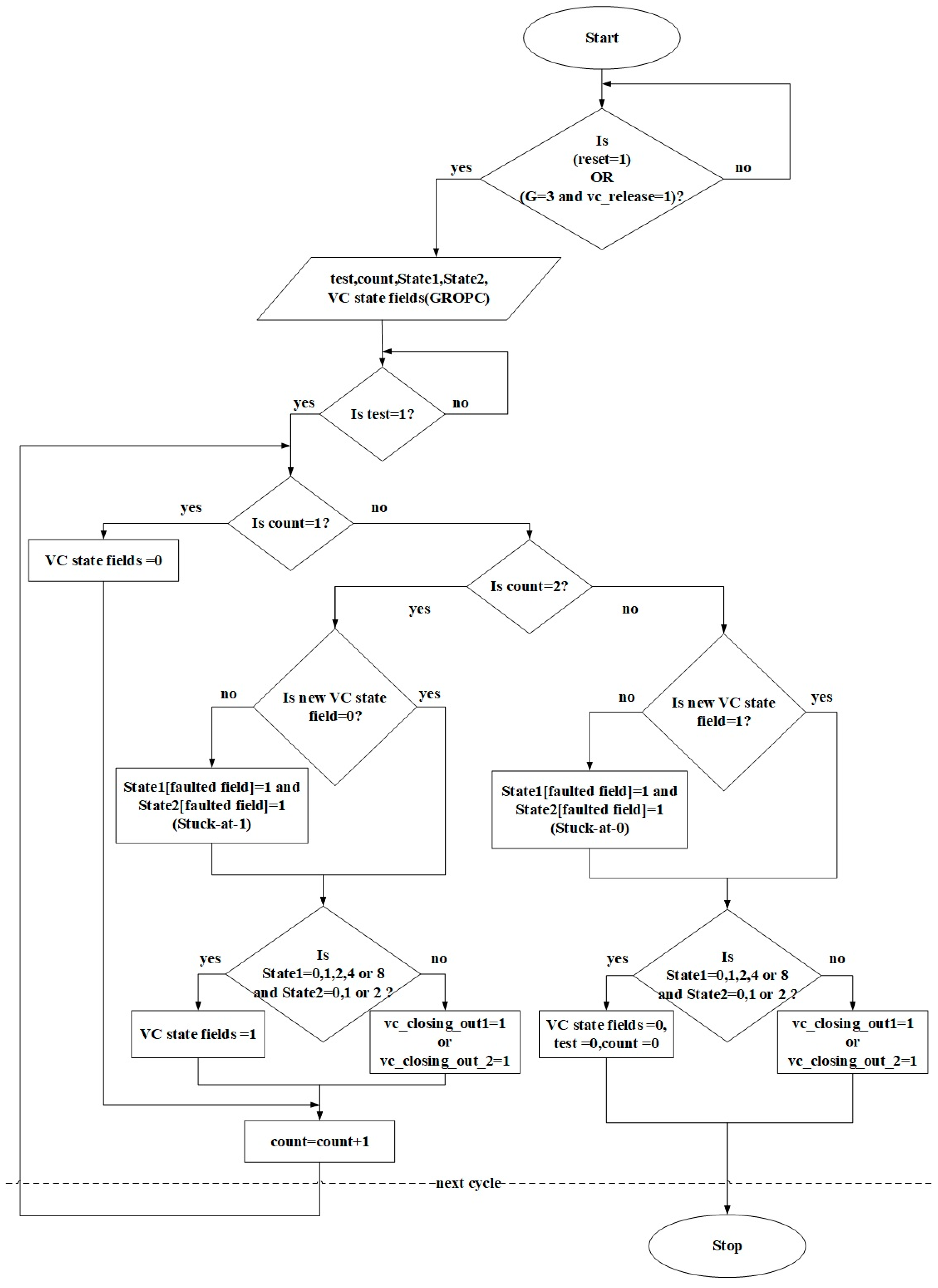
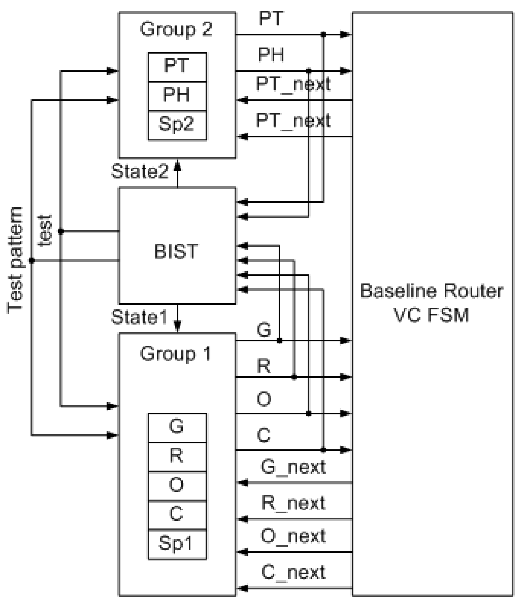
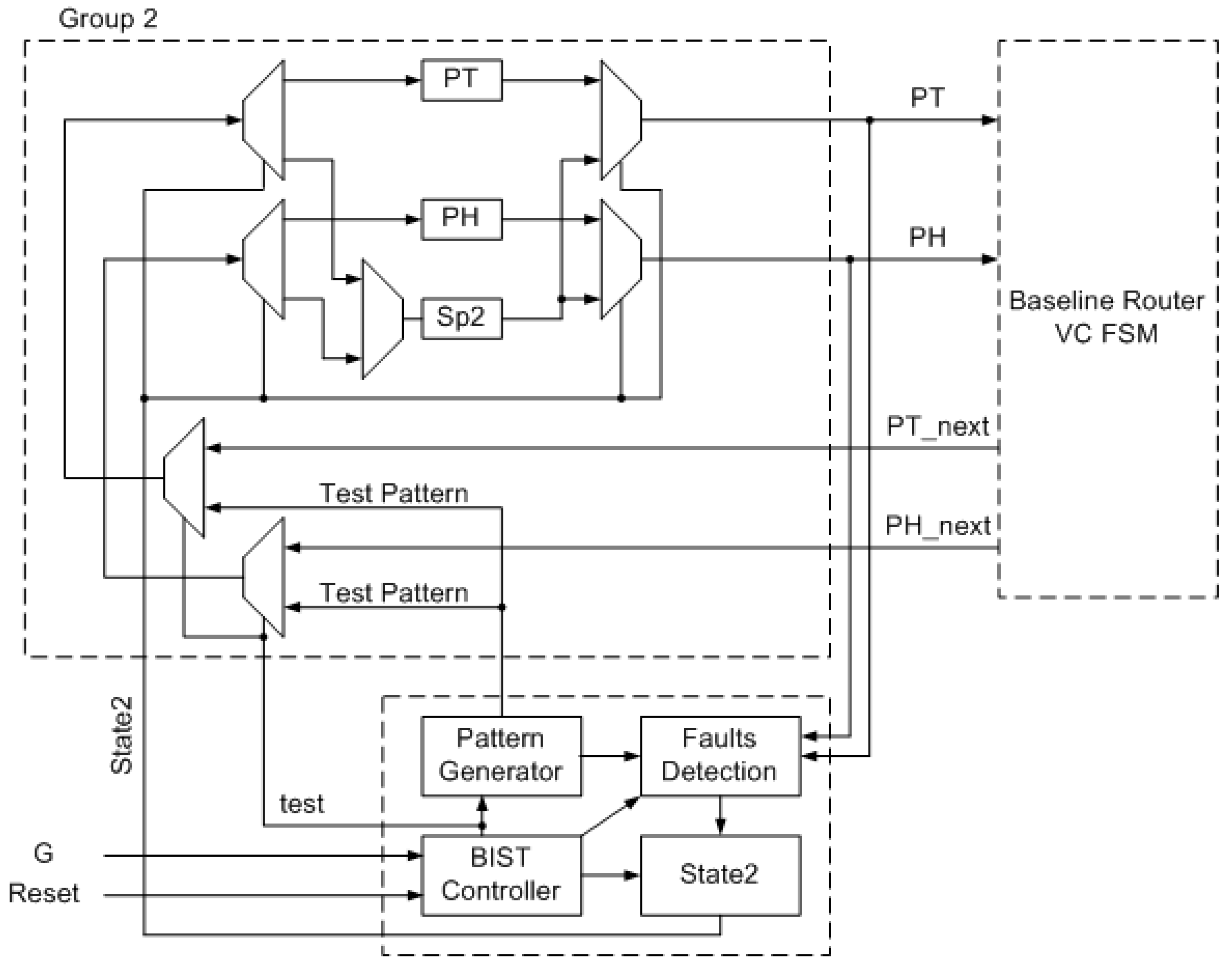
4.1. Detection Mechanism
4.2. Hardware Redundancy Technique
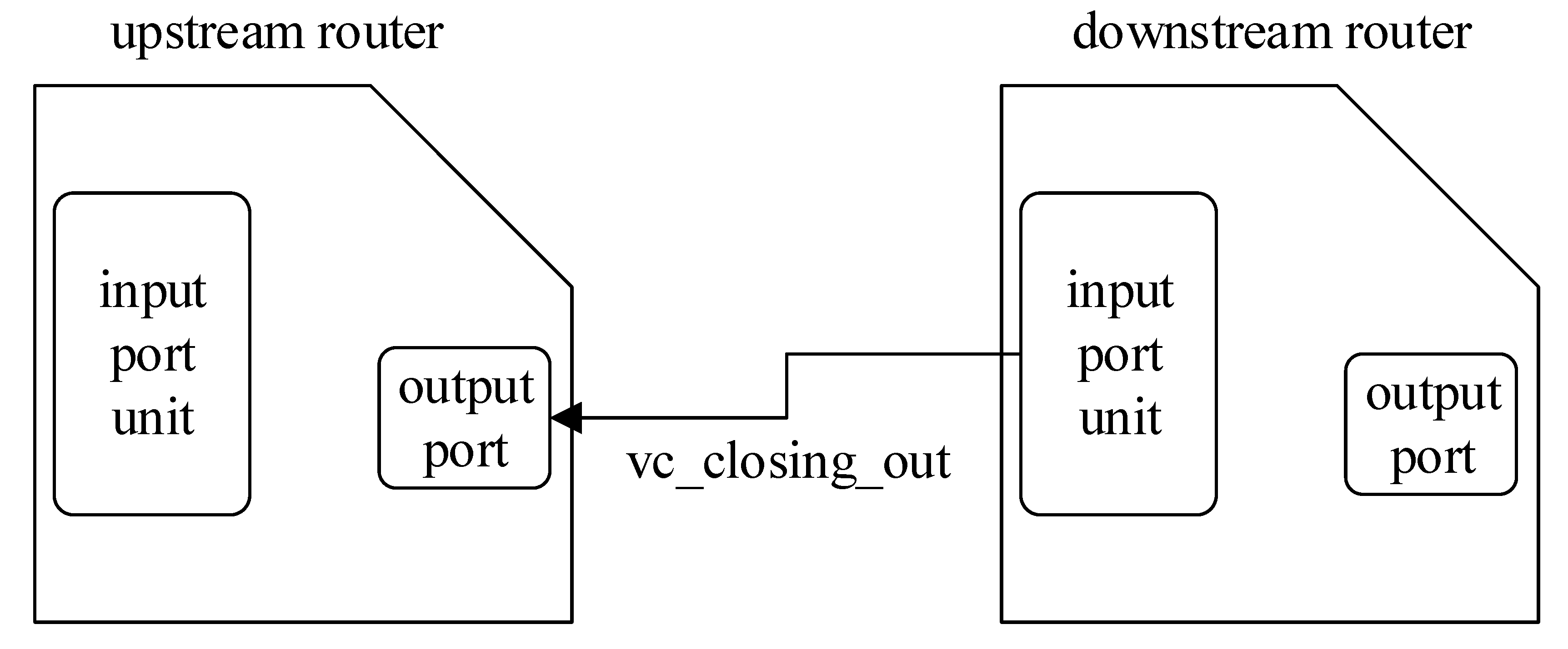
4.3. VC-Closing Property
5. Results and Discussion
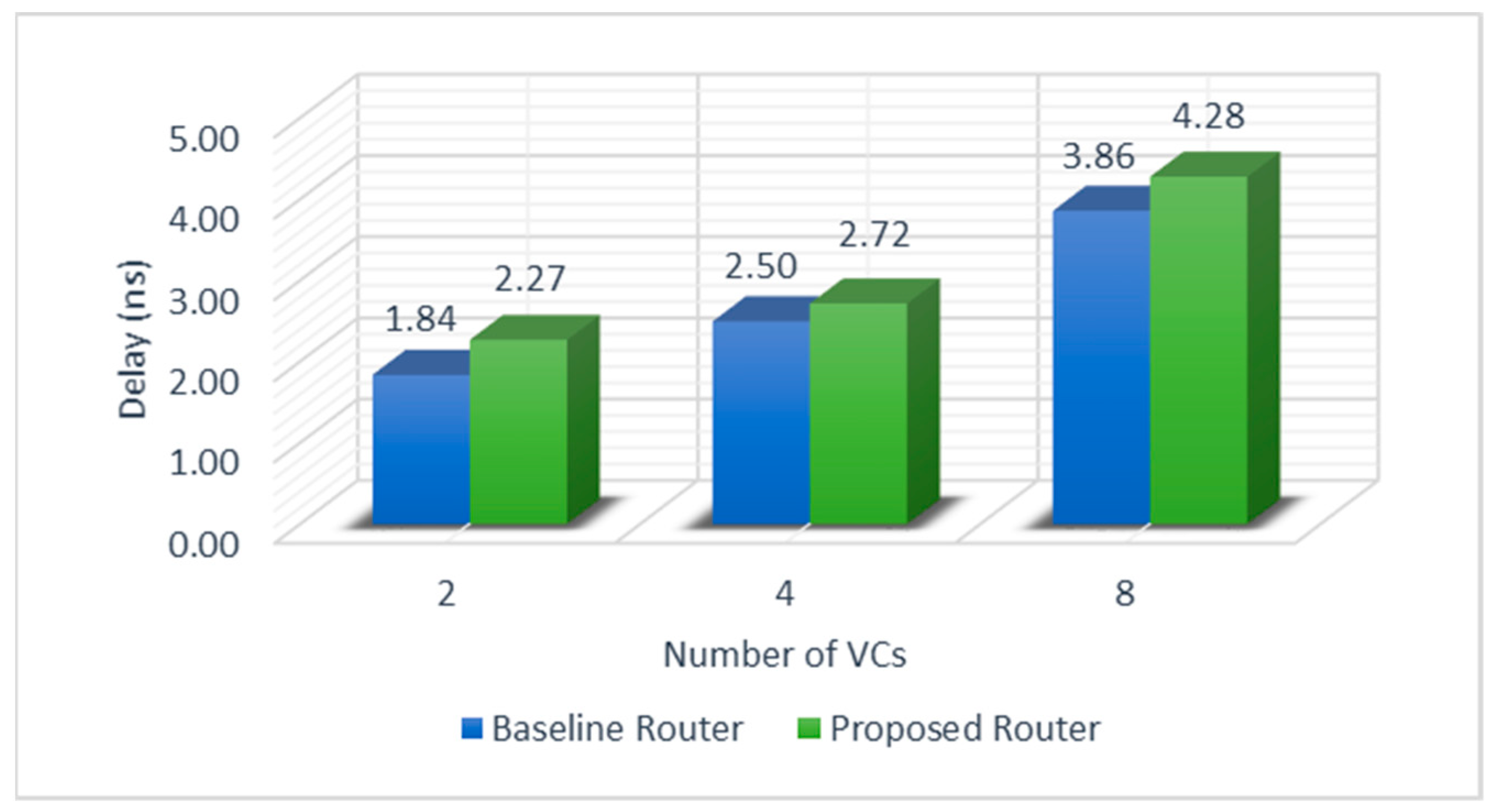
5.1. Critical Path Delay Analysis
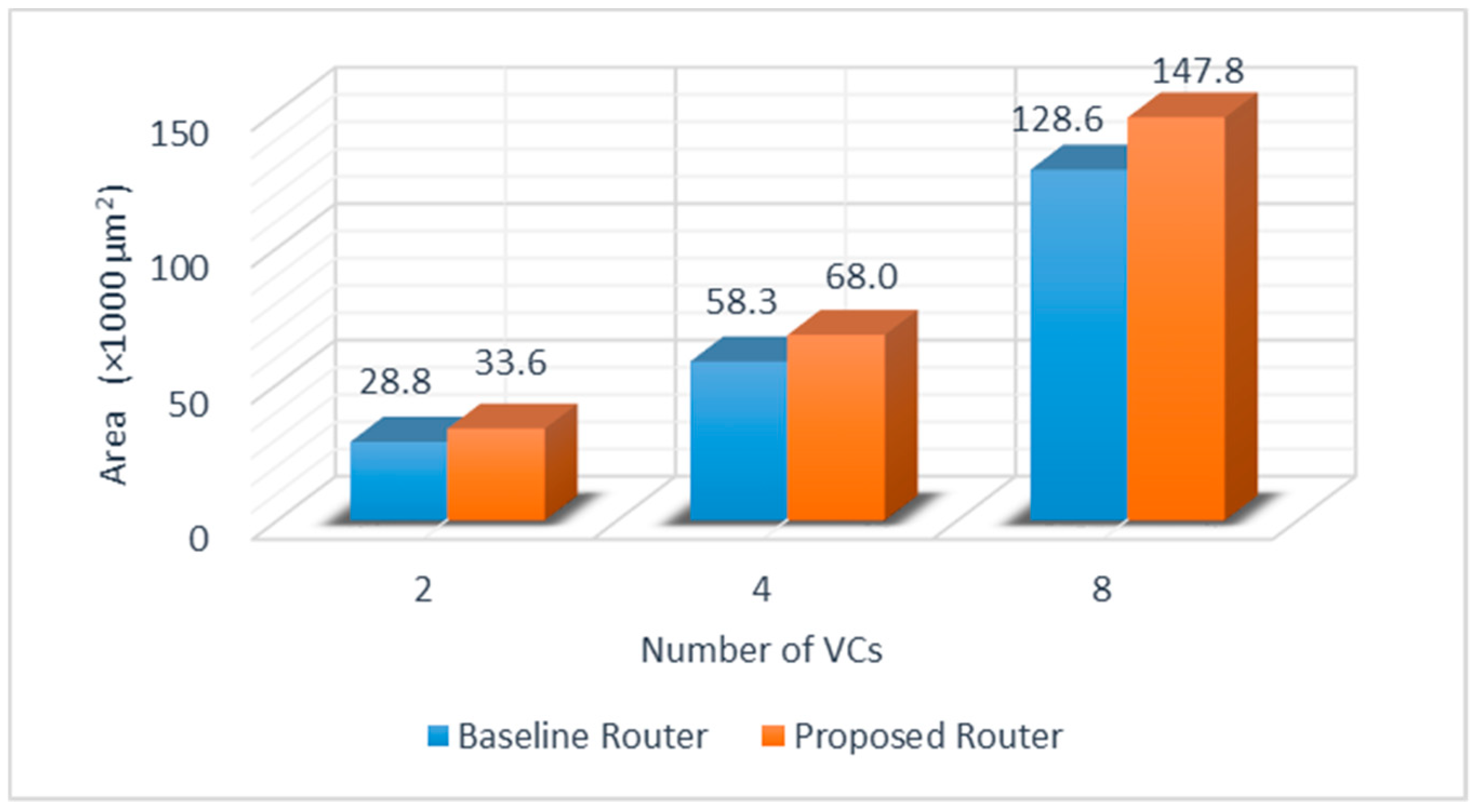
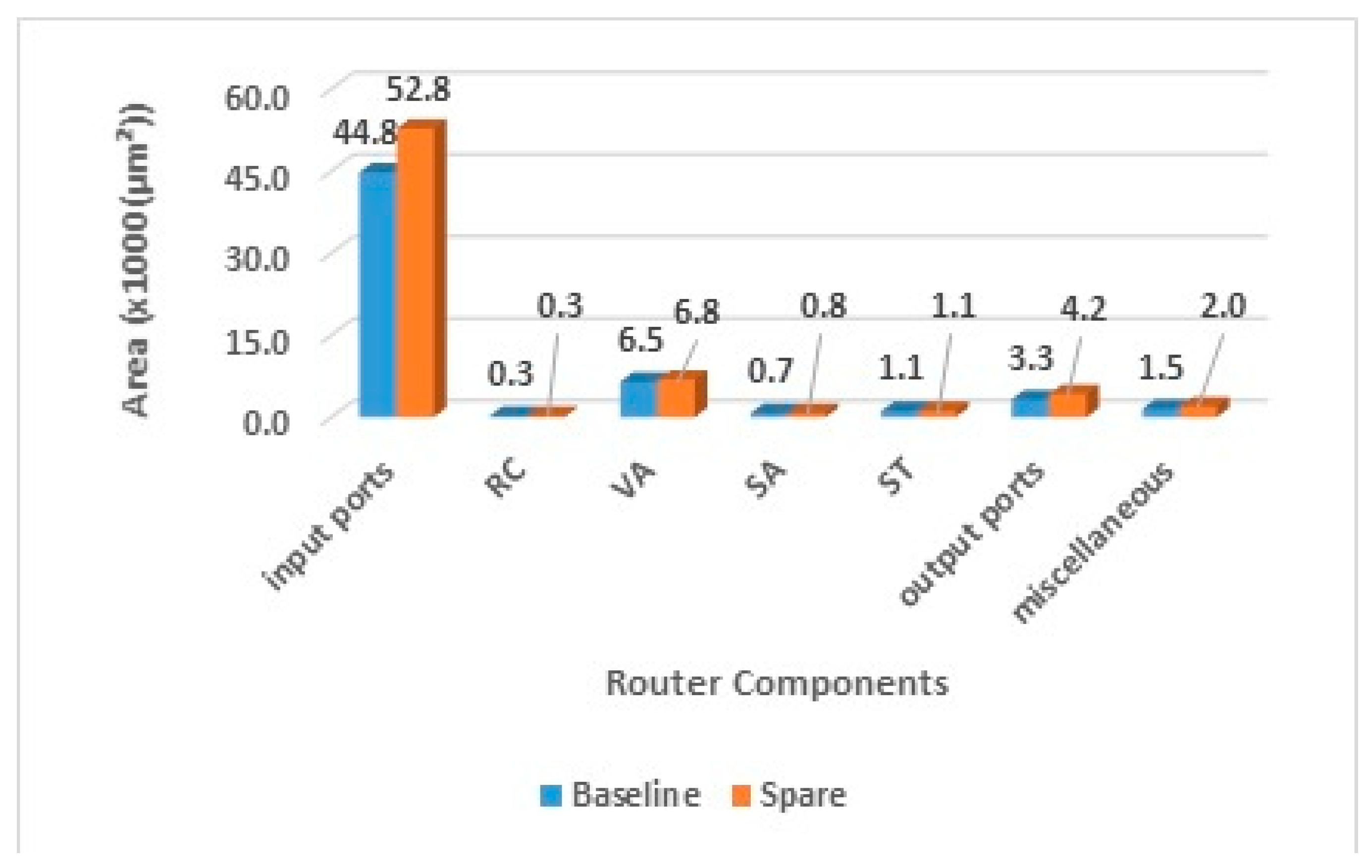
5.2. Area Analysis
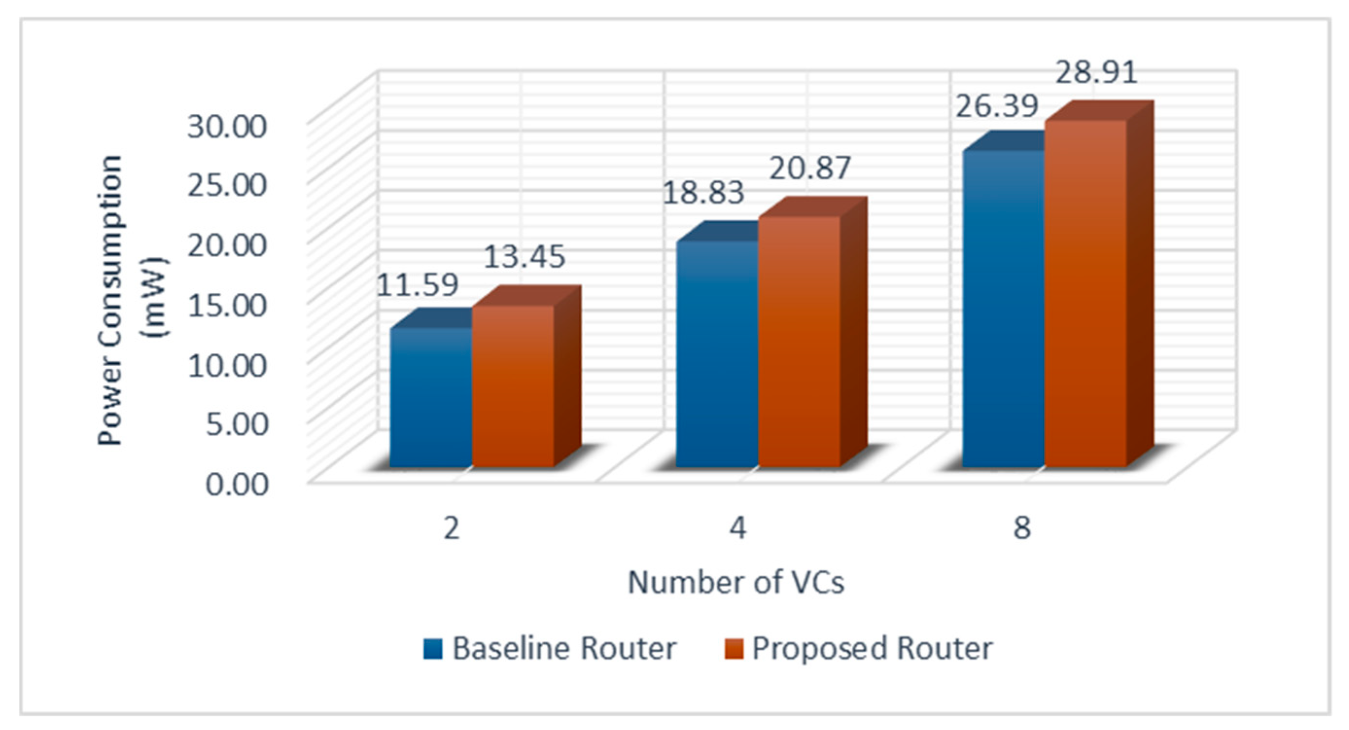
5.3. Power Analysis
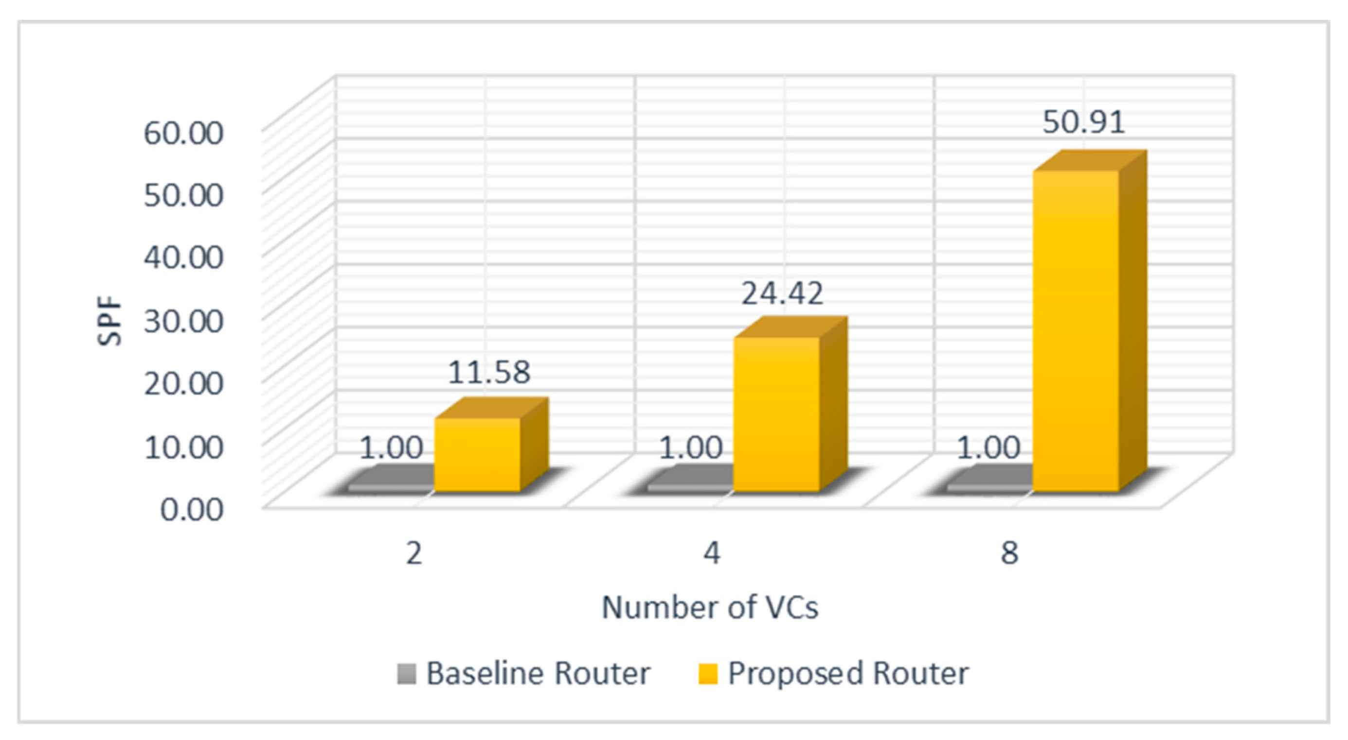
5.4. Reliability Improvement
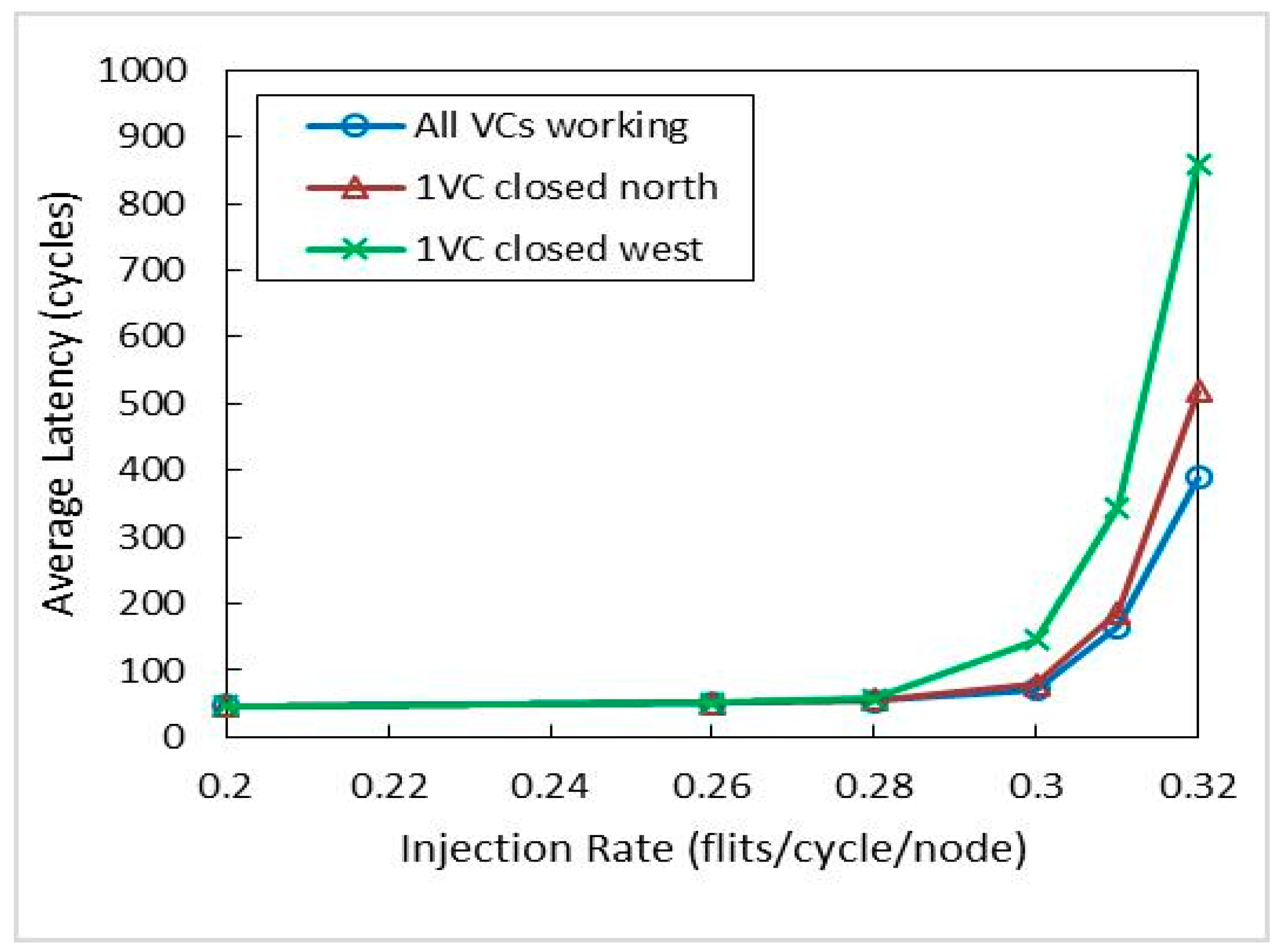
5.5. Latency Analysis
6. Conclusions
Author Contributions
Funding
Acknowledgments
Conflicts of Interest
References
- Singh, S.K.; Mondal, A.J.; Majumder, A. Generation and Performance Evaluation of Reconfigurable Fault Tolerant Routing Algorithm for 2D-Mesh NoC. Procedia Comput. Sci. 2015, 57, 232–240. [Google Scholar] [CrossRef]
- Xu, J.; Wolf, W.; Henkel, J.; Chakradhar, S. A methodology for design, modeling, and analysis of networks-on-chip. In Proceedings of the IEEE International Symposium on Circuits and Systems, Kobe, Japan, 23–26 May 2005; pp. 1778–1781. [Google Scholar]
- Kamali, H.M.; Azar, K.Z.; Hessabi, S. DuCNoC: A High-Throughput FPGA-Based NoC Simulator using Dual-Clock Lightweight Router Micro-Architecture. IEEE Trans. Comput. 2018, 67, 208–221. [Google Scholar] [CrossRef]
- Todman, T.J.; Constantinides, G.A.; Wilton, S.J.E.; Mencer, O.; Luk, W.; Cheung, P.Y.K. Reconfigurable computing: Architectures and design methods. IEE Proc.-Comput. Digit. Tech. 2005, 152, 193–207. [Google Scholar] [CrossRef]
- Wang, C.; Hu, W.-H.; Bagherzadeh, N. Scalable load balancing congestion-aware Network-on-Chip router architecture. J. Comput. Syst. Sci. 2013, 79, 421–439. [Google Scholar] [CrossRef]
- Benini, L.; De Micheli, G. Networks on chips: A new SoC paradigm. Computer 2002, 35, 70–78. [Google Scholar] [CrossRef]
- Bjerregaard, T.; Mahadevan, S. A survey of research and practices of Network-on-chip. ACM Comput. Surv. 2006, 38, 1. [Google Scholar] [CrossRef]
- Vangal, S.; Howard, J.; Ruhl, G.; Dighe, S.; Wilson, H.; Tschanz, J.; Finan, D.; Iyer, P.; Singh, A.; Jacob, T.; et al. An 80-Tile 1.28TFLOPS Network-on-Chip in 65nm CMOS. In Proceedings of the 2007 IEEE International Solid-State Circuits Conference. Digest of Technical Papers, San Francisco, CA, USA, 11–15 February 2007; pp. 98–99. [Google Scholar]
- Dally, W.; Towles, B. Principles and Practices of Interconnection Networks; Morgan Kaufmann: Burlington, MA, USA, 2004. [Google Scholar]
- Dang, K.N.; Ben Ahmed, A.; Tran, X.-T.; Okuyama, Y.; Abdallah, A. Ben A comprehensive reliability assessment of fault-resilient network-on-chip using analytical model. IEEE Trans. Very Large Scale Integr. Syst. 2017, 25, 3099–3112. [Google Scholar] [CrossRef]
- Pande, P.P.; Grecu, C.; Ivanov, A.; Saleh, R.; De Micheli, G. Design, synthesis, and test of networks on chips. Des. Test Comput. IEEE 2005, 22, 404–413. [Google Scholar] [CrossRef]
- Sui, P.-H.; Wang, S.-D. An improved algorithm for fault-tolerant wormhole routing in meshes. IEEE Trans. Comput. 1997, 46, 1040–1042. [Google Scholar]
- Ziegler, J.F. Terrestrial cosmic rays. IBM J. Res. Dev. 1996, 40, 19–39. [Google Scholar] [CrossRef]
- Vrudhula, S.B.K.; Blaauw, D.; Sirichotiyakul, S. Estimation of the likelihood of capacitive coupling noise. In Proceedings of the 39th annual Design Automation Conference, New Orleans, LA, USA, 10–14 June 2002; pp. 653–658. [Google Scholar]
- Kuhn, K.J. Reducing variation in advanced logic technologies: Approaches to process and design for manufacturability of nanoscale CMOS. In Proceedings of the 2007 IEEE International Electron Devices Meeting, Washington, DC, USA, 10–12 December 2007; pp. 471–474. [Google Scholar]
- Hu, C.-K.; Rosenberg, R.; Rathore, H.S.; Nguyen, D.B.; Agarwala, B. Scaling effect on electromigration in on-chip Cu wiring. In Proceedings of the IEEE 1999 International Interconnect Technology Conference, San Francisco, CA, USA, 26 May 1999; pp. 267–269. [Google Scholar]
- Wu, E.; Sune, J.; Lai, W.; Nowak, E.; McKenna, J.; Vayshenker, A.; Harmon, D. Interplay of voltage and temperature acceleration of oxide breakdown for ultra-thin gate oxides. Solid. State. Electron. 2002, 46, 1787–1798. [Google Scholar] [CrossRef]
- Radetzki, M.; Feng, C.; Zhao, X.; Jantsch, A. Methods for fault tolerance in networks-on-chip. ACM Comput. Surv. 2013, 46, 1–38. [Google Scholar] [CrossRef]
- Constantinides, K.; Plaza, S.; Blome, J.; Zhang, B.; Bertacco, V.; Mahlke, S.; Austin, T.; Orshansky, M. BulletProof: A defect-tolerant CMP switch architecture. In Proceedings of the Twelfth International Symposium on High-Performance Computer Architecture, Austin, TX, USA, 11–15 February 2006; pp. 5–16. [Google Scholar]
- Fick, D.; DeOrio, A.; Hu, J.; Bertacco, V.; Blaauw, D.; Sylvester, D. Vicis: A reliable network for unreliable silicon. In Proceedings of the 46th Annual Design Automation Conference, San Francisco, CA, USA, 26–31 July 2009; pp. 812–817. [Google Scholar]
- Das, C.R.; Yousif, M.S.; Narayanan, V.; Park, D.; Nicopoulos, C.; Kim, J.; Das, C.R.; Yousif, M.S.; Narayanan, V.; Park, D.; et al. A Gracefully Degrading and Energy-Efficient Modular Router Architecture for On-Chip Networks. In Proceedings of the 33rd International Symposium on Computer Architecture (ISCA’06), Boston, MA, USA, 17–21 June 2006; pp. 4–15. [Google Scholar]
- Poluri, P.; Louri, A. An improved router design for reliable on-chip networks. In Proceedings of the 2014 IEEE 28th International Parallel and Distributed Processing Symposium, Phoenix, AZ, USA, 19–23 May 2014; pp. 283–292. [Google Scholar]
- Wang, L.; Ma, S.; Li, C.; Chen, W.; Wang, Z. A high performance reliable NoC router. Integr. VLSI J. 2017, 58, 583–592. [Google Scholar] [CrossRef]
- Poluri, P.; Louri, A. Shield: A reliable network-on-chip router architecture for chip multiprocessors. IEEE Trans. Parallel Distrib. Syst. 2016, 27, 3058–3070. [Google Scholar] [CrossRef]


| State Field | Function | Faults Effect |
|---|---|---|
| G (Global state) | Represents the status of the current virtual channel: idle (I), routing (R), waiting for an output VC (V), active (A), or waiting for credits (C). | The state of VC is changed. Many effects can occur but in general, the pipelined operation will not proceed correctly or may stop. |
| R (Route) | Stores the output port for the packet and is set after the routing computation stage is completed. | The packet is misrouted. |
| O (Output VC) | Holds the output VC of port R assigned to the current input VC which is the result of the virtual channel allocation stage. | The wrong O leads to wrong output VC. Packet(s) may be lost. |
| P (Pointers) | Stores the head flit and tail flit pointers that point to the buffers in the input VC. | The faulted P leads to pointing on the wrong location of buffers. Flits or even packet can be lost, and VC may stay unreleased. |
| C (Credit count) | Indicates the credits count of available downstream flit buffers for output virtual channel O on output port R. | If C is wrong, then the number of free buffers in output VC is wrong. Flits may be forwarded to a full buffer or flits may stay while the buffer is available. |
| Architecture | Area | #Mean Permanent Faults to Cause Failure | Fault Tolerance Methods | SPF |
|---|---|---|---|---|
| Poluri Router [24] | 31% | 15 | Redundant RC unit, sharing arbiters for VA, bypass path for arbiters of SA, and two paths for a crossbar. | 11 |
| Wang Router [23] | 30% | 28.5 | ECC detection and VC closing strategy for input buffer faults, double routing strategy for RC faults, default winner strategy for VA, runtime arbiter selection strategy for SA, and a crossbar with double bypass bus. | 21.9 |
| Proposed Router | 17% | 28.5 | BIST detection, VC-closing strategy, and Hardware Redundancy technique for input virtual channel state fields. | 24.35 |
| Fundamental Component (FC) | FIT of FC | #FCs | FIT of FCs |
|---|---|---|---|
| 32-bit DFF (BF) | 0.5 | 5 × 4 × 4 | 1280 |
| 11-bit input VC state fields DFF Group1 (G1) | 0.5 | 5 × 4 | 110 |
| 4-bit input VC state fields DFF Group2 (G2) | 0.5 | 5 × 4 | 40 |
| Fundamental Component (FC) | FIT of FC | #FCs | FIT of FCs |
|---|---|---|---|
| 3-bit DFF (Sp1) | 0.5 | 5 × 4 | 30 |
| 4-bit DFF (State 1) | 0.5 | 5 × 4 | 40 |
| Fundamental Component (FC) | FIT of FC | #FCs | FIT of FCs |
|---|---|---|---|
| 2-bit DFF (Sp2) | 0.5 | 5 × 4 | 20 |
| 2-bit DFF (State 2) | 0.5 | 5 × 4 | 20 |
© 2019 by the authors. Licensee MDPI, Basel, Switzerland. This article is an open access article distributed under the terms and conditions of the Creative Commons Attribution (CC BY) license (http://creativecommons.org/licenses/by/4.0/).
Share and Cite
Mohammed, H.J.; Flayyih, W.N.; Rokhani, F.Z. Tolerating Permanent Faults in the Input Port of the Network on Chip Router. J. Low Power Electron. Appl. 2019, 9, 11. https://doi.org/10.3390/jlpea9010011
Mohammed HJ, Flayyih WN, Rokhani FZ. Tolerating Permanent Faults in the Input Port of the Network on Chip Router. Journal of Low Power Electronics and Applications. 2019; 9(1):11. https://doi.org/10.3390/jlpea9010011
Chicago/Turabian StyleMohammed, Hala J., Wameedh N. Flayyih, and Fakhrul Z. Rokhani. 2019. "Tolerating Permanent Faults in the Input Port of the Network on Chip Router" Journal of Low Power Electronics and Applications 9, no. 1: 11. https://doi.org/10.3390/jlpea9010011
APA StyleMohammed, H. J., Flayyih, W. N., & Rokhani, F. Z. (2019). Tolerating Permanent Faults in the Input Port of the Network on Chip Router. Journal of Low Power Electronics and Applications, 9(1), 11. https://doi.org/10.3390/jlpea9010011