Review

A Recent Progress of Spintronics Devices for Integrated Circuit Applications

by
Tetsuo Endoh
1,2,3,4,*,† and
Hiroaki Honjo
1,†
1
Center for Innovative Integrated Electronic Systems, Tohoku University, Sendai 980-0845, Japan
2
Graduate School of Engineering, Tohoku University, Sendai 980-8579, Japan
3
Center for Spintronics Research Network, Tohoku University, Sendai 980-8577, Japan
4
Center for Science and Innovation in Spintronics (Core Research Cluster), Tohoku University, Sendai 980-8577, Japan
*
Author to whom correspondence should be addressed.
JST-ACCEL, Saitama 332-0012, Japan.
J. Low Power Electron. Appl. 2018, 8(4), 44; https://doi.org/10.3390/jlpea8040044
Submission received: 28 October 2018 / Revised: 9 November 2018 / Accepted: 9 November 2018 / Published: 13 November 2018
(This article belongs to the Special Issue Spin-Orbit Torque/Voltage-Controlled MRAM and Low Power Application)

Abstract

:
Nonvolatile (NV) memory is a key element for future high-performance and low-power microelectronics. Among the proposed NV memories, spintronics-based ones are particularly attractive for applications, owing to their low-voltage and high-speed operation capability in addition to their high-endurance feature. There are three types of spintronics devices with different writing schemes: spin-transfer torque (STT), spin-orbit torque (SOT), and electric field (E-field) effect on magnetic anisotropy. The NV memories using STT have been studied and developed most actively and are about to enter into the market by major semiconductor foundry companies. On the other hand, a development of the NV memories using other writing schemes are now underway. In this review article, first, the recent advancement of the spintronics device using STT and the NV memories using them are reviewed. Next, spintronics devices using the other two writing schemes (SOT and E-field) are briefly reviewed, including issues to be addressed for the NV memories application.

1. Introduction

Large-scale integrated (LSI) circuits are a vital constituent for current information and communication technology equipment. Progress in the LSIs have been led by development of complementary metal-oxide-semiconductor (CMOS) technology relying on Moore’s scaling law. However, the development of CMOS is now interrupted mainly by two serious issues. One is an increase of standby power and the other is Input/Output (I/O) bottleneck due to interconnection delay. The former issue originates from the volatile nature of the current memories in the LSIs in which the standby power becomes larger due to an increase of leakage current as the CMOS technology node is advancing. The latter issue is attributed to an elongation of global wire length due to an increase of the number of integrated elements in the LSIs. To address those issues, nonvolatile (NV) memories have been attracting a great deal of attention. Among the proposed NV memories, spintronics-based ones (magnetoresistive random access memories (MRAM)) are very attractive owing to their high-speed and low-voltage operation capability and high endurance, which are required for working memory usage [1,2,3]. In addition to those advantages, spintronics-based memories can be implemented in back-end-of-line (BEOL), a feature which enables one to address the I/O bottleneck as global wire length between memory and logic module can be reduced.
The proposed three writing schemes are spin-transfer torque (STT), spin-orbit torque (SOT), and electric field (E-field) effect on magnetic anisotropy or voltage-controlled (VC) magnetic anisotropy. The memory cell for STT-MRAM and VC-MRAM is a two-terminal structure and that for SOT-MRAM is a three-terminal structure as shown in Figure 1a,b, respectively. In the STT-MRAM, the memory cell with minimum cell size is composed of one magnetic tunnel junction (MTJ) and one selective MOS transistor (1T-1MTJ) as shown in Figure 1a. Note that there are many variations of the memory cell depending on applications. For writing, the current is applied to the MTJ from the transistor, which exerts a spin-transfer torque on the magnetization in the free layer of the MTJ [4,5]. In SOT-MRAM, a current is applied to the channel layer from the transistor located at the side of the channel layer underneath the MTJ and a torque is exerted on the magnetization in the free layer of the MTJ through spin Hall effect and/or Rashba–Edelstine effect [6,7,8]. For VC-MRAM, E-field (voltage) is applied to the free layer in the MTJ, which reduces or increases perpendicular magnetic anisotropy. The easy axis of magnetization transits from out-of-plane to in-plane or vice versa at a certain E-field. Above the E-field, the magnetization can be switched through precessional motion of magnetization along in-plane (out-of-plane) magnetic field.
There are three types of MRAM where different writing schemes are employed. In all the MRAMs, a magnetic tunnel junction is integrated as storage element. For reading operation, tunnel magnetoresistance effect is utilized, by which two distinct resistance levels can be obtained depending on magnetization configuration for free and reference layers, parallel and antiparallel states.
The STT-MRAM is the most studied and developed MRAM and is about to enter the market as major semiconductor foundries have announced the starting of risk of mass production in 2018. Although the STT-MRAM is about to enter the market, the other MRAMs have been also intensively studied [9]. This is because those two MRAMs, in principle, have higher potential in offering high-speed writing operation compared with the STT-MRAM.
In this review, first, we show benchmarking results for the STT-MRAM, SOT-MRAM, and E-field MRAM from the viewpoint of LSI applications (Section 2). In Section 3, we review the recent progress of STT-MRAMs mainly based on our efforts (Section 3.1) and briefly review the progress of SOT-MRAM and E-field MRAM including the issues to be addressed for NV memory applications (Section 3.2 and Section 3.3).

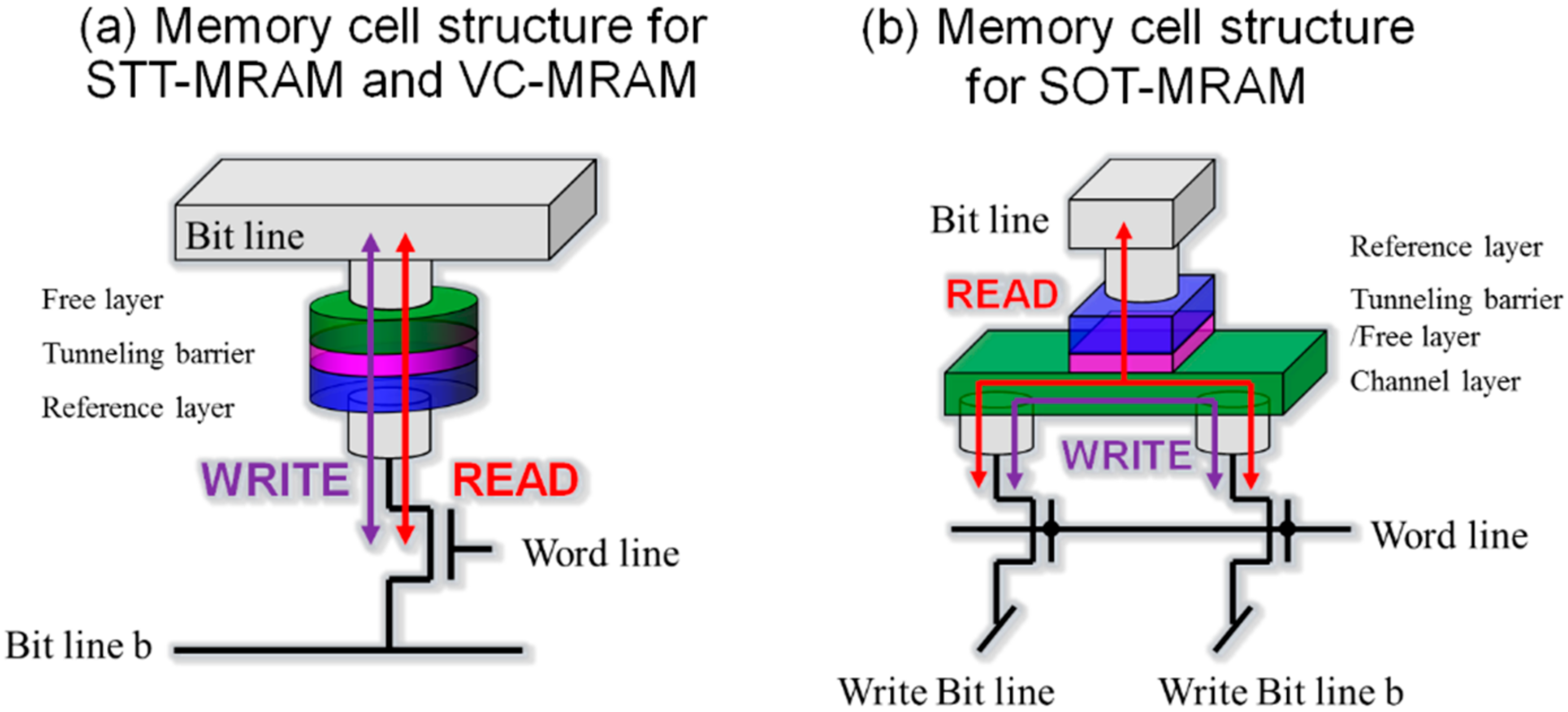
2. Benchmarking Results for STT-MRAM, SOT-MRAM, and E-Field MRAM

In this section, we show benchmarking results for the STT-MRAM, SOT-MRAM, and E-field MRAM compared with eFlash and SRAM as CMOS-based memories. Table 1 shows the benchmarking results [2,10,11,12,13]. Thanks to the simple memory cell structure for the STT-MRAM, the STT-MRAM has been developed for replacement of SRAM and eFlash. For SRAM replacement usage, the STT-MRAM enables one to reduce cell size and nonvolatility function, resulting in drastic reduction of standby power, without significant degradation of high-speed operation capability and endurance. For eFlash replacement, the STT-MRAM gives us lower write voltage, faster write speed, and better endurance without sacrificing nonvolatility.
SOT-MRAM and VC-MRAM are very attractive for SRAM replacement usage as, in principle, they have higher potential in offering high-speed writing capability than the STT-MRAM. However, there are a few issues in SOT-MRAM and VC-MRAM to be addressed for NV memory applications, which will be discussed later.

3. Review for Recent Progress of STT-MRAM, SOT-MRAM, and E-Field MRAM

3.1. Recent Progress of STT-MRAMs for NV Memory Applications

STT-MRAMs are attracting much attention owing to their high potential for offering electronics with both low-power consumption and high performance. Recently, many researchers and fab companies have focused on STT-MRAM using CoFeB/MgO-based p-MTJ because STT-MRAM with the p-MTJ is the most promising emerging memory in terms of scalability, high write endurances, high operation speed, and CMOS BEOL process affinity. In this section, we review the material design concept in the advanced CoFeB/MgO p-MTJs with high thermal tolerance and high thermal stability. We also review the advanced patterning method of MTJ for high-density STT-MRAM.

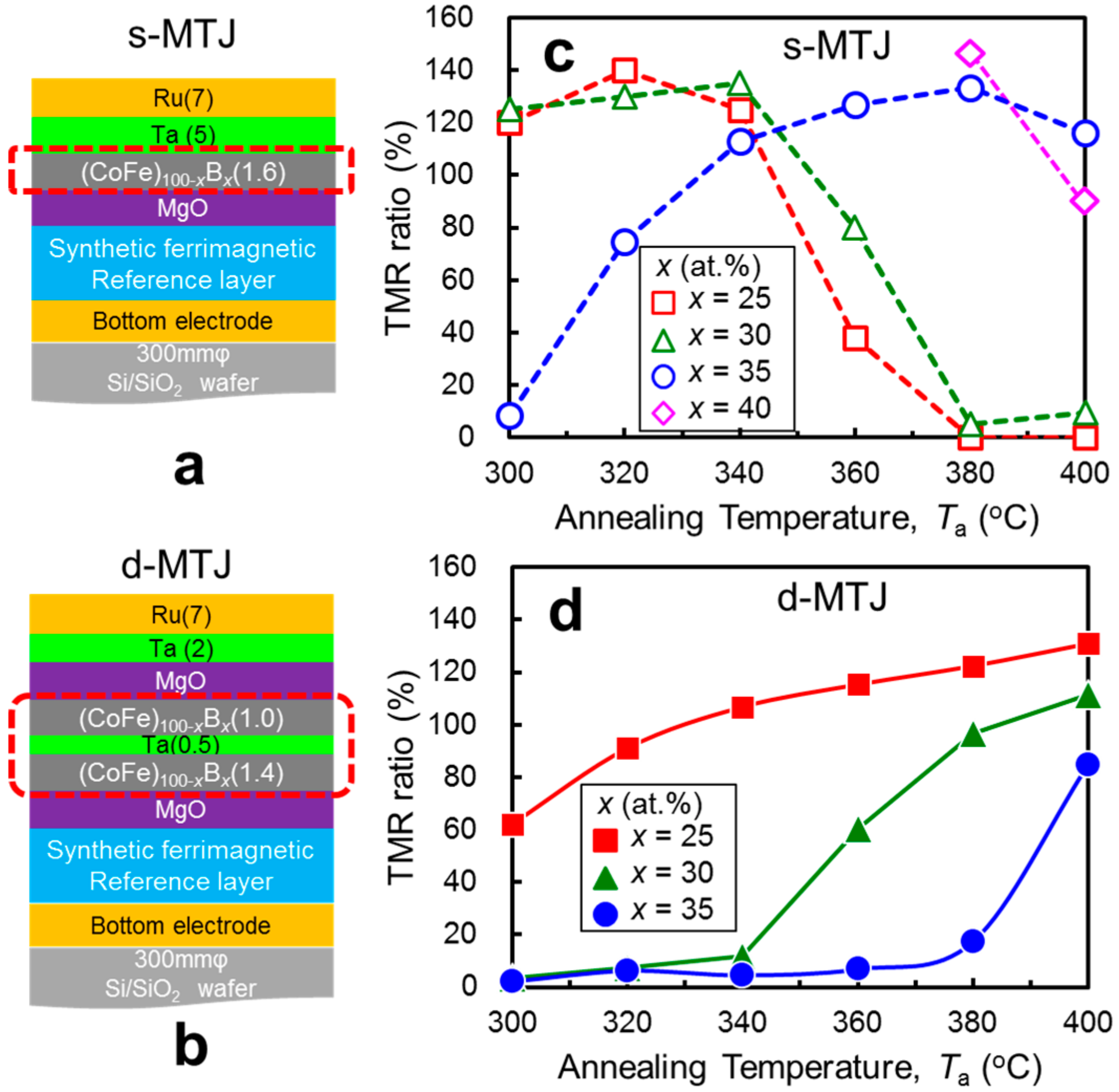
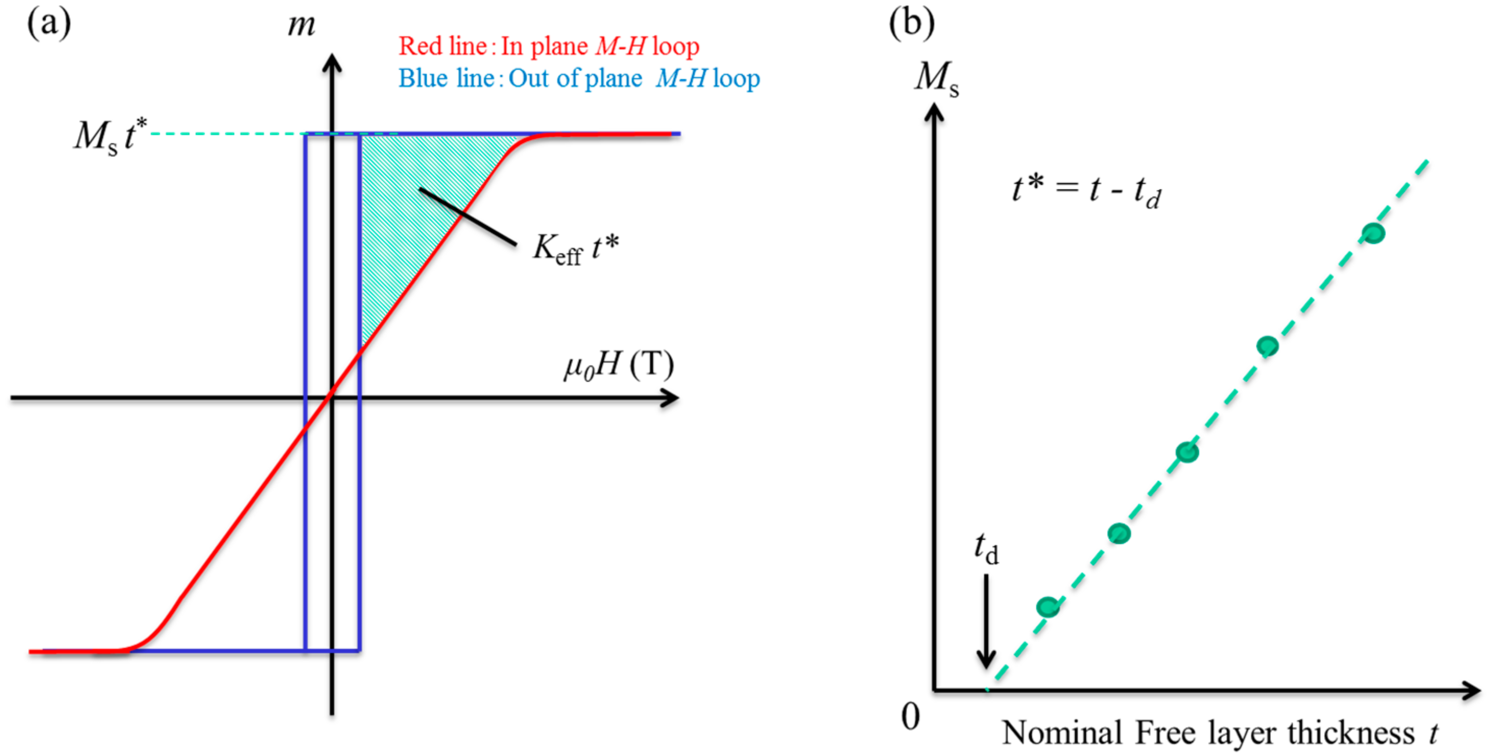
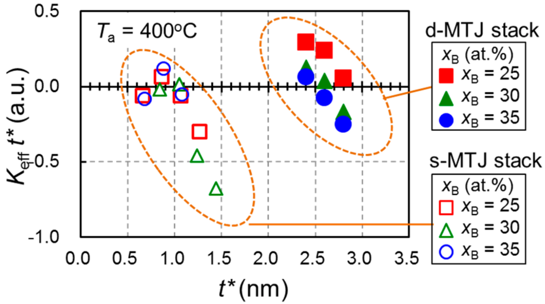
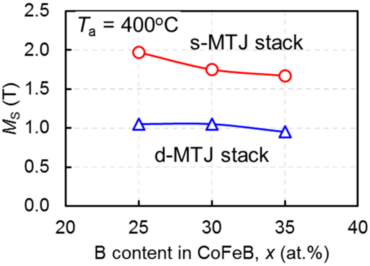
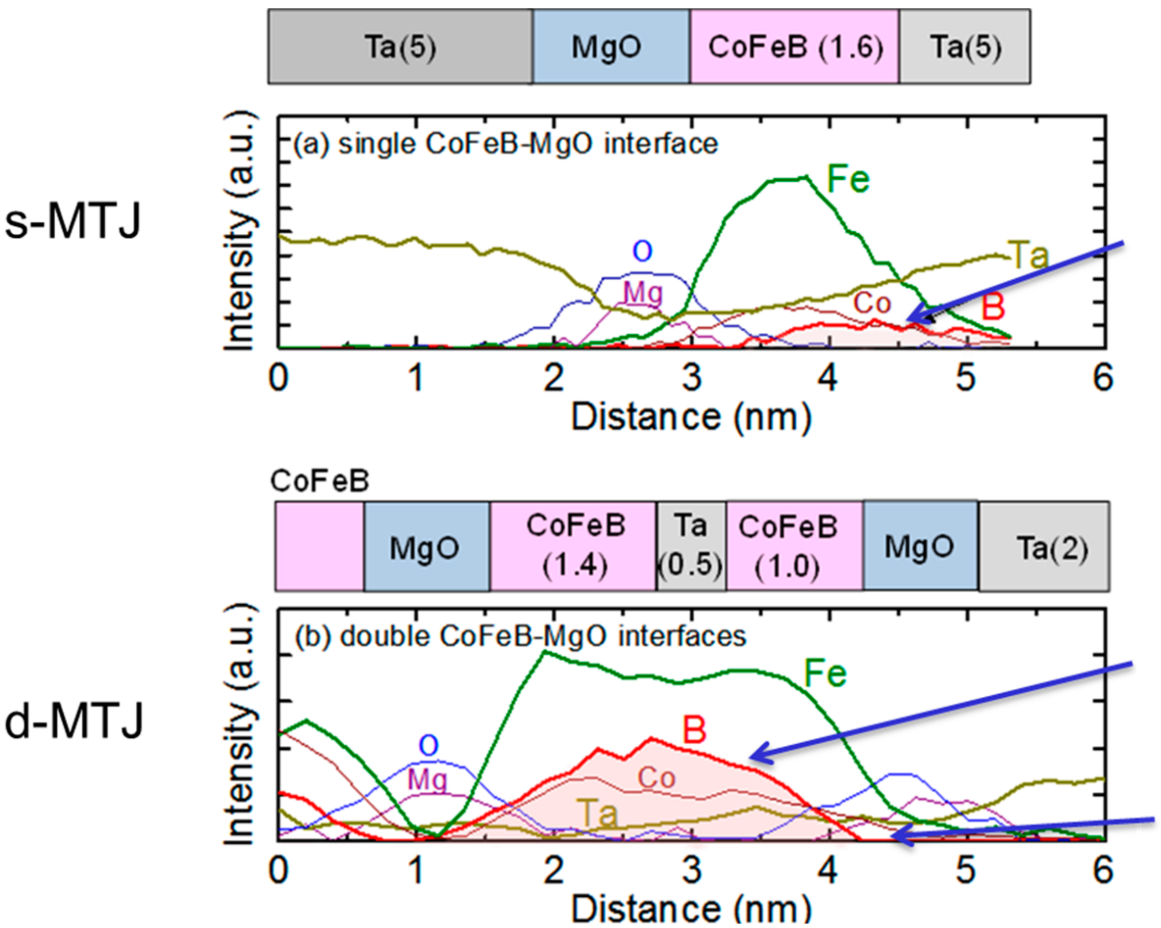
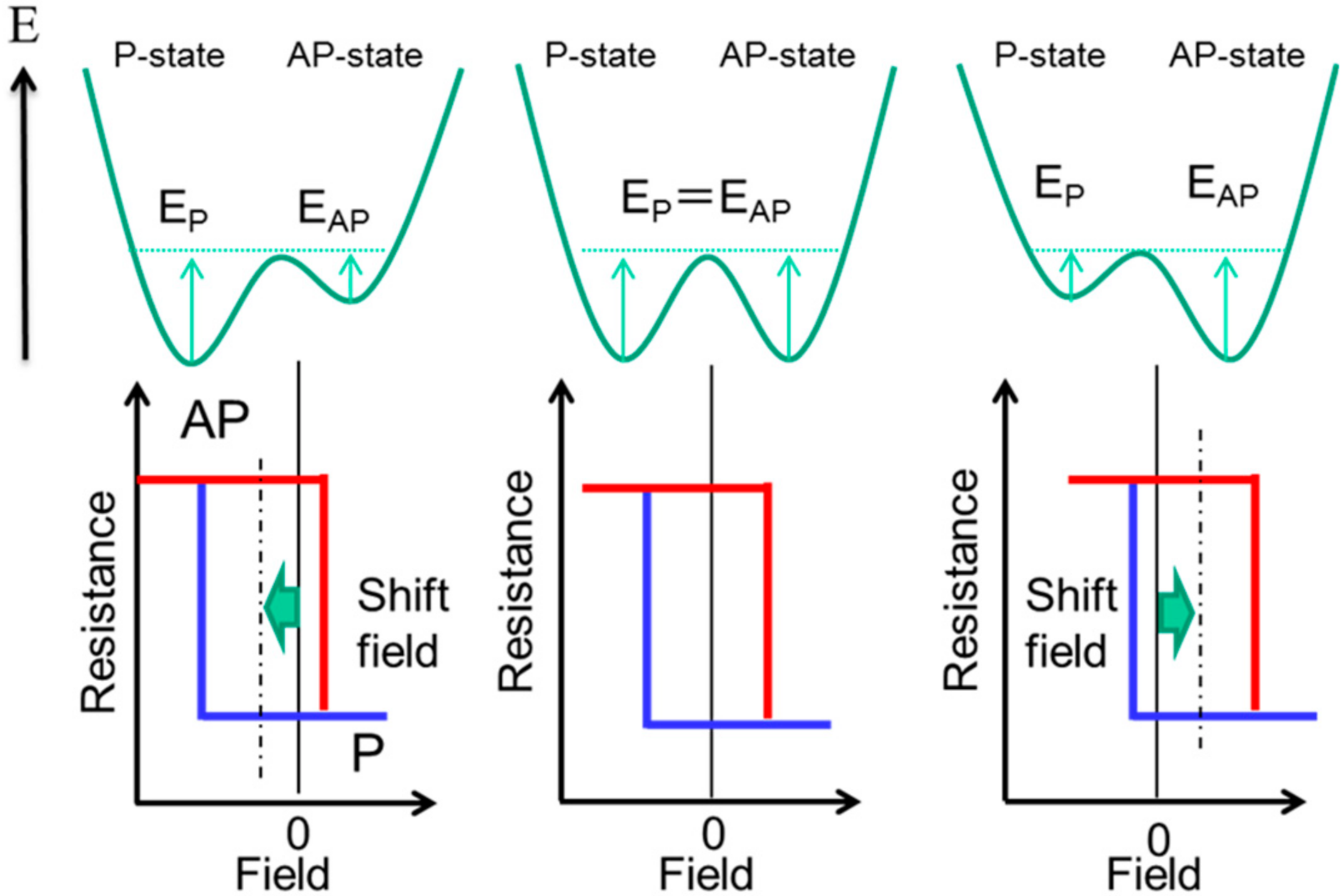
3.1.1. MTJ Design with High Thermal Tolerance for STT-MRAM with CMOS BEOL Process Compatibility

In the MTJs with perpendicular easy axis (p-MTJs) for STT-MRAM, a high tunnel magnetoresistance ratio, low switching current, and high thermal stability are required at the same time. In addition, a large switching field compared to the free layer and a small stray field are required in the reference layer. For integration of STT-MRAM using standard CMOS BEOL process, those properties need to be maintained after annealing at temperature of 400 °C. In order to realize high performance p-MTJ using CoFeB/MgO system showing high tunnel magnetoresistance, a relatively high thermal stability factor, and low switching current [14], Sato et al. proposed MgO/CoFeB/Ta/CoFeB/MgO free layer structure (double CoFeB/MgO interface p-MTJ, d-MTJ) which has larger thermal stability factor than that of MgO/CoFeB/Ta free layer structure (single CoFeB/MgO interface structure, s-MTJ) while maintaining low write current [15,16,17]. We have demonstrated that our developed d-MTJ with a synthetic ferrimagnetic (SyF) reference layer has the capability to withstand annealing at 400 °C in the MTJ diameter down to 10 nm φ [18]. This structure has become de facto standard of p-MTJ.
In order to further improve the p-MTJ performance, one needs to understand the dominant factors in determining thermal tolerance of the p-MTJs. Here, we review our recent progress in the advanced p-MTJs for STT-MRAM. In particular, we describe the material design knowledge of (1) high thermal tolerance by controlling boron composition of CoFeB free layer, (2) damage suppression by sputtering conditions, and (3) thermal tolerance of the reference layer by high-temperature annealing [19,20].
(1) High thermal tolerance by controlling boron composition of CoFeB free layer
To obtain high thermal tolerance, one needs to control diffusion of boron from CoFeB to the adjacent layer because boron concentration plays a crucial role in realizing perpendicular easy axis [18,19,20,21,22,23,24,25,26,27,28,29,30,31,32,33]. As shown in Figure 2a,c, all the s-MTJs showed an increase of TMR ratio up to a specific temperature, above which the TMR ratio degraded. The annealing temperature (Ta) where the maximum TMR ratio is observed in the s-MTJs increases with increasing x up to 35at%B. In s-MTJ with x = 40at%B, the TMR ratio drastically decreases at Ta = 400 °C, which may be related to the formation of a weak (001) texture in MgO/CoFeB stack with high B concentration [30]. On the other hand, as shown in Figure 2b,d, the TMR ratio of d-MTJs increases monotonically as Ta increases up to 400 °C. In d-MTJ with x = 25at%B, TMR ratio reaches to 131%. As x increases, higher Ta is required in order to get a higher TMR ratio. As seen above, the temperature dependence of TMR ratio in d-MTJ is significantly different from that in s-MTJ [29].
To understand the Ta dependence of TMR ratio for s-MTJ and d-MTJ shown in Figure 2, we evaluated effective anisotropy energy density Kefft* from the areal difference between the out-of-plane and in-plane mH curves as shown in Figure 3a. t* is the effective magnetic layer thickness, which is obtained by subtracting the magnetically dead layer thicknesses from the nominal free layer thickness as shown in Figure 3b. Figure 4 shows typical Kefft*-t* plots for the s-MTJ and the d-MTJ with x = 25, 30, and 35at.%B after annealing at Ta = 400 °C. Positive and negative values of Kefft* means in-plane and perpendicular magnetic anisotropy, respectively. In both of s-MTJ and d-MTJ, Kefft* tends to increase as t* decreases. t* indicating the positive value of Kefft* becomes thick in the d-MTJ type compared with s-MTJ. The maximum Kefft* for s-MTJ and d-MTJ annealed at 400 °C is obtained by x = 35 and x = 25, respectively. Thus, high TMR ratios are obtained in s-MTJ and d-MTJ because high perpendicular magnetic anisotropy is realized even in high-temperature annealing at 400 °C.
In the CoFeB/MgO-based p-MTJ system, effective anisotropy energy density Kefft* is determined by competition between interfacial anisotropy Ki and shape anisotropy (−Ms2/2µ0 where MS is saturation magnetization), as expressed in Equation (1).
K e f f t *   =   K i     [ ( N z N x ) M s 2 2 μ 0 + K b ] t *
where Ki is interfacial anisotropy energy, Nz and Nx are demagnetization coefficients, Kb is bulk anisotropy energy. In Equation (1), the second term is shape anisotropy, proportional to Ms square. Kb is negligibly small in the system. Figure 5 shows B content dependence of saturation magnetization Ms evaluated from MH curves for the s-MTJ and d-MTJ annealed at 400 °C. Ms of d-MTJ is suppressed to about half of that of s-MTJ.
From this measured Ms and Equation (1), in the s-MTJ, shape anisotropy is the dominant factor that determines perpendicular anisotropy because of larger Ms (larger shape anisotropy). On the other hand, in the d-MTJ, Ki is the dominant factor because of smaller Ms and larger Ki (about double that of s-MTJ thanks to double CoFeB/MgO interface). In order to improve perpendicular anisotropy, larger Ki and smaller Ms are desirable. However, with increasing B content in CoFeB, both Ms of CoFeB and Ki decreases [21].
The large difference in Ms between s-MTJ and d-MTJ is due to the difference in B diffusion state. As shown in Figure 6, the boron in the s-MTJ adsorbs into the Ta-capping layer. On the other hand, boron in the d-MTJ is located around the Ta insertion layer. The Ta insertion layer acts as a boron absorption layer. Also, the MgO-capping layer blocks boron diffusion from the CoFeB to the Ta-capping layer. As a result, in the d-MTJ, a large amount of boron remains in the CoFeB layer. This results in lower Ms in the free layer of d-MTJ than in that of s-MTJ. These results indicate that boron composition of the CoFeB layer after annealing is a critical factor to realize thermal tolerance for annealing at a temperature of 400 °C, which is a standard requirement for the integration with CMOS in back-end-of line process.
(2) Damage suppression by sputtering conditions
In the double CoFeB–MgO interface structure, a thin metal layer such as Ta, W, or Mo was inserted to absorb boron from the CoFeB layers (MgO/CoFeB/insertion layer/CoFeB/MgO) for high tunnel magnetoresistance (TMR) ratio and perpendicular anisotropy [15,16,29,33,34,35,36,37,38,39,40,41,42,43,44]. First, Ta was used as insertion material because Ta has a bcc crystal structure and is a good boron absorber, as mentioned above. Recently, tungsten (W) was also used as insertion material because W has a higher melting point, resulting in higher thermal stability [39,44].
It was reported that a degree of damage caused by the deposition of heavy metals (Ta or W) on the layer underneath them is generally dependent on sputtering gas species [45,46,47]. In fact, we have revealed that perpendicular anisotropy of the CoFeB–MgO system enhances by using Kr instead of Ar for Ta-capping layer deposition [48]. Because it is important to suppress damage during film deposition for realization of high-performance p-MTJs, it is required to engineer a deposition process for insertion layer resulting in high TMR ratio and high perpendicular anisotropy. Therefore, we evaluated the impact of sputtering condition of W layer in the free layer and the reference layer [49,50]. By using Kr or Xe gas instead of Ar gas for W deposition, TMR ratio and perpendicular anisotropy significantly improved. Energy dispersive X-ray microscope analysis revealed that interdiffusion in the MTJ between, underneath, and on the W was suppressed by using Kr or Xe gas. High-energy recoiled Ar from W sputtering target bombarded the surface of W and underneath the layer. Penetrated Ar may cause large stress and defects in the film, resulting in larger interdiffusion in the film. In fact, Ar was observed in W(Ar) while Kr and Xe were not in W(Kr) and W(Xe) [49].
(3) Thermal tolerance of the reference layer by high-temperature annealing
As mentioned in the previous section, we have demonstrated the thermal tolerance against 400 °C annealing in CoFeB–MgO-based p-MTJs with the Co/Pt multilayer-based SyF reference layer [17].
However, we simultaneously observed a variation of shift field Hs caused by an uncompensated stray magnetic field from the reference layer as annealing temperature Ta increased from 350 °C to 400 °C [18], resulting in asymmetry of thermal stability factor Δ between parallel (P) and antiparallel (AP) states, as shown in Figure 7 [18].
To clarify the origin of the variation of Hs, we investigated Ta dependence of spontaneous magnetic moment per unit area ms of each layer in reference layer (Figure 8) and a variation of composition depth profile after annealing at 400 °C.
We investigated properties of the p-MTJ at elevated annealing temperature Ta from 350 °C to 400 °C. The MTJs annealed at 400 °C show larger Hs (AP state becomes more stable) compared to those annealed at 350 °C. The variation of Hs resulted because the ms of top Co/Pt multilayer with CoFeB insertion layer decreased and the ms of bottom Co/Pt multilayer decreased as Ta increased from 350 °C to 400 °C. EDX line analysis revealed that Fe in the CoFeB layer underneath the MgO layer (in the reference layer) diffuses into Co/Pt multilayers in the SyF reference layer via annealing at Ta = 400 °C, which could cause the variation of ms in the SyF reference layer. The results indicate that suppression of Fe diffusion in the CoFeB layer in the reference layer is important to achieve more robust MTJs against annealing.
In order to overcome this issue, we have developed surface modification process (SMT) on the Pt buffer layer by ion irradiation [20]. SMT improves crystallinity of the Co/Pt multilayer even after 400 °C annealing, resulting in high perpendicular anisotropy of Co/Pt and suppression of Fe diffusion in the CoFeB reference layer [20].

3.1.2. Recent Progress of STT-MRAMs

As mentioned earlier, STT-MRAMs are attracting much attention owing to their high potential to offer electronics with both low-power consumption and high performance for IoT and AI applications. Recently, many researchers and fab companies have focused on STT-MRAM using CoFeB/MgO-based p-MTJ because STT-MRAM with p-MTJ is the most promising emerging memory in terms of scalability, high write endurances, high operation speed, and CMOS back-end-of-line process compatibility. We have successfully developed prototype high-speed operation 6T-2MTJ STT-MRAM, 1T-1MTJ STT-MRAM with on-via MTJ (see Figure 9), and so on [51,52]. A Gbit-class, large-capacity MRAM was also published by SK Hynix & Toshiba [53]. Three megafab companies have announced that the risk of mass production of the STT-MRAM will be started in 2018, where the STT-MRAM will be in place of either eFlash or SRAM [54,55,56]. For the scalability, the patterning method of MTJ has to change from ion beam etching (IBE) to reactive ion etching (RIE). However, IBE is still used because RIE of magnetic material is not easy. In order to apply RIE to MTJ etching, new etching chemistry and methods are needed. We have developed low-damage and short-failure-free RIE technologies for STT-MRAM [57]. By replacing MTJ etching technology from IBE to RIE, it can be expected to realize high density STT-MRAM for DRAM substitution.

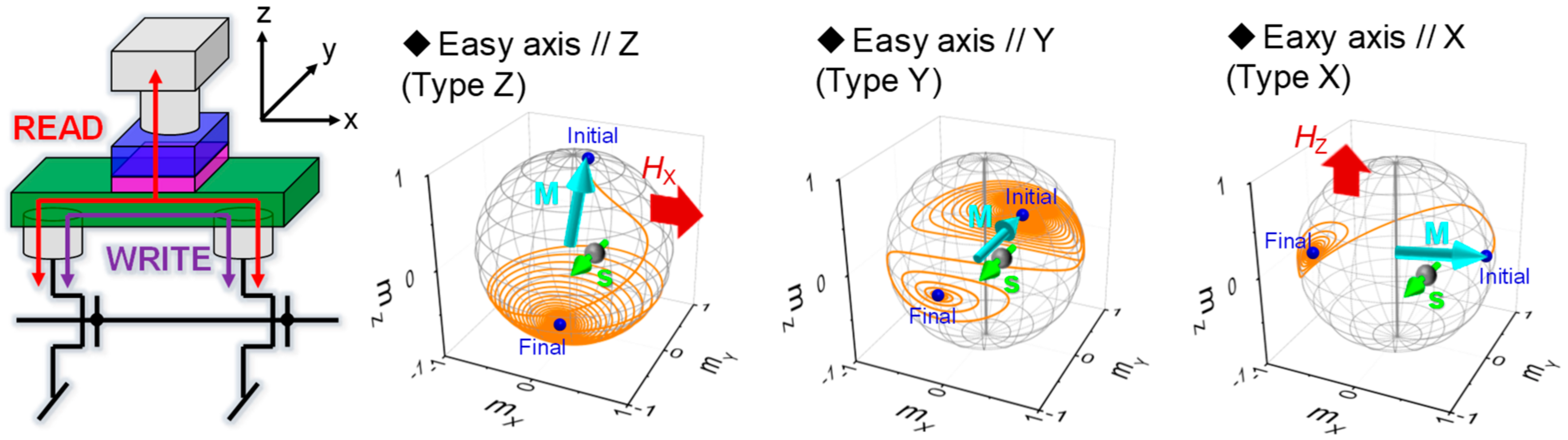
3.2. Progress of SOT-MRAM and Future Issues for NV Memory Applications

As shown in Figure 1b, in the memory cell of SOT-MRAM, the MTJ is fabricated on the channel layer, which is made of heavy metal, such as Ta, W, Hf, and so on, in order to have higher spin-orbit torque [6,7,58,59,60,61,62,63,64,65]. There are three types of SOT devices (called type x, type y, and type z) where the relationship between magnetization easy axis direction and channel current direction differs [66]. Figure 10 shows a schematic diagram of the three types of SOT devices. In each figure, the magnetization trajectory during switching is also shown. Among the three types of devices, magnetic-field-free switching can be achieved in only the y-type, while in the other two devices, one needs to apply either in-plane or out-of-plane field for z-type and x-type devices, respectively. However, the y-type device shows similar switching trajectory to that in the conventional STT device, resulting in a steep increase in switching current as the write pulse width reduces down to ns regime. Therefore, from the viewpoint of high-speed writing operation, the x-type and z-type devices are much preferable. In order to eliminate external magnetic field for z-type, exchange bias field is employed by putting antiferromagnetic material underneath the free layer, which can play a role as a channel layer generating SOT [62]. The field-free switching has been demonstrated in Hall-bar devices with z-type devices, but not in the actual SOT device for NV memory. Toward the NV memory applications, the field-free switching needs to be demonstrated with thermal tolerance against annealing at 400 °C in the actual SOT device for NV memory, which is a standard requirement for CMOS BEOL, as mentioned in the former section. For the x-type device, the field-free switching has also been demonstrated by tilting easy axis angle from x-axis in the actual SOT device for memory applications [67], thus we focus on how it can be done in this review paper.
Figure 11a shows the SOT device structure demonstrating field-free switching. In the x-type device, the direction of spin generated by the channel layer is orthogonal to the easy axis of magnetization in the free layer, therefore, in order to switch it, one needs to break the symmetry. One way to break the symmetry is applying the out-of-plane field, which is not suitable for LSIs. The other way is canting the easy axis of magnetization from the x-axis, by which the direction of spin generated by the channel layer is not orthogonal to the easy axis of magnetization, resulting in the symmetry breaking. Figure 11b shows resistance versus current density curve of the SOT device.
Where the easy axis of magnetization is parallel to the major axis of ellipse, θ is varied from 0 (x-type) to ±15° with respect to the x-axis. To switch the magnetization in the x-type device with θ = 0°, a small out-of-plane field is necessary, whereas the switching can be observed in the device with θ = ±15° in an absence of the out-of-plane field. The results demonstrate that the field-free switching can be achieved in the SOT device.
Hereafter we focus on a few issues in SOT devices to be addressed for NV memory applications. As shown in Table 1, one of the advantages of SOT devices is high potential in realizing high-speed writing operation comparable to SRAM. In order to make it clear whether the SOT device can be used in place of SRAM at low-level cache, it is necessary to confirm its high-speed operation capability at LSI level. So far, at the device level, high-speed switching down to 500 ps has been demonstrated. However, at LSI level, one needs to consider operation speed of CMOS circuits, which is necessary for driving the SOT-MRAM, including addressing and write driver, and so on. In addition to that, the read operation needs to be confirmed at LSI level. Another issue is high writing current, which is one order of magnitude larger than that of the STT-MRAM. To reduce the writing current in the SOT-MRAM, the material of the channel layer needs to be developed such that higher SOT can be obtained. So far, high resistivity W channel is preferable for it as the high spin Hall angle can be achieved. The spin Hall angle θSH is defined as θSH = JS/Je where Je and JS are applied charge current density flowing through the channel layer and a resultant transverse-flowing spin current density, respectively. A quantitative measurement method of θSH is summarized in [68].
However, high-resistivity channel layer material deteriorates the drivability of the selective transistor, resulting in an enlargement of cell size. For lowering writing current without sacrificing drivability of the selective transistor, it is required to develop the channel layer material with low resistivity while high spin Hall angle is maintained. The last issue is scaling of the SOT device. In this review, we have mainly introduced the SOT device with in-plane-type MTJs. In the in-plane MTJs, the magnetic anisotropy originates from shape anisotropy, which will become smaller as the device dimensions reduce when the free layer thickness is fixed. One option to address this issue is the introduction of perpendicular anisotropy material (z-type device). Thus, it is very important to develop perpendicular-anisotropy MTJs with the thermal tolerance against annealing at 400 °C at least using a top reference layer fabricated on the channel layer with high spin Hall angle, while some engineering needs to be introduced such that the field-free switching can be achieved. By addressing those issues, the SOT device will be very attractive for replacement of SRAM in a lower-level cache memory.

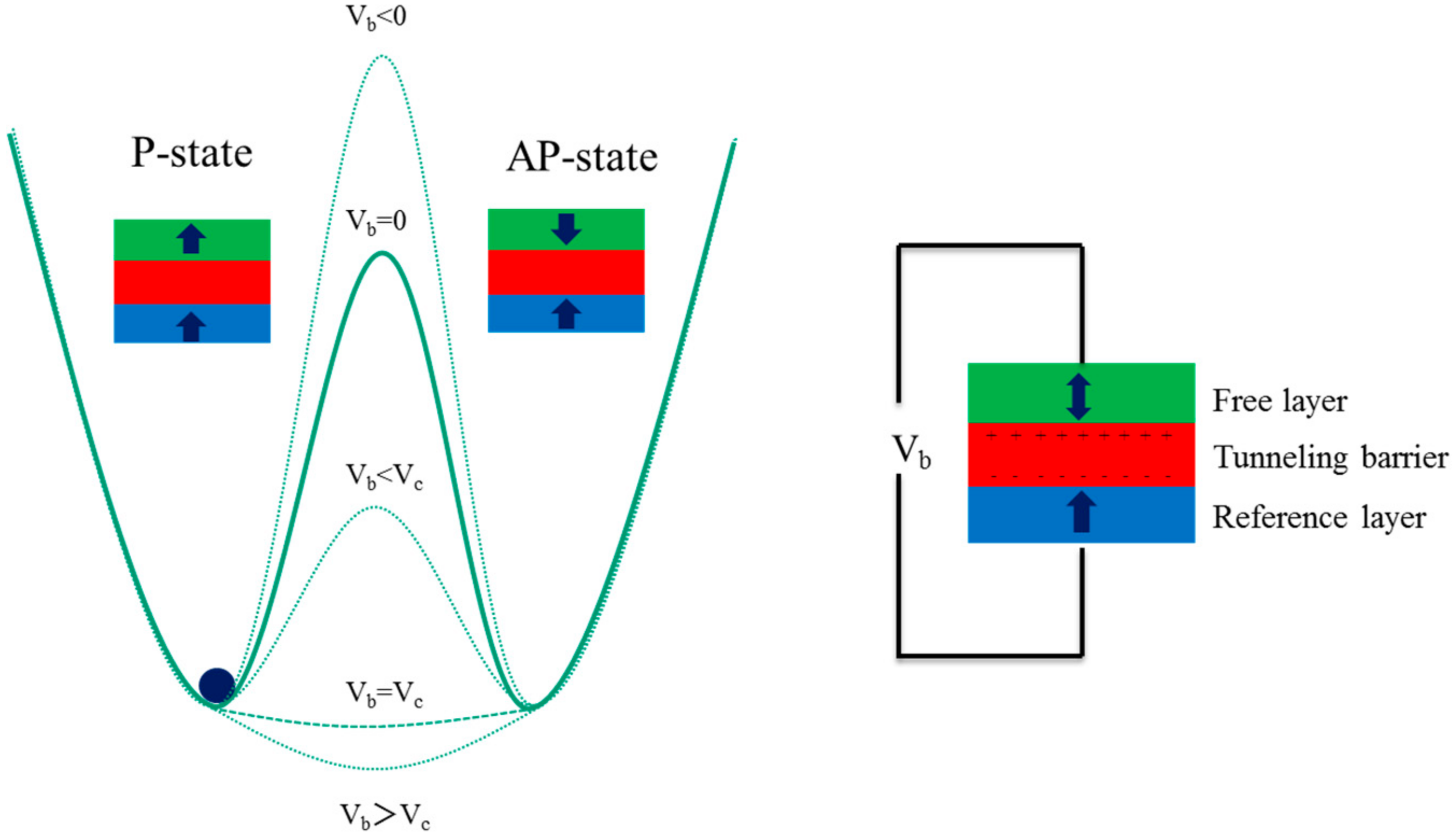
3.3. Progress of VC-MRAM

As mentioned in the introduction, the writing scheme for VC-MRAM is electric-field effect on (or voltage-controlled) magnetic anisotropy. An electric-field effect on magnetic properties have been first demonstrated in magnetic semiconductors such as (In,Mn)As and (Ga,Mn)As. In the magnetic semiconductors, the modulation of the Curie temperature, coercivity, magnetic anisotropy, and anomalous Hall coefficient has been observed [69,70,71,72]. Those studies have triggered the following intensive studies on the modulation of the magnetic properties in metals [73,74,75,76,77,78,79,80,81,82,83,84,85,86]. From memory application viewpoint, one significant breakthrough for E-field effect on metal is found in the demonstration of switching in the MTJ device [77,78,79]. In particular, Kanai et al. demonstrated the E-field-induced magnetization switching in perpendicular-anisotropy CoFeB/MgO system [79], which is de facto standard material system for the STT-MRAM.
Figure 12 illustrates the writing operation principle of voltage-controlled MRAM VC-MRAM. In VC-MRAM, a magnetic anisotropy modulation by electric field (voltage) is utilized. By applying the external voltage Vb, the interfacial perpendicular magnetic anisotropy of the p-MTJ is modulated [87], resulting in the change of energy barrier depth between P and AP state. When Vb is negative (positive), interfacial perpendicular anisotropy increases (decreases). At above threshold voltage, precessional switching can be achieved under magnetic field.
Although significant developments have been done in VC-MRAM, there are still some issues for practical use in NV memory. One issue is that the required voltage to switch the magnetization is large compared with standard CMOS power-supply voltage. For example, Noguchi et al. reported VC-MRAM circuits for ultralarge last level cache memory, in which the voltage to switch the magnetization is as high as 2.2 V [10], which is larger than the standard CMOS power-supply voltage of less than 1.2 V. The necessity of such a large voltage originates from limited amounts of anisotropy modulation coefficients by E-field. To overcome this issue, the material development of the free-layer material is now underway [88,89,90,91,92]. Another issue to be addressed is the small time window for the writing. Since the precessional motion of magnetization is utilized in the VC-MRAM, the switching probability oscillates with respect to the write pulse width, resulting in the small writing-time window. One possible solution for this issue is combining E-field-induced switching with STT [93]. In addition to the issued raised above, it is necessary to engineer elimination of external magnetic field for precessional switching. In the papers reported so far, the external magnetic field along in-plane or out-of-plane direction is applied to induce the precessional switching. Because it is difficult to equip the external magnetic field in the LSIs, one needs to consider other schemes to induce the precessional switching without the external magnetic field.
Although there are a few issues in VC-MRAM to be addressed for practical NV memory applications, the E-field effect on magnetic anisotropy itself becomes useful for spintronics-based NV memory. Yoda et al. reported the possibility in reducing the memory cell size of SOT-MRAM by fabricating multiple MTJs on one channel layer, in which each MTJ can be independently switched by making use of E-field modulation of the magnetic anisotropy [94].

Author Contributions

T.E. and H.H. wrote the manuscript. All authors reviewed the final manuscript.

Funding

This research was supported by the Center for Innovative Integrated Electronic Systems Industrial Affiliation on STT-MRAM program, JST-ACCEL, ImPACT of CSTI, and JST-OPERA.

Acknowledgments

The authors thank Ohno, H., Fukami, S., and S. Kanai for fruitful discussion.

Conflicts of Interest

The authors declare no conflict of interest.

Glossary

BEOLback-end-of-line
MTJmagnetic tunneling junctions
MRAMmagnetic random access memory
SOTspin-orbit torque
STTspin-transfer torque
VCvoltage controlled

References

  1. Ohno, H.; Endoh, T.; Hanyu, T.; Kasai, N.; Ikeda, S. Magnetic Tunnel Junction for Nonvolatile CMOS Logic. In Proceedings of the 2010 International Electron Devices Meeting 2010, San Francisco, CA, USA, 6–8 December 2010; p. 218. [Google Scholar] [CrossRef]
  2. Endoh, T.; Koike, H.; Ikeda, S.; Hanyu, T.; Ohno, H. An Overview of Nonvolatile Emerging Memories—Spintronics for Working Memories. IEEE J. Emerg. Sel. Top. Circ. Syst. 2016, 6, 109–119. [Google Scholar] [CrossRef]
  3. Hanyu, T.; Endoh, T.; Suzuki, D.; Koike, H.; Ma, Y.; Onizawa, N.; Natsui, M.; Ikeda, S.; Ohno, H. Standby-Power-Free Integrated Circuits Using MTJ-Based VLSI Computing. Proc. IEEE 2016, 104, 1844–1863. [Google Scholar] [CrossRef]
  4. Slonczewski, J.C. Current-driven excitation of magnetic multilayers. J. Magn. Magn. Mater. 1996, 159, L1–L7. [Google Scholar] [CrossRef]
  5. Berger, L. Emission of spin waves by a magnetic multilayer traversed by a current. Phys. Rev. B 1996, 54, 9353. [Google Scholar] [CrossRef]
  6. Liu, L.; Pai, C.-F.; Li, Y.; Tseng, H.W.; Ralph, D.C.; Buhrman, R.A. Spin-Torque Switching with the Giant Spin Hall Effect of Tantalum. Science 2012, 336, 555–558. [Google Scholar] [CrossRef] [PubMed] [Green Version]
  7. Miron, I.M.; Garello, K.; Gaudin, G.; Zermatten, P.J.; Costache, M.V.; Auffret, S.; Bandiera, S.; Rodmacq, B.; Schuhl, A.; Gambardella, P. Perpendicular switching of a single ferromagnetic layer induced by in-plane current injection. Nature 2011, 476, 189–193. [Google Scholar] [CrossRef] [PubMed]
  8. Chernyshov, A.; Overby, M.; Liu, X.; Furdyna, J.K.; Lyanda-Geller, Y.; Rokhinson, L.P. Evidence for reversible control of magnetization in a ferromagnetic material by means of spin–orbit magnetic field. Nat. Phys. 2009, 5, 656–659. [Google Scholar] [CrossRef] [Green Version]
  9. Rizal, C.; Moa, B.; Niraula, B.B. Ferromagnetic Multilayers: Magnetoresistance, Magnetic Anisotropy, and Beyond. Magnetochemistry 2016, 2, 22. [Google Scholar] [CrossRef]
  10. Noguchi, H.; Ikegami, K.; Abe, K.; Fujita, S.; Shiota, Y.; Nozaki, T.; Yuasa, S.; Suzuki, Y. Novel Voltage Controlled MRAM (VCM) with Fast Read/Write Circuits for Ultra Large Last Level Cache. In Proceedings of the 2016 IEEE International Electron Devices Meeting (IEDM), San Francisco, CA, USA, 3–7 December 2016; p. 4. [Google Scholar]
  11. Kang, S.H.; Park, C. MRAM: Enabling a Sustainable Device for Pervasive System Architectures and Applications. In Proceedings of the 2017 IEEE International Electron Devices Meeting (IEDM), San Francisco, CA, USA, 2–6 December 2017; p. 4. [Google Scholar]
  12. Maurelli, A. Embedded Non Volatile Memories for Automotive applications. In Proceedings of the Short Course of International Electron Devices Meeting, San Francisco, CA, USA, 5–7 December 2017. [Google Scholar]
  13. Shum, P.D. Embedded MRAM Technology for IoT & Automotive. In Proceedings of the Short Course of International Electron Devices Meeting, San Francisco, CA, USA, 5–7 December 2017. [Google Scholar]
  14. Ikeda, S.; Miura, K.; Yamamoto, H.; Mizunuma, K.; Gan, H.D.; Endo, M.; Kanai, S.; Hayakawa, J.; Matsukura, F.; Ohno, H. A perpendicular-anisotropy CoFeB-MgO magnetic tunnel junction. Nat. Mater. 2010, 9, 721–724. [Google Scholar] [CrossRef] [PubMed]
  15. Sato, H.; Yamanouchi, M.; Ikeda, S.; Fukami, S.; Matsukura, F.; Ohno, H. Perpendicular-anisotropy CoFeB-MgO magnetic tunnel junctions with a MgO/CoFeB/Ta/CoFeB/MgO recording structure. Appl. Phys. Lett. 2012, 101, 022414. [Google Scholar] [CrossRef]
  16. Sato, H.; Enobio, E.C.I.; Yamanouchi, M.; Ikeda, S.; Fukami, S.; Kanai, S.; Matsukura, F.; Ohno, H. Properties of magnetic tunnel junctions with a MgO/CoFeB/Ta/CoFeB/MgO recording structure down to junction diameter of 11 nm. Appl. Phys. Lett. 2014, 105, 062403. [Google Scholar] [CrossRef]
  17. Sato, H.; Ikeda, S.; Fukami, S.; Honjo, H.; Ishikawa, S.; Yamanouchi, S.; Mizunuma, K.; Matsukura, S.; Ohno, H. Co/Pt multilayer based reference layers in magnetic tunnel junctions for nonvolatile spintronics VLSIs. Jpn. J. Appl. Phys. 2014, 53, 04EM02. [Google Scholar] [CrossRef]
  18. Honjo, H.; Sato, H.; Ikeda, S.; Sato, S.; Watanabe, T.; Miura, S.; Nasuno, T.; Noguchi, Y.; Yasuhira, M.; Tanigawa, T.; et al. 10 nmf perpendicular-anisotropy CoFeB-MgO magnetic tunnel junction with over 400 °C high thermal tolerance by boron diffusion control. In Proceedings of the 2015 Symposium on VLSI Technology (VLSI Technology), Kyoto, Japan, 16–18 June 2015; pp. T160–T161. [Google Scholar] [CrossRef]
  19. Honjo, H.; Ikeda, S.; Sato, H.; Watanabe, T.; Miura, S.; Nasuno, T.; Noguchi, Y.; Yasuhira, M.; Tanigawa, T.; Koike, H.; et al. Origin of variation of shift field via annealing at 400 °C in a perpendicular-anisotropy magnetic tunnel junction with [Co/Pt]-multilayers based synthetic ferrimagnetic reference layer. AIP Adv. 2017, 7, 055913. [Google Scholar] [CrossRef]
  20. Honjo, H.; Ikeda, S.; Sato, S.; Nishioka, K.; Watanabe, T.; Miura, S.; Nasuno, T.; Noguchi, Y.; Inoue, H.; Yasuhira, M.; et al. High thermal tolerance synthetic ferrimagnetic reference layer with modified buffer layer by ion irradiation for perpendicular anisotropy magnetic tunnel junctions. In Proceedings of the 2018 IEEE International Magnetic Conference (INTERMAG), Singapore, 23–27 April 2018; p. HC-05. [Google Scholar]
  21. Ikeda, S.; Koizumi, R.; Sato, H.; Yamanouchi, S.; Miura, K.; Mizunuma, K.; Gan, H.; Matsukura, S.; Ohno, H. Boron Composition Dependence of Magnetic Anisotropy and Tunnel Magnetoresistance in MgO/CoFe(B) Based Stack Structures. IEEE. Trans. Magn. 2012, 48, 3829–3832. [Google Scholar] [CrossRef]
  22. Watanabe, K.; Ishikawa, S.; Sato, H.; Ikeda, S.; Yamanouchi, S.; Fukami, S.; Matsukura, S.; Ohno, H. Dependence of magnetic properties of MgO/CoFeB/Ta stacks on CoFeB and Ta thicknesses. Jpn. J. Appl. Phys. 2015, 54, 04DM04. [Google Scholar] [CrossRef]
  23. Miyajima, T.; Ibusuki, T.; Umehara, T.; Sato, M.; Eguchi, S.; Tsukada, M.; Kataoka, Y. Transmission electron microscopy study on the crystallization and boron distribution of CoFeB/MgO/CoFeB magnetic tunnel junctions with various capping layers. Appl. Phys. Lett. 2009, 94, 122501. [Google Scholar] [CrossRef]
  24. Karthik, S.V.; Takahashi, Y.K.; Ohkubo, T.; Ikeda, S.; Ohno, H. Transmission electron microscopy investigation of CoFeB/MgO/CoFeB pseudospin valves annealed at different temperatures. J. Appl. Phys. 2009, 94, 023920. [Google Scholar] [CrossRef]
  25. Ikeda, S.; Hayakawa, J.; Lee, Y.M.; Tanikawa, T.; Matsukura, S.; Ohno, H. Tunnel magnetoresistance in MgO-barrier magnetic tunnel junctions with bcc-CoFe(B) and fcc-CoFe free layers. J. Appl. Phys. 2006, 99, 08A907. [Google Scholar] [CrossRef]
  26. Sinha, J.; Hayashi, M.; Kellock, A.J.; Fukami, S.; Yamanouchi, S.; Sato, H.; Ikeda, S.; Mitani, S.; Yang, S.-H.; Parkin, S.S.P.; et al. Enhanced interface perpendicular magnetic anisotropy in Ta|CoFeB|MgO using nitrogen doped Ta underlayers. Appl. Phys. Lett. 2013, 102, 242405. [Google Scholar] [CrossRef] [Green Version]
  27. Gan, H.D.; Ikeda, S.; Shiga, W.; Hayakawa, J.; Miura, K.; Yamamoto, H.; Hasegawa, H.; Matsukura, S.; Ohkubo, T.; Hono, K.; et al. Tunnel magnetoresistance properties and film structures of double MgO barrier magnetic tunnel junctions. Appl. Phys. Lett. 2010, 96, 192507. [Google Scholar] [CrossRef]
  28. Feng, G.; Dijken, S.V.; Feng, J.F.; Coey, J.M.D.; Leo, T.; Smith, D.J. Annealing of CoFeB/MgO based single and double barrier magnetic tunnel junctions: Tunnel magnetoresistance, bias dependence, and output voltage. J. Appl. Phys. 2009, 105, 033916. [Google Scholar] [CrossRef] [Green Version]
  29. Honjo, H.; Ikeda, S.; Sato, H.; Sato, S.; Watanabe, T.; Miura, S.; Nasuno, T.; Noguchi, Y.; Yasuhira, M.; Tanigawa, T.; et al. Improvement of thermal tolerance of CoFeB-MgO perpendicular-anisotropy magnetic tunnel junctions by controlling boron composition. IEEE. Trans. Magn. 2016, 52, 340110. [Google Scholar] [CrossRef]
  30. Kodzuka, M.; Ohkubo, T.; Hono, K.; Ikeda, S.; Gan, H.D.; Ohno, H. Effects of boron composition on tunneling magnetoresistance ratio and microstructure of CoFeB/MgO/CoFeB pseudo-spin-valve magnetic tunnel junctions. J. Appl. Phys. 2012, 111, 043913. [Google Scholar] [CrossRef]
  31. Watanabe, K.; Fukami, S.; Sato, H.; Ikeda, S.; Matsukura, S.; Ohno, H. Annealing temperature dependence of magnetic properties of CoFeB/MgO stacks on different buffer layers. Jpn. J. Appl. Phys. 2017, 56, 0802B2. [Google Scholar] [CrossRef] [Green Version]
  32. Xu, X.D.; Mukaiyama, K.; Kasai, S.; Ohkubo, T.; Hono, K. Impact of boron diffuision at MgO grain boundaries on magneto-transport properties of MgO/CoFeB/W magnetic tunnel junctions. Acta Mater. 2018, 161, 360–366. [Google Scholar] [CrossRef]
  33. Iwata-Harms, J.M.; Jan, G.; Liu, H.; Serrano-Guisan, S.; Zhu, J.; Thomas, L.; Tong, R.-Y.; Sunder, V.; Wang, P.-K. High-temperature thermal stability driven by magnetization dilution in CoFeB free layers for spin-transfer-torque magnetic random access memory. Sci. Rep. 2018, 8, 14409. [Google Scholar] [CrossRef] [PubMed]
  34. Kim, W.; Couet, S.; Swerts, J.; Lin, T.; Tomczak, Y.; Souriau, L.; Tsvetanova, D.; Sankaran, K.; Donadio, G.L.; Crotti, D.; et al. Experimental Observation of Back-Hopping with Reference layer Flipping by High-Voltage Pulse in Perpendicular Magnetic Tunnel Junctions. IEEE. Trans. Magn. 2016, 52, 3401004. [Google Scholar] [CrossRef]
  35. Goff, A.L.; Garcia, K.; Vernier, N.; Tahmasebi, T.; Cornelissen, S.; Min, T.; Devolder, T. Effect of Ta insertion in Reference Layers of MTJs With Perpendicular Anisotoropy. IEEE Trans. Magn. 2014, 50. [Google Scholar] [CrossRef]
  36. Goff, A.L.; Soucaille, R.; Tahmasebi, T.; Swerts, J.; Furnemont, A.; Devolder, T. Optimization of top-pinned perpendicular anisotropy tunnel junctions through Ta insertion. Jpn. J. Appl. Phys. 2015, 54, 090302. [Google Scholar] [CrossRef]
  37. Cuchet, L.; Rodmacq, B.; Auffret, S.; Sousa, R.; Ducruet, C.; Dieny, B. Influence of a Ta spacer on the magnetic and transport properties of perpendicular magnetic tunnel junctions. Appl. Phys. Lett. 2013, 103, 052402. [Google Scholar] [CrossRef]
  38. Couet, S.; Devolver, T.; Swerts, J.; Mertens, S.; Lin, T.; Liu, E.; Elshocht, S.V.; Kar, G.S. Impact of Ta and W-based spacers in double MgO STT-MRAM free layers on perpendicular anisotoropy and damping. Appl. Phys. Lett. 2017, 111, 152406. [Google Scholar] [CrossRef]
  39. Lee, D.-Y.; Hong, S.-H.; Lee, S.-E.; Park, J.-G. Dependency of Tunneling-Magnetoresistance Ratio on Nanoscale Spacer Thickness and Material for Double MgO Based Perpendicular-Magnetic-Tunneling-Junction. Nat. Sci. Rep. 2016, 6, 38125. [Google Scholar] [CrossRef] [PubMed] [Green Version]
  40. Kim, J.-H.; Lee, J.-B.; An, G.-G.; Yang, S.-M.; Chung, W.-S.; Park, H.-S.; Hong, J.-P. Ultrathin W space layer-enabled thermal stability enhancement in a perpendicular MgO/CoFeB/W/CoFeB/MgO recording frame. Nat. Sci. Rep. 2015, 5, 16903. [Google Scholar] [CrossRef] [PubMed] [Green Version]
  41. Lee, S.-E.; Shim, T.-H.; Park, J.-G. Perpendicular magnetic tunnel junction (p-MTJ) spin-valves designed with a top Co2Fe6B2 free layer and a nanoscale-thick tungsten bridging and capping layer. NPG Asia Mater. 2016, 8, e324. [Google Scholar] [CrossRef]
  42. Chatterjee, J.; Sousa, R.C.; Perrissin, N.; Auffret, S.; Ducruet, C.; Dieny, B. Enhanced annealing stability and perpendicular magnetic anisotropy in perpendicular magnetic tunnel junctions using W layer. Appl. Phys. Lett. 2017, 110, 202401. [Google Scholar] [CrossRef]
  43. Choi, J.Y.; Lee, D.-G.; Baek, J.-U.; Park, J.-G. Double MgO-based Perpendicular Magnetic-Tunnel-Junction Spin-valve Structure with a Top Co2Fe6B2 Free Layer using a Single SyAF [Co/Pt]n Layer. Nat. Sci. Rep. 2018, 8, 2139. [Google Scholar] [CrossRef] [PubMed]
  44. Wang, M.; Cai, W.; Cao, K.; Zhou, J.; Wrona, J.; Peng, S.; Yang, H.; Wei1, J.; Kang, W.; Zhang, Y.; et al. Current-induced magnetization switching in atom thick tungsten engineered perpendicular magnetic tunnel junctions with large tunnel magnetoresistance. Nat. Commun. 2018, 9, 671. [Google Scholar] [CrossRef] [PubMed]
  45. Winters, H.F.; Coufal, H.J. Influence of energy reflected from the target on thin film characteristics. J. Vac. Sci. Technol. A 1993, 11, 657–663. [Google Scholar] [CrossRef]
  46. Iwatsubo, S.; Takahashi, T.; Naoe, M. Magnetic properties of Fe films deposited by Ar, Kr, and Xe ion beam sputtering. J. Appl. Phys. 1998, 83, 6667–6669. [Google Scholar] [CrossRef]
  47. Maeda, Y.; Suzuki, Y.; Sakashima, Y.; Iwata, S.; Kato, S.; Tsunashima, S.; Toyoda, H.; Sugai, I. Effect of sputtering Deposition Process on Magnetic Properties of Magnetic CoPt multilayer. Jpn. J. Appl. Phys. 2008, 47, 7879–7885. [Google Scholar] [CrossRef]
  48. Honjo, H.; Fukami, S.; Ishihara, K.; Nebashi, R.; Kinoshita, K.; Tokutome, K.; Murahata, M.; Miura, S.; Sakimura, N.; Sugibayashi, T.; et al. Three-terminal magnetic tunneling junction device with perpendicular anisotropy CoFeB sensing layer. J. Appl. Phys. 2014, 115, 17B750. [Google Scholar] [CrossRef]
  49. Honjo, H.; Ikeda, S.; Sato, H.; Nishioka, K.; Watanabe, T.; Miura, S.; Nasuno, T.; Noguchi, Y.; Yasuhira, M.; Tanigawa, T.; et al. Impact of tungsten sputtering condition on magnetic and transport properties of double-MgO magnetic tunneling junction with CoFeB/W/CoFeB free layer. IEEE Trans. Magn. 2017, 53, 2501604. [Google Scholar] [CrossRef]
  50. Honjo, H.; Ikeda, S.; Sato, H.; Yasuhira, M.; Endoh, T. Critical role of W insertion layer sputtering condition for reference layer on magnetic and transport properties of perpendicular-anisotropy magnetic tunnel junction. In Proceedings of the Joint MMM and International Magnetic Conference, Washington, DC, USA, 14–18 January 2019. [Google Scholar]
  51. Ohsawa, T.; Miura, S.; Kinoshita, K.; Honjo, H.; Ikeda, S.; Hanyu, T.; Ohno, H.; Endoh, T. A 1.5nsec/2.1nsec random read/write cycle 1Mb STT-RAM using 6T2MTJ cell with background write for nonvolatile e-memories. In Proceedings of the 2013 Symposium on VLSI Circuits, Kyoto, Japan, 12–14 June 2013; pp. 110–111. [Google Scholar]
  52. Koike, H.; Miura, S.; Honjo, H.; Watanabe, T.; Sato, H.; Sato, S.; Nasuno, T.; Noguchi, Y.; Yasuhira, M.; Tanigawa, T.; et al. 1T1MTJ STT-MRAM Cell Array Design with an Adaptive Reference Voltage Generator for Improving Device Variation Tolerance. In Proceedings of the 2015 IEEE International Memory Workshop (IMW), Monterey, CA, USA, 17–20 May 2015; pp. 141–144. [Google Scholar] [CrossRef]
  53. Chung, S.-W.; Kishi, T.; Park, J.W.; Yoshikawa, M.; Park, K.S.; Nagase, T.; Sunouchi, K.; Kanaya, H.; Kim, G.C.; Noma, K.; et al. 4Gbit density STT-MRAM using perpendicular MTJ realized with compact cell structure. In Proceedings of the 2016 IEEE International Electron Devices Meeting (IEDM), San Francisco, CA, USA, 3–7 December 2016; pp. 659–662. [Google Scholar] [CrossRef]
  54. Kang, S.H. Embedded STT-MRAM for Energy-efficient and Cost-effective Mobile Systems. In Proceedings of the 2014 Symposium on VLSI Technology (VLSI-Technology): Digest of Technical Papers, Honolulu, HI, USA, 9–12 June 2014; pp. 44–45. [Google Scholar] [CrossRef]
  55. Lee, K.; Yamane, K.; Noh, S.; Naik, V.B.; Yang, H.; Jang, S.H.; Kwon, J.; Behin-Aein, B.; Chao, R.; Lim, J.H.; et al. 22-nm FD-SOI Embedded MRAM with Full Solder Reflow Compatibility and Enhanced Magnetic Immunity. In Proceedings of the 2018 IEEE Symposium on VLSI Technology, Honolulu, HI, USA, 18–22 June 2018; pp. 183–184. [Google Scholar]
  56. Lee, Y.K.; Song, Y.; Kim, J.C.; Oh, S.C.; Bae, B.-J.; Lee, S.H.; Le, J.H.; Pi, U.H.; Seo, B.; Jung, H.; et al. Embedded STT-MRAM in 28-nm FDSOI Logic Process for Industrial MCU/IoT Application. In Proceedings of the VLSI Symposium on Technology, Honolulu, HI, USA, 18–22 June 2018; pp. 181–182. [Google Scholar]
  57. Sato, H.; Watanabe, T.; Koike, H.; Saito, T.; Miura, S.; Honjo, H.; Inoue, H.; Ikeda, S.; Noguchi, Y.; Tanigawa, T.; et al. 1T-1MTJ type embedded STT-MRAM with advanced low-damage and short-failure-free RIE technology down to 32 nmφ MTJ patterning. In Proceedings of the 2018 IEEE International Memory Workshop (IMW), Kyoto, Japan, 13–16 May 2018; pp. 135–138. [Google Scholar] [CrossRef]
  58. Pai, C.-F.; Liu, L.; Li, Y.; Tseng, H.W.; Ralph, D.C.; Buhrman, R.A. Spin transfer torque devices utilizing the giant spin Hall effect of tungsten. Appl. Phys. Lett. 2012, 101, 122404. [Google Scholar] [CrossRef] [Green Version]
  59. Yamanouchi, M.; Chen, L.; Kim, J.; Hayashi, M.; Sato, H.; Fukami, S.; Ikeda, S.; Matsukura, F.; Ohno, H. Three terminal magnetic tunnel junction utilizing the spin Hall effect of iridium-doped copper. Appl. Phys. Lett. 2013, 102, 212408. [Google Scholar] [CrossRef]
  60. Fan, Y.; Upadhyaya, P.; Kou, X.; Lang, M.; Takei, S.; Wang, Z.; Tang, J.; He, L.; Chang, L.T.; Montazeri, M.; et al. Magnetization switching through giant spin-orbit torque in a magnetically doped topological insulator heterostructure. Nat. Mater. 2014, 13, 699–704. [Google Scholar] [CrossRef] [PubMed]
  61. Akyol, M.; Yu, G.; Alzate, J.G.; Upadhyaya, P.; Li, X.; Wong, K.L.; Ekicibil, A.; Khalili Amiri, P.; Wang, K.L. Current-induced spin-orbit torque switching of perpendicularly magnetized Hf|CoFeB|MgO and Hf|CoFeB|TaOx structures. Appl. Phys. Lett. 2015, 106, 162409. [Google Scholar] [CrossRef]
  62. Fukami, S.; Zhang, C.; DuttaGupta, S.; Kurenkov, A.; Ohno, H. Magnetization switching by spin-orbit torque in an antiferromagnet-ferromagnet bilayer system. Nat. Mater. 2016, 15, 535–541. [Google Scholar] [CrossRef] [PubMed]
  63. Oh, Y.W.; Chris Baek, S.H.; Kim, Y.M.; Lee, H.Y.; Lee, K.D.; Yang, C.G.; Park, E.S.; Lee, K.S.; Kim, K.W.; Go, G.; et al. Field-free switching of perpendicular magnetization through spin-orbit torque in antiferromagnet/ferromagnet/oxide structures. Nat. Nanotechnol. 2016, 11, 878–884. [Google Scholar] [CrossRef] [PubMed]
  64. Fukami, S.; Ohno, H. Magnetization switching schemes for nanoscale three-terminal spintronics devices. Jpn. J. Appl. Phys. 2017, 56, 0802A0801. [Google Scholar] [CrossRef]
  65. Takeuchi, Y.; Zhang, C.; Okada, A.; Sato, H.; Fukami, S.; Ohno, H. Spin-orbit torques in high-resistivity-W/CoFeB/MgO. Appl. Phys. Lett. 2018, 112, 192408. [Google Scholar] [CrossRef] [Green Version]
  66. Fukami, S.; Anekawa, T.; Zhang, C.; Ohno, H. A spin-orbit torque switching scheme with collinear magnetic easy axis and current configuration. Nat. Nanotechnol. 2016, 11, 621–625. [Google Scholar] [CrossRef] [PubMed]
  67. Fukami, S.; Anekawa, T.; Zhang, C.; Ohno, H. A sub-ns three-terminal spin-orbit torque induced switching device. In Proceedings of the 2016 IEEE Symposium on VLSI Technology, Honolulu, HI, USA, 14–16 June 2016; p. 2. [Google Scholar]
  68. Lau, Y.-C.; Hayashi, M. Spin torque efficiency of Ta, W, and Pt in metallic bilayers evaluated by harmonic Hall and spin Hall magnetoresistance measurements. Jpn. J. Applied. Phys. 2017, 56, 0802B5. [Google Scholar] [CrossRef] [Green Version]
  69. Ohno, H.; Chiba, D.; Matsukura, F.; Omiya, T.; Abe, E.; Dietl, T.; Ohno, Y.; Ohtani, K. Electric-field control of ferromagnetism. Nature 2000, 408, 944–946. [Google Scholar] [CrossRef] [PubMed]
  70. Chiba, D.; Yamanouchi, M.; Matsukura, F.; Ohno, H. Electrical Manipulation of Magnetization Reversal in a Ferromagnetic Semiconductor. Science 2003, 301, 943–945. [Google Scholar] [CrossRef] [PubMed]
  71. Chiba, D.; Sawicki, M.; Nishitani, Y.; Nakatani, Y.; Matsukura, F.; Ohno, H. Magnetization vector manipulation by electric fields. Nature 2008, 455, 515–518. [Google Scholar] [CrossRef] [PubMed]
  72. Chiba, D.; Werpachowska, A.; Endo, M.; Nishitani, Y.; Matsukura, F.; Dietl, T.; Ohno, H. Anomalous Hall Effect in Field-Effect Structures of (Ga,Mn)As. Phys. Rev. Lett. 2010, 104, 106601. [Google Scholar] [CrossRef] [PubMed] [Green Version]
  73. Weisheit, M.; Fahler, S.; Marty, A.; Souche, Y.; Poinsignon, C.; Givord, D. Electric Field–Induced Modification of Magnetism in Thin-Film Ferromagnets. Science 2007, 315, 349–351. [Google Scholar] [CrossRef] [PubMed]
  74. Maruyama, T.; Shiota, Y.; Nozaki, T.; Ohta, K.; Toda, N.; Mizuguchi, M.; Tulapurkar, A.A.; Shinjo, T.; Shiraishi, M.; Mizukami, S.; et al. Large voltage-induced magnetic anisotropy change in a few atomic layers of iron. Nat. Nanotechnol. 2009, 4, 158–161. [Google Scholar] [CrossRef] [PubMed]
  75. Endo, M.; Kanai, S.; Ikeda, S.; Matsukura, F.; Ohno, H. Electric-field effects on thickness dependent magnetic anisotropy of sputtered MgO/Co40Fe40B20/Ta structures. Appl. Phys. Lett. 2010, 96, 212503. [Google Scholar] [CrossRef]
  76. Zhernenkov, M.; Fitzsimmons, M.R.; Chlistunoff, J.; Majewski, J.; Tudosa, I.; Fullerton, E.E. Electric-field modification of magnetism in a thin CoPd film. Phys. Rev. B 2010, 82, 024420. [Google Scholar] [CrossRef]
  77. Shiota, Y.; Nozaki, T.; Bonell, F.; Murakami, S.; Shinjo, T.; Suzuki, Y. Induction of coherent magnetization switching in a few atomic layers of FeCo using voltage pulses. Nat. Mater. 2011, 11, 39–43. [Google Scholar] [CrossRef] [PubMed]
  78. Wang, W.G.; Li, M.; Hageman, S.; Chien, C.L. Electric-field-assisted switching in magnetic tunnel junctions. Nat. Mater. 2011, 11, 64–68. [Google Scholar] [CrossRef] [PubMed]
  79. Kanai, S.; Yamanouchi, M.; Ikeda, S.; Nakatani, Y.; Matsukura, F.; Ohno, H. Electric field-induced magnetization reversal in a perpendicular-anisotropy CoFeB-MgO magnetic tunnel junction. Appl. Phys. Lett. 2012, 101, 122403. [Google Scholar] [CrossRef]
  80. Nozaki, T.; Shiota, Y.; Miwa, S.; Murakami, S.; Bonell, F.; Ishibashi, S.; Kubota, H.; Yakushiji, K.; Saruya, T.; Fukushima, A.; et al. Electric-field-induced ferromagnetic resonance excitation in an ultrathin ferromagnetic metal layer. Nat. Phys. 2012, 8, 491–496. [Google Scholar] [CrossRef]
  81. Kanai, S.; Gajek, M.; Worledge, D.C.; Matsukura, F.; Ohno, H. Electric field-induced ferromagnetic resonance in a CoFeB/MgO magnetic tunnel junction under dc bias voltages. Appl. Phys. Lett. 2014, 105, 242409. [Google Scholar] [CrossRef]
  82. Okada, A.; Kanai, S.; Yamanouchi, M.; Ikeda, S.; Matsukura, F.; Ohno, H. Electric-field effects on magnetic anisotropy and damping constant in Ta/CoFeB/MgO investigated by ferromagnetic resonance. Appl. Phys. Lett. 2014, 105, 052415. [Google Scholar] [CrossRef]
  83. Ando, F.; Kakizakai, H.; Koyama, T.; Yamada, K.; Kawaguchi, M.; Kim, S.; Kim, K.J.; Moriyama, T.; Chiba, D.; Ono, T. Modulation of the magnetic domain size induced by an electric field. Appl. Phys. Lett. 2016, 109, 022401. [Google Scholar] [CrossRef] [Green Version]
  84. Dohi, T.; Kanai, S.; Okada, A.; Matsukura, F.; Ohno, H. Effect of electric-field modulation of magnetic parameters on domain structure in MgO/CoFeB. AIP Adv. 2016, 6, 075017. [Google Scholar] [CrossRef] [Green Version]
  85. Dohi, T.; Kanai, S.; Matsukura, F.; Ohno, H. Electric-field effect on spin-wave resonance in a nanoscale CoFeB/MgO magnetic tunnel junction. Appl. Phys. Lett. 2017, 111, 072403. [Google Scholar] [CrossRef]
  86. Kanai, S.; Matsukura, F.; Ohno, H. Electric-field-induced magnetization switching in CoFeB/MgO magnetic tunnel junctions. Jpn. J. Appl. Phys. 2017, 56, 0802A0803. [Google Scholar] [CrossRef]
  87. Duan, C.G.; Velev, J.P.; Sabirianov, R.F.; Zhu, Z.; Chu, J.; Jaswal, S.S.; Tsymbal, E.Y. Surface magnetoelectric effect in ferromagnetic metal films. Phys. Rev. Lett. 2008, 101, 137201. [Google Scholar] [CrossRef] [PubMed]
  88. Skowroński, W.; Nozaki, T.; Lam, D.D.; Shiota, Y.; Yakushiji, K.; Kubota, H.; Fukushima, A.; Yuasa, S.; Suzuki, Y. Underlayer material influence on electric-field controlled perpendicular magnetic anisotropy in CoFeB/MgO magnetic tunnel junctions. Phys. Rev. B 2015, 91, 184410. [Google Scholar] [CrossRef]
  89. Nozaki, T.; Kozioł-Rachwał, A.; Skowroński, W.; Zayets, V.; Shiota, Y.; Tamaru, S.; Kubota, H.; Fukushima, A.; Yuasa, S.; Suzuki, Y. Large Voltage-Induced Changes in the Perpendicular Magnetic Anisotropy of an MgO-Based Tunnel Junction with an Ultrathin Fe Layer. Phys. Rev. Appl. 2016, 5, 044006. [Google Scholar] [CrossRef]
  90. Nozaki, T.; Kozioł-Rachwał, A.; Tsujikawa, M.; Shiota, Y.; Xu, X.; Ohkubo, T.; Tsukahara, T.; Miwa, S.; Suzuki, M.; Tamaru, S.; et al. Highly efficient voltage control of spin and enhanced interfacial perpendicular magnetic anisotropy in iridium-doped Fe/MgO magnetic tunnel junctions. NPG Asia Mater. 2017, 9, e451. [Google Scholar] [CrossRef] [Green Version]
  91. Xiang, Q.; Wen, Z.; Sukegawa, H.; Kasai, S.; Seki, T.; Kubota, T.; Takanashi, K.; Mitani, S. Nonlinear electric field effect on perpendicular magnetic anisotropy in Fe/MgO interfaces. J. Phys. D Appl. Phys. 2017, 50, 40LT04. [Google Scholar] [CrossRef] [Green Version]
  92. Nozaki, T.; Yamamoto, T.; Tamaru, S.; Kubota, H.; Fukushima, A.; Suzuki, Y.; Yuasa, S. Enhancement in the interfacial perpendicular magnetic anisotropy and the voltage-controlled magnetic anisotropy by heavy metal doping at the Fe/MgO interface. APL Mater. 2018, 6, 026101. [Google Scholar] [CrossRef]
  93. Kanai, S.; Nakatani, Y.; Yamanouchi, M.; Ikeda, S.; Sato, H.; Matsukura, F.; Ohno, H. Magnetization switching in a CoFeB/MgO magnetic tunnel junction by combining spin-transfer torque and electric field-effect. Appl. Phys. Lett. 2014, 104, 212406. [Google Scholar] [CrossRef]
  94. Yoda, H.; Shimomura, N.; Ohsawa, Y.; Shioiri, S.; Kato, Y.; Inokuchi, T.; Kamiguchi, Y.; Altansargai, B.; Saito, Y.; Koi, K.; et al. Voltage-Control Spintronics Memory (VoCSM) Having Potentials of Ultra-Low Energy-Consumption and High-Density. In Proceedings of the 2016 IEEE International Electron Devices Meeting (IEDM), San Francisco, CA, USA, 3–7 December 2016. [Google Scholar]
Figure 1. (a) Memory cell structure for STT-MRAM and VC-MRAM. The memory cell structure consisting of one magnetic tunnel junction (MTJ) and one transistor yields in minimum cell size. There are many variations for the memory cell structure depending on the applications, in particular, for the STT-MRAM. (b) Memory cell structure for SOT-MRAM, where one MTJ and two transistors are required at least.
Jlpea 08 00044 g001
Figure 2. Schematic for single CoFeB–MgO interface MTJ (s-MTJ) (a) and double CoFeB–MgO interface MTJ (d-MTJ) (b) stack structures. Annealing temperature Ta dependence of tunnel magnetoresistance (TMR) ratio for s-MTJ (c) and d-MTJ (d) with B content of 25–40at. % in CoFeB free layer.
Jlpea 08 00044 g002
Figure 3. Magnetic moment per unit area versus in-plane and out-of-plane magnetic field (a) and saturation magnetization Ms versus nominal free layer thickness t (b).
Jlpea 08 00044 g003
Figure 4. Kefft* as a function of t* for s-MTJ and d-MTJ with B content of 25–35at.% annealed at 400 °C.
Jlpea 08 00044 g004
Figure 5. B content dependence of saturation magnetization Ms for s-MTJ and d-MTJ with B content of 25–35at% annealed at 400 °C.
Jlpea 08 00044 g005
Figure 6. EELS line profiles of B, Fe, Co, Ta, Mg, and O elements for s-MTJ and d-MTJ annealed at 400 °C.
Jlpea 08 00044 g006
Figure 7. Schematic for potential curve at parallel (P) and antiparallel (AP) state (a) and resistance versus magnetic field curve. Shift field Hs is defined as center of hysteresis curve.
Jlpea 08 00044 g007
Figure 8. (a) Stack structure of a stack for magnetic tunnel junction (MTJ). (b) Magnetic moment per unit area versus magnetic field curve of the stack MTJ. Arrows show a direction of magnetic moment for free layer msfree, top part of reference layer msref1, and bottom part of reference layer msref2.
Jlpea 08 00044 g008
Figure 9. Microphotograph of 1Mb 6T2MTJ STT-MRAM (a) and 2Mb 1T1MTJ STT-MRAM (b).
Jlpea 08 00044 g009
Figure 10. Schematic diagrams of three types of SOT devices in which magnetization trajectory during switching is also shown as inset.
Jlpea 08 00044 g010
Figure 11. (a) SOT device structure for field-free switching where the easy axis of magnetization, parallel to the major axis of ellipse, θ is canted from the x-axis. (b) Resistance versus current density curve for the SOT device with θ = 0° (x-type) and 15°.
Jlpea 08 00044 g011
Figure 12. Schematic diagrams of writing operation principle of voltage-controlled MRAM (VC-MRAM).
Jlpea 08 00044 g012
Table 1. Benchmarking results of STT-MAM, SOT-MRAM, and VC-MRAM as NV memories using spintronics devices compared with SRAM and eFlash as CMOS-based memories. The F denotes feature size of CMOS. Memory cell size is defined by F.
SRAMSTT-MRAM for SRAMeFlashSTT-MRAM for eFlashSOT-MRAMVC-MRAM
Cell size160–200 F270–100 F240 F250–60 F2160 F250–60 F2
Operation voltage (V)0.6–1.20.6≥100.60.62.2
Write current (A)10−510−510−510−510−410−5
R/W time (ns)≤2/≤25/1010/20,00025/2005/≤210/≤2
RetentionVolatile1 month>20 years15 years≤10 years1 month
Endurance (cycles)101610141051081014-

