A 0.5 V 68 nW ECG Monitoring Analog Front-End for Arrhythmia Diagnosis


Abstract
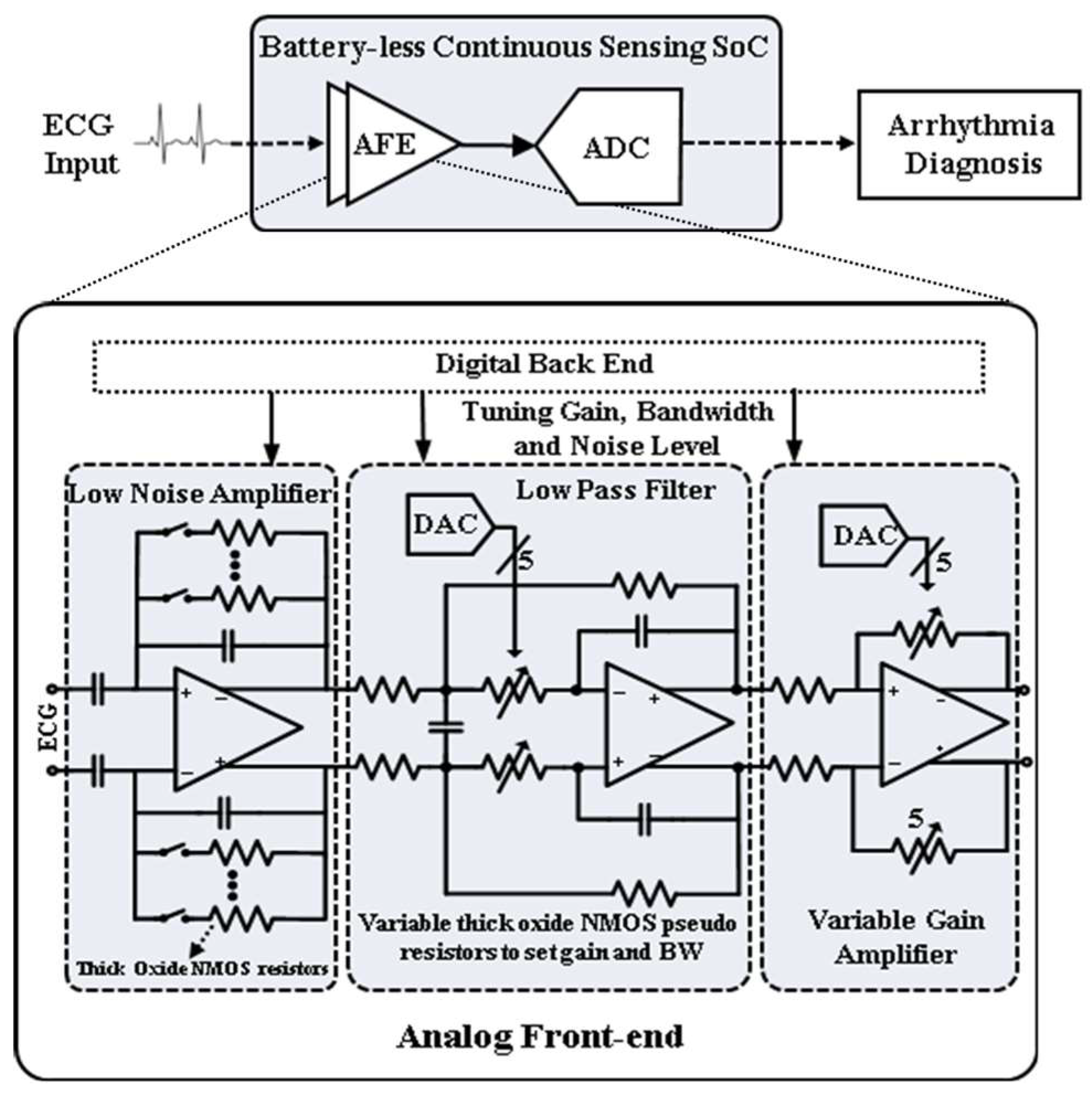
:1. Introduction
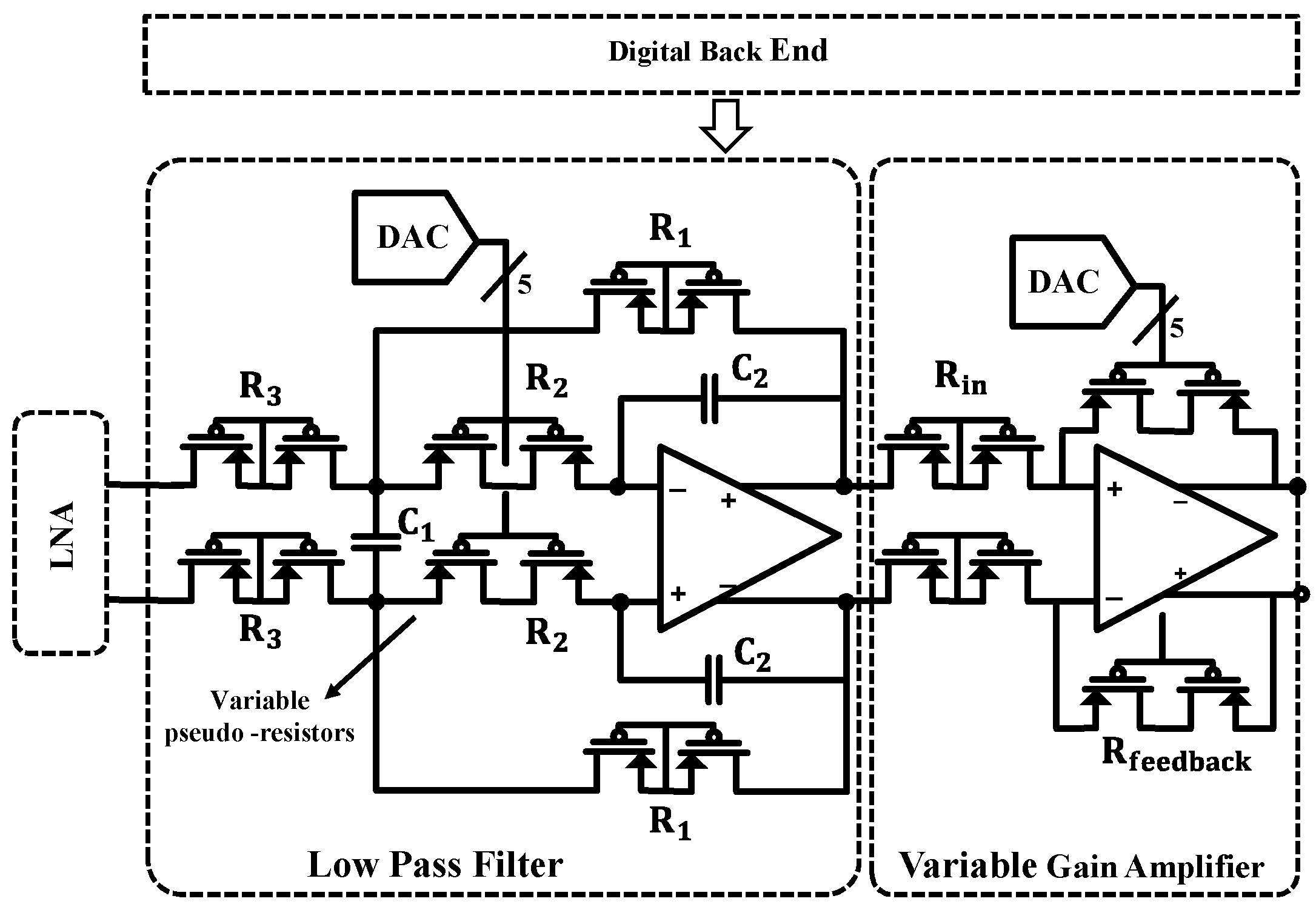
2. AFE Architecture
3. Low-Noise Amplifier Design
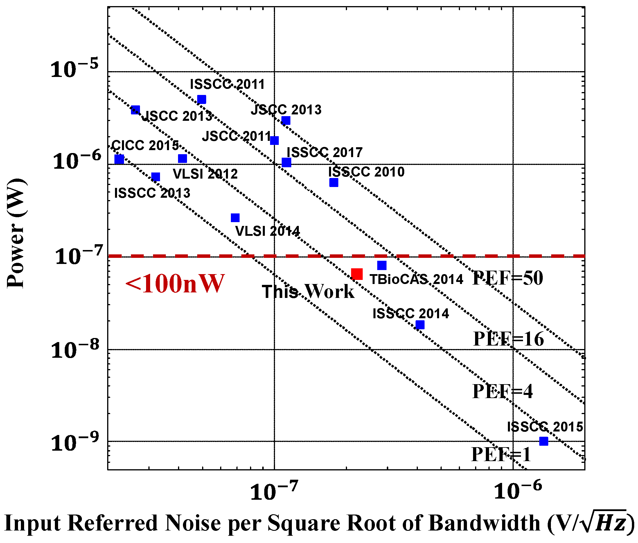
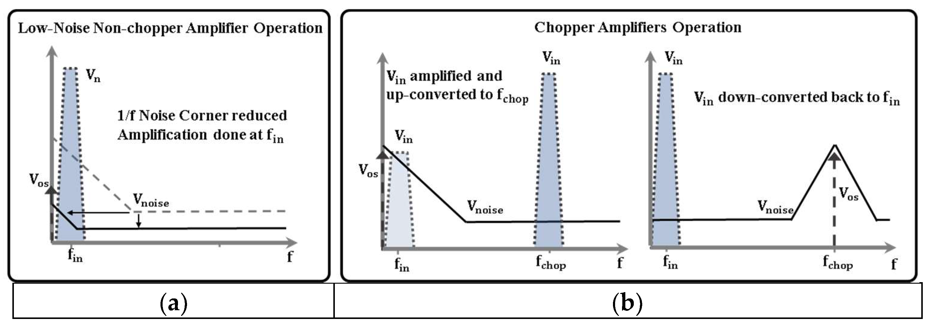
3.1. State-of-the-Art Biopotential Low-Noise Amplifiers
3.2. Low-Power Low-Noise Amplifier
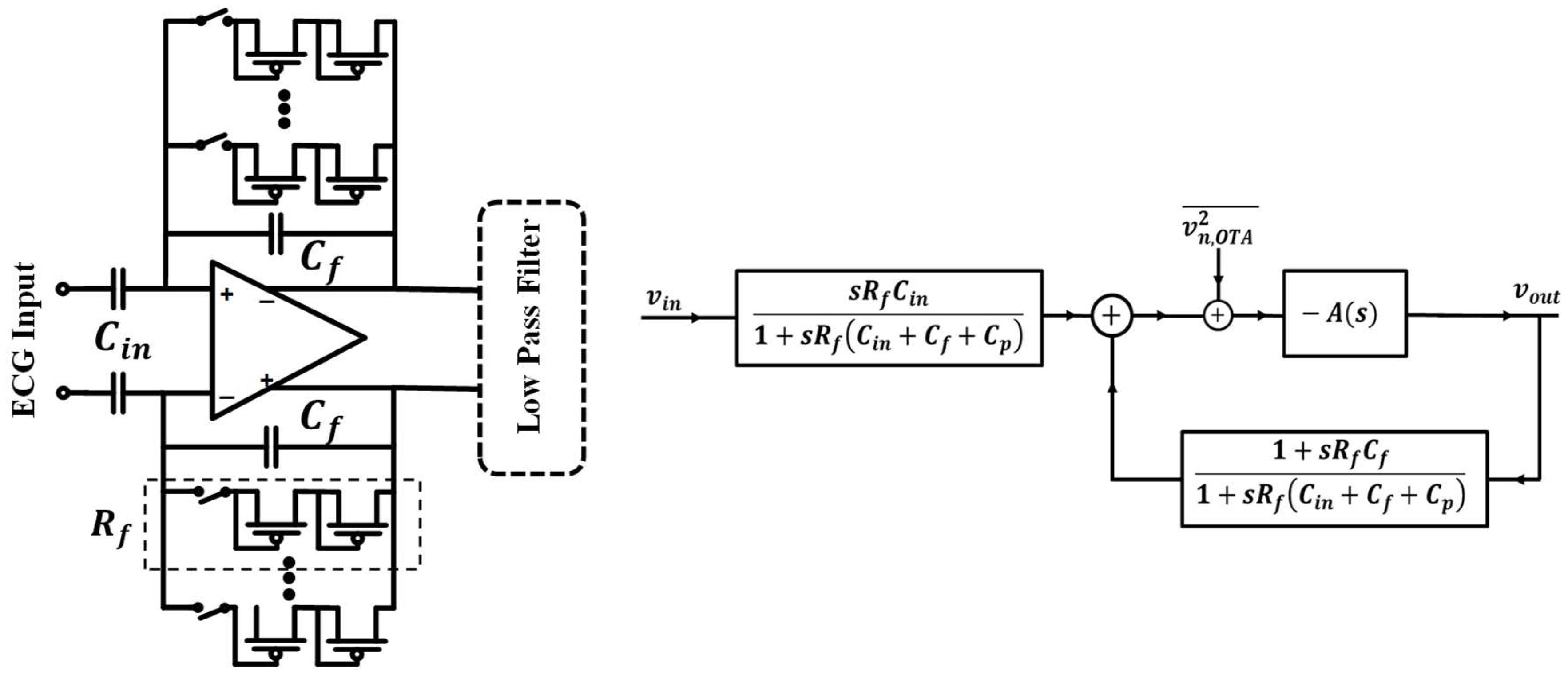
3.2.1. Capacitively Feedback Amplifier
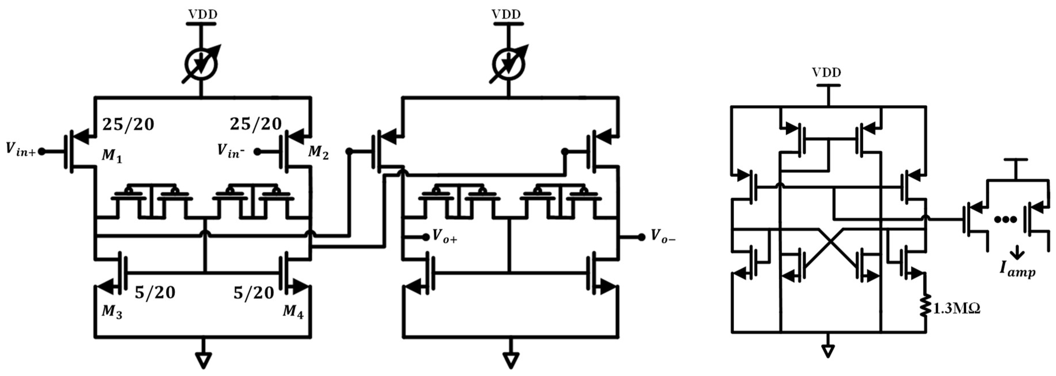
3.2.2. Design of the OTA
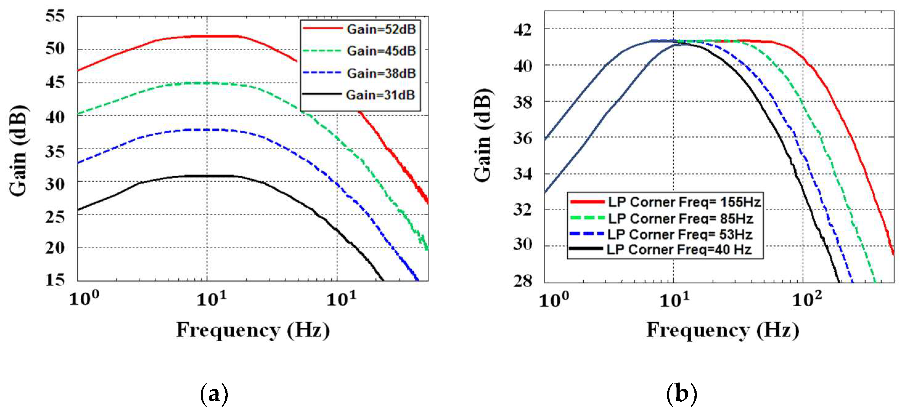
4. Low-Pass Filter and VGA Design
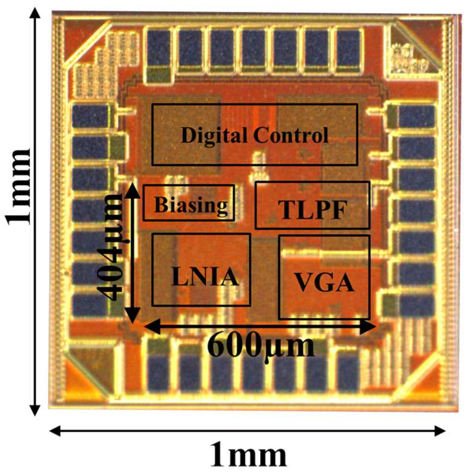
5. Experimental Results
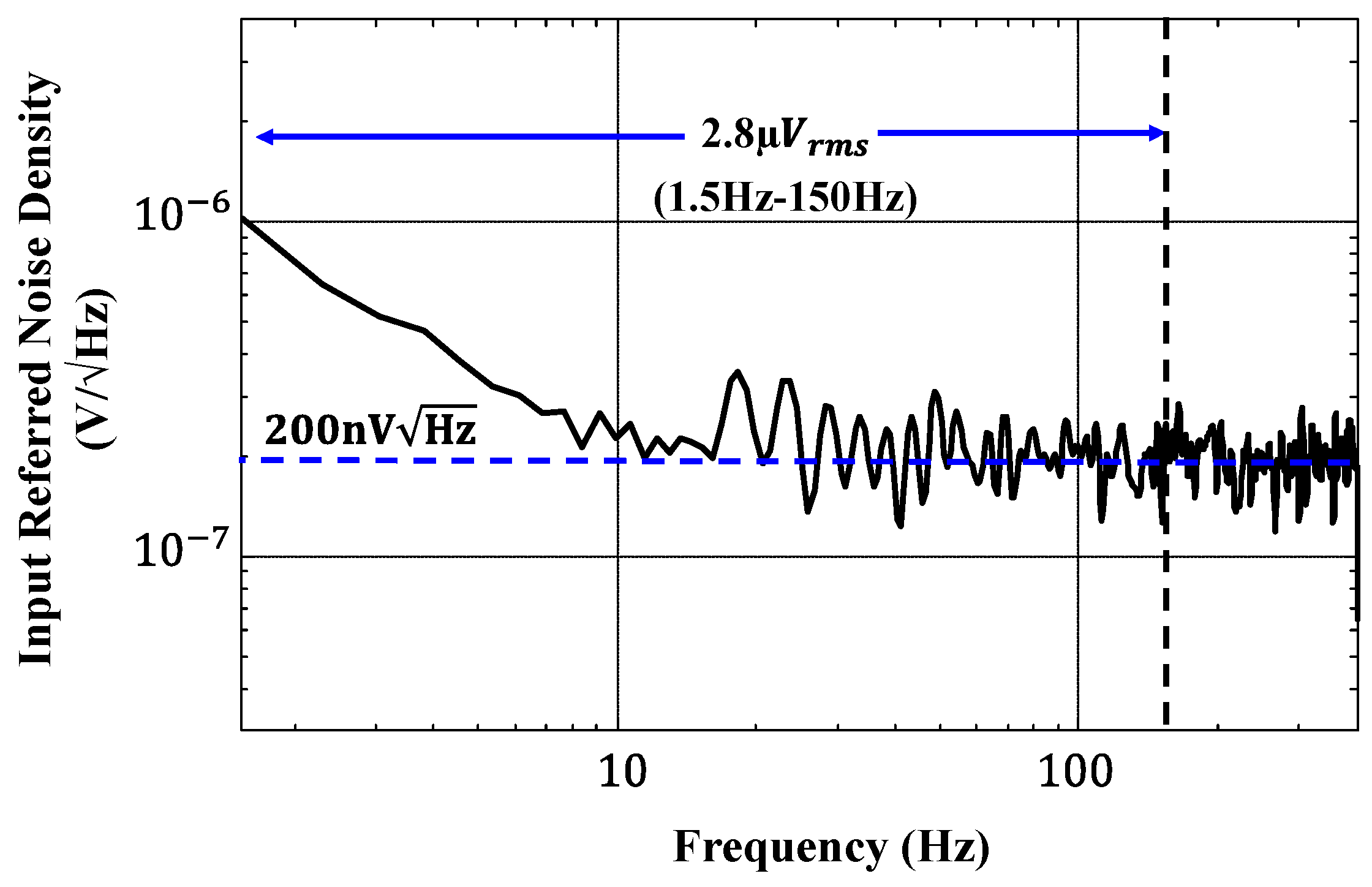
5.1. AFE Performance Measurements
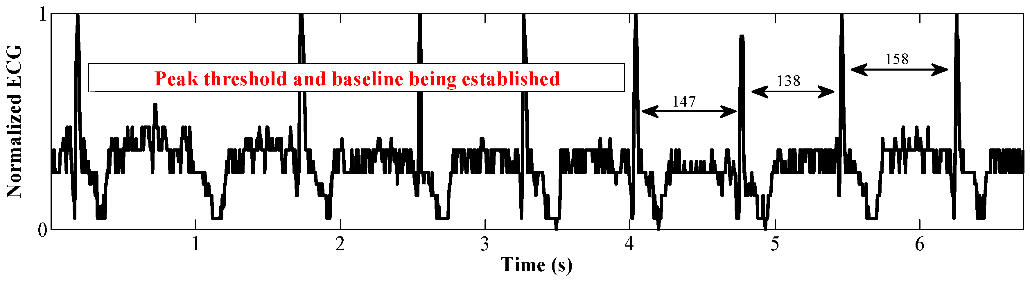
5.2. Arrhythmia Diagnosis
6. Conclusions
Author Contributions
Funding
Conflicts of Interest
References
- Zhang, Y.; Zhang, F.; Shakhsheer, Y.; Silver, J.D.; Klinefelter, A.; Nagaraju, M.; Boley, J.; Pandey, J.; Shrivastava, A.; Carlson, E.J.; et al. A Batteryless 19μW MICS/ISM-Band Energy Harvesting Body Sensor Node SoC for ExG Applications. IEEE J. Solid-State Circuits 2013, 48, 199–213. [Google Scholar] [CrossRef]
- Yahya, F.; Lukas, C.J.; Breiholz, J.; Roy, A.; Patel, H.N.; Liu, N.; Chen, X.; Kosari, A.; Li, S.; Akella, D.; et al. A Battery-less 507nW SoC with Integrated Platform Power Manager and SiP Interfaces. In Proceedings of the 2017 Symposium on VLSI Circuits, Kyoto, Japan, 5–8 June 2017. [Google Scholar]
- Kim, H.; Yazicioglu, R.F.; Kim, S.; van Helleputte, N.; Artes, A.; Konijnenburg, M.; Huisken, J.; Penders, J.; van Hoof, C. A configurable and low-power mixed signal soc for portable ECG monitoring applications. In Proceedings of the 2011 Symposium VLSI Circuits Digest of Technical Papers, Honolulu, HI, USA, 15–17 June 2011; pp. 142–143. [Google Scholar]
- Klinefelter, A.; Roberts, N.E.; Shakhsheer, Y.; Gonzalez, P.; Shrivastava, A.; Roy, A.; Craig, K.; Faisal, M.; Boley, J.; Oh, S.; et al. 21.3 A 6.45μW self-powered IoT SoC with integrated energy-harvesting power management and ULP asymmetric radios. In Proceedings of the 2015 IEEE International Solid-State Circuits Conference—(ISSCC) Digest of Technical Papers, San Francisco, CA, USA, 22–26 February 2015; pp. 1–3. [Google Scholar]
- Wahbah, M.; Alhawari, M.; Mohammad, B.; Saleh, H.; Ismail, M. Characterization of Human Body-Based Thermal and Vibration Energy Harvesting for Wearable Devices. IEEE J. Emerg. Sel. Top. Circuits Syst. 2014, 4, 354–363. [Google Scholar] [CrossRef]
- Muller, R.; Gambini, S.; Rabaey, J.M. A 0.013mm2 5μW DC-coupled neural signal acquisition IC with 0.5V supply. IEEE J. Solid-State Circuits 2012, 47, 232–243. [Google Scholar] [CrossRef]
- Chen, Y.-P.; Blaauw, D.; Sylvester, D. A 266nW multi-chopper amplifier with 1.38 noise efficiency factor for neural signal recording. In Proceedings of the 2014 Symposium on VLSI Circuits Digest of Technical Papers, Honolulu, HI, USA, 10–13 June 2014; pp. 1–2. [Google Scholar]
- Yoo, J.; Yan, L.; El-Damak, D.; Altaf, M.A.B.; Shoeb, A.H.; Chandrakasan, A.P. An 8-Channel Scalable EEG Acquisition SoC with Patient-Specific Seizure Classification and Recording Processor. IEEE J. Solid-State Circuits 2013, 48, 214–228. [Google Scholar] [CrossRef]
- Chandrakumar, H.; Markovic, D. A 2.8µW 80mVpp-linear-input-range 1.6GΩ-input impedance bio-signal chopper amplifier tolerant to common-mode interference up to 650mVpp. In Proceedings of the 2017 IEEE International Solid-State Circuits Conference (ISSCC), San Francisco, CA, USA, 5–9 February 2017. [Google Scholar]
- Yang, T.; Lu, J.; Jahan, M.S.; Griffin, K.; Langford, J.; Holleman, J. A configurable 5.9 μW analog front-end for biosignal acquisition. In Proceedings of the 2015 IEEE Custom Integrated Circuits Conference (CICC), San Jose, CA, USA, 28–30 September 2015; pp. 1–4. [Google Scholar]
- Jeon, D.; Chen, Y.P.; Lee, Y.; Kim, Y.; Foo, Z.; Kruger, G.; Oral, H.; Berenfeld, O.; Zhang, Z.; Blaauw, D.; et al. 24.3 An implantable 64nW ECG-monitoring mixed-signal SoC for arrhythmia diagnosis. In Proceedings of the 2014 IEEE International Solid-State Circuits Conference Digest of Technical Papers (ISSCC), San Francisco, CA, USA, 9–13 February 2014; pp. 416–417. [Google Scholar]
- Harpe, P.; Gao, H.; van Dommele, R.; Cantatore, E.; van Roermund, A. A 3nW signal-acquisition IC integrating an amplifier with 2.1 NEF and a 1.5fJ/conv-step ADC. In Proceedings of the 2015 IEEE International Solid-State Circuits Conference—(ISSCC) Digest of Technical Papers, San Francisco, CA, USA, 22–26 February 2015; pp. 1–3. [Google Scholar]
- Han, D.; Zheng, Y.; Rajkumar, R.; Dawe, G.; Je, M. A 0.45V 100-channel neural-recording IC with sub-µW/channel consumption in 0.18µm CMOS. In Proceedings of the 2013 IEEE International Solid-State Circuits Conference Digest of Technical Papers, San Francisco, CA, USA, 17–21 February 2013; pp. 290–291. [Google Scholar]
- Bohorquez, J.L.; Yip, M.; Chandrakasan, A.P.; Dawson, J.L. A Biomedical Sensor Interface with a sinc Filter and Interference Cancellation. IEEE J. Solid-State Circuits 2011, 46, 746–756. [Google Scholar] [CrossRef]
- Xiao, Z.; Tang, C.M.; Dougherty, C.M.; Bashirullah, R. A 20µW neural recording tag with supply-current-modulated AFE in 0.13µm CMOS. In Proceedings of the 2010 IEEE International Solid-State Circuits Conference—(ISSCC), San Francisco, CA, USA, 7–11 February 2010; pp. 122–123. [Google Scholar]
- Yazicioglu, R.F.; Kim, S.; Torfs, T.; Kim, H.; van Hoof, C. A 30 µW Analog Signal Processor ASIC for Portable Biopotential Signal Monitoring. IEEE J. Solid-State Circuits 2011, 46, 209–223. [Google Scholar] [CrossRef]
- Hsu, S.Y.; Ho, Y.; Tseng, Y.; Lin, T.Y.; Chang, P.Y.; Lee, J.W.; Hsiao, J.H.; Chuang, S.M.; Yang, T.Z.; Liu, P.C.; et al. A sub-100µW multi-functional cardiac signal processor for mobile healthcare applications. In Proceedings of the 2012 Symposium on VLSI Circuits (VLSIC), Honolulu, HI, USA, 13–15 June 2012; pp. 156–157. [Google Scholar]
- Wang, T.Y.; Lai, M.R.; Twigg, C.M.; Peng, S.Y. A Fully Reconfigurable Low-Noise Biopotential Sensing Amplifier with 1.96 Noise Efficiency Factor. IEEE Trans. Biomed. Circuits Syst. 2014, 8, 411–422. [Google Scholar] [CrossRef] [PubMed]
- Johnson, B.; Molnar, A. An orthogonal current-reuse amplifier for multi-channel sensing. IEEE J. Solid-State Circuits 2013, 48, 1487–1496. [Google Scholar] [CrossRef]
- Harrison, R.R.; Charles, C. A low-power low-noise CMOS amplifier for neural recording applications. IEEE J. Solid-State Circuits 2003, 38, 958–965. [Google Scholar] [CrossRef]
- Maruyama, M.; Taguchi, S.; Yamanoue, M.; Iizuka, K. An Analog Front-End for a Multifunction Sensor Employing a Weak-Inversion Biasing Technique with 26 nVrms, 25 aCrms, and 19 fArms Input-Referred Noise. IEEE J. Solid-State Circuits 2016, 51, 2252–2261. [Google Scholar] [CrossRef]
- Kligfield, P.; Gettes, L.S.; Bailey, J.J.; Childers, R.; Deal, B.J.; Hancock, E.W.; van Herpen, G.; Kors, J.A.; Macfarlane, P.; Mirvis, D.M.; et al. Standardization and Interpretation of the ECG, Part I, AHA/ACC/HRS Scientific Statement. Circulation 2007, 115, 1306–1324. [Google Scholar] [PubMed]
- Pan, J.; Tompkins, W.J. A real-time QRS detection algorithm. IEEE Trans. Biomed. Eng. 1985, BME-32, 230–236. [Google Scholar] [CrossRef] [PubMed]


| This Work | [6] | [7] | [8] | [10] | [18] | |
|---|---|---|---|---|---|---|
| Technology (nm) | 130 | 65 | 180 | 180 | 130 | 350 |
| VDD (V) | 0.5 | 0.5 | 1 | 1.8 | 1.2 | 2.5 |
| Area (mm2) | 0.24 | 0.013 | 0.25 | - | 0.4 | 0.17 |
| Blocks in comparison | AFE | AFE, ADC | AFE | AFE | AFE | AFE |
| Power (nW) | 68 | 5040 | 266 | 8250 * | 5300 | 82.5 |
| Gain (dB) | 31–52 | 32 | 42–51 | 52–80 | 45–71 | 40.7 |
| HP corner Freq. (Hz) | 0.5 | 1 | 1 | 0.07 | 1 | 0.05 |
| LP corner Freq. (Hz) | 40–250 | 300–10,000 | 500 | 30–100 | 100 | 100 |
| Input Referred Noise (µVrm) | 2.8 [1.5–155 Hz] | 4.9 [300 Hz–10 kHz] | 1.54 [1–500 Hz] | 0.91 [0.5–100 Hz] | 0.45 [1–100 Hz] | 2.8 [0.05–100 Hz] |
| Input Impedance (MΩ) | 115 | N/A | N/A | >500 | >100 | N/A |
| NEF | 2.78 | 5.99 | 1.38 | 5.12 | 3.7 | 1.96 |
| PEF | 3.9 | 17.96 | 1.9 | 47* | 16.4 | 9.6 |
| CMRR (dB) | 62 | 75 | 89 | >90 | >95 | >70 |
© 2018 by the authors. Licensee MDPI, Basel, Switzerland. This article is an open access article distributed under the terms and conditions of the Creative Commons Attribution (CC BY) license (http://creativecommons.org/licenses/by/4.0/).
Share and Cite
Kosari, A.; Breiholz, J.; Liu, N.; Calhoun, B.H.; Wentzloff, D.D. A 0.5 V 68 nW ECG Monitoring Analog Front-End for Arrhythmia Diagnosis. J. Low Power Electron. Appl. 2018, 8, 27. https://doi.org/10.3390/jlpea8030027
Kosari A, Breiholz J, Liu N, Calhoun BH, Wentzloff DD. A 0.5 V 68 nW ECG Monitoring Analog Front-End for Arrhythmia Diagnosis. Journal of Low Power Electronics and Applications. 2018; 8(3):27. https://doi.org/10.3390/jlpea8030027
Chicago/Turabian StyleKosari, Avish, Jacob Breiholz, NingXi Liu, Benton H. Calhoun, and David D. Wentzloff. 2018. "A 0.5 V 68 nW ECG Monitoring Analog Front-End for Arrhythmia Diagnosis" Journal of Low Power Electronics and Applications 8, no. 3: 27. https://doi.org/10.3390/jlpea8030027
APA StyleKosari, A., Breiholz, J., Liu, N., Calhoun, B. H., & Wentzloff, D. D. (2018). A 0.5 V 68 nW ECG Monitoring Analog Front-End for Arrhythmia Diagnosis. Journal of Low Power Electronics and Applications, 8(3), 27. https://doi.org/10.3390/jlpea8030027