Article

A Survey of Low Voltage and Low Power Amplifier Topologies

Department of Information Engineering, University of Brescia, 25121 Brescia BS, Italy
*
Author to whom correspondence should be addressed.
J. Low Power Electron. Appl. 2018, 8(3), 22; https://doi.org/10.3390/jlpea8030022
Submission received: 3 May 2018 / Revised: 11 June 2018 / Accepted: 20 June 2018 / Published: 23 June 2018
(This article belongs to the Special Issue CMOS Low Power Design)

Abstract

:
Reducing voltage supply is one of the most effective way to reduce the power consumption, but, on the other hand it is a challenging choice for the analog designers. In this paper, different topologies, well-suited for low voltage and ultra-low voltage supply, are depicted, investigated, designed in the same standard 180 nm technology and compared, highlighting the benefits and the possible applications.

1. Introduction

One of the most effective ways to save the power is to reduce the voltage supply. On the other hand, low voltage and ultra low voltage design is challenging, especially for analog circuits. Among them, the operational trasconductance amplifier (OTA) represents the most common and used block and thus a lot of work has been and is currently devoted to fullfil the requirements of DC gain, bandwidth and slew rate, which are limited by the low voltage condition. For example, indeed, cascoding is not allowed because of the voltage headroom. Therefore, analog designers are using novel architectures, such as, for example, inverter-based amplifiers [1,2,3,4,5], bulk-driven and self-cascode topology [6,7], hybrid-mode input stage [8] and rail-to-rail amplifier with cross-coupled output stage [9]. In this paper, these novel topologies are analyzed, and compared, using the same standard 180 nm CMOS technology. Moreover, a nMOS-only amplifier architecture [10] has been verified in the context of low voltage supply. The paper is organized as follows: in the second section the amplifier architectures will be depicted; in the third section they will be simulated and compared, highlighting the advantages and the possible applications; in the fourth section conclusions will be drawn.

2. Amplifier Topologies

In this section, recent architectures of CMOS amplifiers are depicted. The schematics are also sized and simulated using the Design Kit of the CMOS technology UMC (United Microelectronics Corporation) 180 nm.

2.1. Inverter Based Amplifier

The technology scaling favors digital circuits, by improving speed and reducing dynamic power dissipation. Moreover, the voltage supply is constantly reduced, making the analog design challenging. In this context, is rising the trend of implementing low-voltage, inverter-based analog circuits. Among them, examples of inverter-based OTAs can be found recently [1,2,3,4,5]. In this subsection, we consider three different designs: the first one is a single stage inverter-based fully differential amplifer [1], while the second one is a three stage inverter-based amplifier with a feed-forward compensation technique [2] and the last one is a current-starved amplifier [5].

2.1.1. Tunable Inverter-Based Amplifier

The inverter-based amplifier has the same topology of the CMOS digital inverter, but operates at a common-mode (CM) voltage keeping both the nMOS and pMOS transistors in the saturation region. This results in high transconductance and output resistance, and consequently high dc gain and gain bandwidth (GBW). The gain of the inverter stage can be indeed written as:
A v = g m n + g m p g d s n + g d s p
where g m is the transconductance and g d s is the inverse of the small signal output resistance. However, a main disadvantage of operating the inverter as an amplifier is the high variation of the inverter dc gain and gain bandwidth (GBW), with temperature and process corners. To overcome this problem, a simple circuit technique can be used to tune inverter-based amplifiers across the process and temperature variations. The conceptual schematic of the inverter-based amplifier is shown in Figure 1, while the detailed description is given in [1].
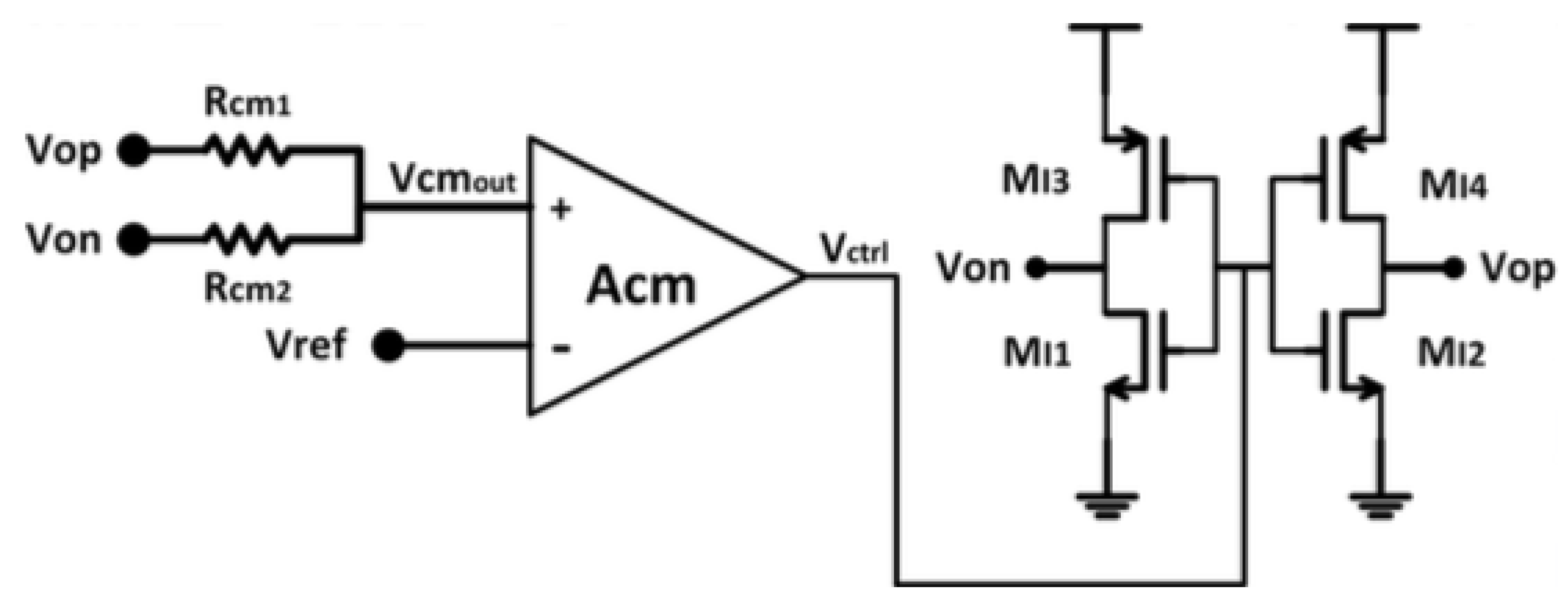
The tuning technique is basically a CM feedback (CMFB) circuit that senses the output CM voltage and controls the current flow through the inverter using four controlled current sources. Indeed, the small signal parameter gm and gds are highly dependent on the voltage drop between the drain and source Vds which, in the inverter topology, is also the common mode (CM) output voltage. Therefore, for a simple inverter-based OTA, fixing the output CM helps, also, to fix the dc gain, and the dc-gain variation becomes limited to the variation in the threshold voltage. The tuning circuit maintains a robust operation with small dc-gain variations across the temperature and process corners, by fixing Vds of both the nMOS and pMOS transistors, for the OTA. Figure 2 shows the implementation of the tuning circuit. Stacking a tunable current source within the main OTA would consume voltage headroom, therefore the current sources that receive the control signal from the CMFB amplifier (Acm) are added in parallel to the OTA output transistors. The CM of the OTA is extracted using two resistors and compared with a reference voltage (Vref), set at the half the supply voltage, using the amplifier Acm, shown in Figure 3. The output of the amplifier controls the nMOS and pMOS current sources (MI1–MI4). The CMFB current sources can source or sink current into the main OTA. The Acm amplifier is a simple pseudodifferential amplifier. At a certain temperature and process corner, if the output CM voltage (Vcmout) is lower than Vref, then Vctrl becomes low. This forces MI3 and MI4 transistors to source more current into the main OTA until Vcmout nearly equals Vref. The opposite operation happens when Vcmout is higher than Vref.
The proposed circuit maintains the output CM of the inverter-based amplifier, without requiring any additional voltage headroom to the simple inverter structure. Therefore, the low-voltage operation is achieved.

2.1.2. Inverter-Based Amplifier with Feed-Forward Compensation

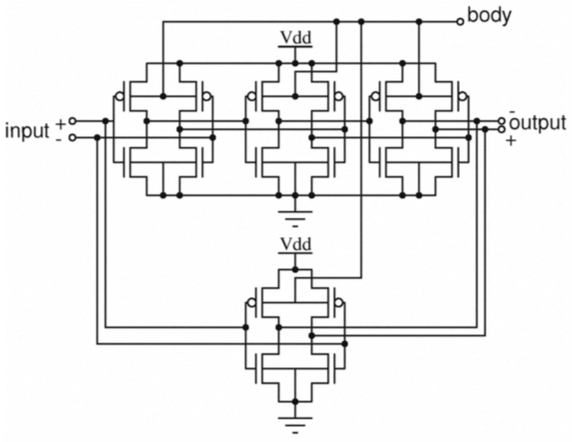
In [2] a different inverter-based amplifier is proposed and widely discussed. It is based on the cascade of three stages with feed-forward compensation, to achieve a reasonable gain without sacrificing the bandwidth. The conceptual schematic is shown in Figure 4 and the detailed schematic is drawn in Figure 5: at low frequency, the three stage amplifier provides a gain of approximately ( A O ) 3 , while at high frequencies, since path B is faster, the amplifier shown only the gain of the single stage in the feedback loop ( A F ) . For the sake of completeness, the low frequency gain is given by:
A O 3 = ( g m · r d s ) · α + g m 2 r d s 2 1 + α
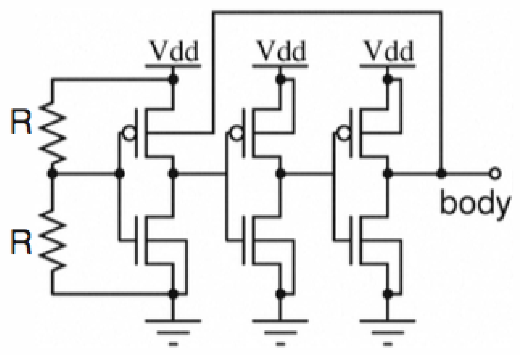
where g m is the sum of the transconductances of the nMOS and pMOS devices, r d s is the parallel combination of the output resistances of the nMOS and pMOS devices, and α is the ratio between the geometry of the transistors in the path B and the corresponding in the path A. As already stated, the main drawback of the inverter used as an amplifier is the high variation of its AC characteristics (dc gain and gain bandwidth (GBW)), with temperature and process corners. Therefore, a biasing circuit is added (and shown in Figure 6) which bias the n-well of the pMOS transistors, so to allow high gain at a fixed middle supply CM voltage, independently of process, temperature and power supply variations. The ratio between the transistors of path A and path B is chosen to achieve the desired phase margin.

2.1.3. Current-Starved Inverter-Based Amplifier

As already stated, an interesting solution in designing amplifier working with very low voltage supply is the inverter-based topology. When the inverter-based amplifier is implemented at a low supply voltage, the transistors will operate in the sub-threshold region, with a consequent reduction of bias currents and power consumption and, at the same time, of bandwidth and amplifier driving capability. A modification of the standard inverter-based amplifier is proposed in [5]: the novel input stage includes a couple of tail current sources (both N and P type) to better control the current through the inverters, pushing the transistors further into the sub-threshold region, and further reducing power consumption. The tail sources can also improve the amplifier’s CMRR (Common-mode rejection ratio) and provide an additional input that can be used for common-mode feedback, overcoming the problems of the original inverter-based design. In addition, the use of tail separates the need for low power consumption and low input offset voltage: the inverters can be sized, indeed, appropriately to control offset voltage while the tail controls the overall power consumption.
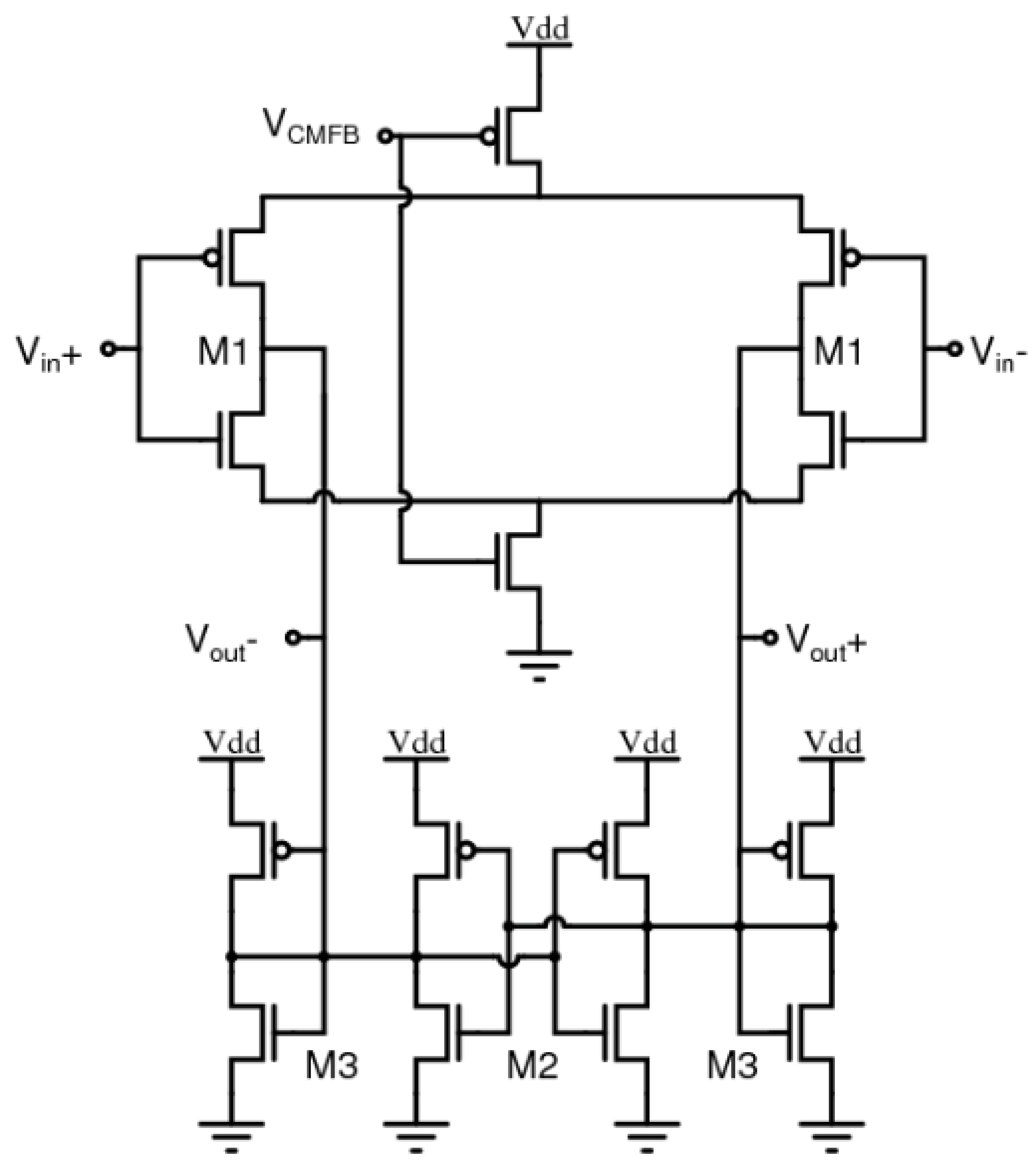
The proposed topology shown in Figure 7 employs an active load consisting of four additional load inverters (M2, M3). M2 is connected in a cross-coupled configuration, while the outer pair of inverters (M3) is diode-connected as shown in Figure 7. The cross-coupled pair provides positive feedback and therefore a negative resistance of −2/ g m 3 . The diode connected pair provides a positive resistance of 2/ g m 2 . This positive resistance helps stabilize the unstable negative impedance of the cross-coupling, as well as providing DC bias stability for both the input and cross-coupled inverter pairs. This combination of positive and negative impedances gives the active load circuit a large output impedance equal to the inverse of ( g m 2 g m 3 ). The overall voltage gain of the amplifier’s half-circuit can then be defined as:
A v = g m 1 g m 2 g m 3
When sizing the transistors in this design, it is desirable for the input and tail transistors to have reasonably large lengths (typically more than 1 μ m) and large W/L ratios (typically more than 16) to improve output impedance, and to have an increased transconductance.

2.2. Bulk-driven Ampliifer

A bulk-driven Miller amplifier is composed of an input differential pair, a current source, an active load and a common source stage. The gain of the input stage is given by the small signal parameter gmb (bulk transconductance), which is of course much lower than gm (gate transconductance), multiplied by the output resistance; this results in a smaller gain and gain-bandwidth product of the bulk-driven topology respect to the classical gate-driven. However, compared to the standard gate-driven Miller OpAmp, in the bulk-driven one the input signals arise from the bulk of the differential pair, while the gate, the source and the drain voltages provide the bias of the transistors. This technique is especially appealing in the field of ultra low voltage applications, in particular biomedical, because the latter need a low power consumption and very low voltage supply, without requiring mostly a large gain-bandwidth product. Moreover, thanks to the bulk-driven technique, the input stage exhibits a better common mode input range, compared to the gate-driven topology. The bulk-driven amplifier exhibits also a lower susceptibility to the Electromagnetic Interferences, as depicted in [11]. Nevertheless, considering a P-type bulk-driven input stage, one can say that the circuit shows a poor linearity if the common-mode voltage is close to the negative rail. The differential pair causes, indeed, distortion to the signal, since the active load starts switching off. The analog happens for the N-type input stage if the common-mode voltage is close to the positive rail. To solve this problem, two batteries should be placed in series with the active load, to provide a dc shifting on the signal; in this way, the active load remains operational with constant voltage for lower values of the input signal, thus avoiding non linearity conditions. The battery can be replaced by a common-gate amplifier. In terms of dc analysis, indeed, the transistor in diode configuration can be modeled by a resistance whose value is given by the inverse its transconductance, emulating a battery. Nevertheless, in terms of ac analysis, the composite transistor Q3–Q4 is an active load, and it presents a gain. A modified bulk-driven Miller amplifier, based on composite folded active load, is therefore presented in [6]. The composite transistor is an important configuration for MOS transistor in weak inversion, and generally for low voltage applications, because it presents a better gain respect to the single transistor without consuming voltage headroom.
The overall gain of the amplifier in Figure 8 is that of a two stage amplifier. The second stage provides the typical gain of a common source stage with active load and it can be written as:
A v I I = g m 6 g d s 6 + g d s 7
The first stage has a gain similar to that of a folded cascode amplifier with a bulk driven input stage:
A v I = g m b 2 g d s 9 + g d s E Q
where g d s E Q is the output resistance of the cascode load (Q4a, Q4b, Q2), approximately given by:
g d s E Q = g m 4 + g m b 4 g d s 4 · 1 g d s 4 a + g d s 2
The frequency behaviour is very similar to that of a standard two-stage amplifier and therefore the Miller compensation is added to assure the stability. Moreover, to increase the DC-gain, the schematic proposed in [6] can be improved by adding a cross-coupled pair to the bulk-driven input OTAs, which provides the positive feedback, as depicted in [7]. The transconductance with the positive feedback becomes indeed much larger than the transconductance gmb in the conventional bulk-driven input. Moreover, the frequency response of the classical two-stage schematic is improved in [7] by using an indirect feedback compensation method which expands the bandwidth and reduces the compensation-capacitor at a sub-threshold voltage.

2.3. Hybrid Mode Amplifier

Voltage regulator is another fundamental analog building block, based on an error amplifier and a power transistor which drives the loads. In low voltage and low power applications, it presents the major challenge of achieving a good dynamic response with a low quiescent current. Therefore, the adaptive biasing scheme is used, because its the quiescent current is very small at low-load condition and gradually increases to a high value at high-load condition. Hence, when the load current switches from the high-to-low load condition, the higher quiescent current at high-load condition initially provides a fast charging of the gate node of the power transistor connected to the error amplifier, resulting in a small overshoot at the output. However, for the low-to-high load transient edge, the low quiescent current provides a larger undershoot due to the slow discharging of the gate node of the power transistor. For this purpose, a hybrid-mode operational transconductance amplifier (HM-OTA) has been proposed, that does not occupy extra space in silicon or consume additional power to realize, while presenting a fast discharging slew-rate and achieving a good dynamic response. The hydbrid-mode amplifier is depicted in [8] and it is shown in Figure 9c, where its topology is compared to the common-mode amplifier (CM-OTA) in (a) and to the differential-mode (DM-OTA) in (b).
The first one (Figure 9a) is the common-mode amplifer: it is a possible solution for implementing the error amplifier in the voltage regulator due to its single pole behavior, which eases frequency compensation. However, it has very limited dc gain as all the internal nodes have low impedance. Moreover, under large signal operation, the charging/discharging slew rate is also symmetric and quite limited. For the sake of completeness, the gain A v of the CM-OTA is approximately given by:
A v = g m 82 g m 84 · g m 87 g d s 87 + g d s 90 + g m 81 g m 83 · g m 88 g d s 87 + g d s 90
and it is similar to a one-stage amplifier. A conventional differential-mode OTA (DM-OTA) (Figure 9b) is a more preferred option, as it provides a high dc gain as well as asymmetric slewing operation in large signal. The gain A v is indeed:
A v = g m 82 g m 84 · g m 87 g d s 87 + g d s 90 + ( g m 81 g d s 81 + g d s 83 + g m 82 g m 84 · g m 83 g d s 81 + g d s 83 ) · g m 88 g d s 87 + g d s 90
and it is the two-stage amplifier gain. However, the high impedance from the internal node creates a stability issue in the regulator with a small value of output compensation capacitor and a low quiescent current. Essentially, the value of the output capacitor has to be increased to restore the stability. The HM-OTA is constructed by combining both the CM-OTA and the DM-OTA as shown in Figure 9c and exploits the advantages of both the structures. Unlike the CM-OTA, the transistor M 83 is segmented into two parts namely, M 83 a and M 83 b . Also, the gate of M 83 b is connected to V1 instead of the node V2 in the proposed HM-OTA. This modification forms a localized differential stage, which forces the delta/difference current of I 81 and I 83 b through I 83 a . The ratios of M 84 : M 83 b and M 83 a : M 83 b are chosen as 1: α and (1- α ): α , respectively, for maintaining dc current balancing in the HM-OTA. So, the HM-OTA becomes a combination of α xCM-OTA and (1− α )xDM-OTA for 0 α 1 . The differential gain is in this case:
A v = g m 82 g m 84 · g m 87 g d s 87 + g d s 90 + ( g m 82 g m 84 · g m 83 b g m 83 a + g m 81 g m 83 a ) · g m 88 g d s 87 + g d s 90
and it is the gain of an improved one-stage amplifier. The slew-rate performance of the proposed HM-OTA is discussed now. During large signal operation, the charging slew rate SR+ is similar to the conventional CM-OTA/DM-OTA. During discharging operation, the transistors M 82 , M 84 , M 83 b completely shut off and the whole tail current flows through M 81 and M 83 a . Due to the width ratio of M 83 a and M 88 the negative SR is higher than the conventional CM-OTA by a factor of 1/(1− α ). Of course, the value of SR- of HM-OTA is still less than the conventional DM-OTA; however the latter causes a stability issue in the regulator as mentioned before. The main advantage of the HM-OTA over the CM-OTA and the DM-OTA is that the dc gain, loop bandwidth, slew rates, and loop stability can be easily controlled with the value of α . Also, this modification does not require any additional space and quiescent current.

2.4. Rail-to-Rail Amplifier with Cross-Coupled Output Stage

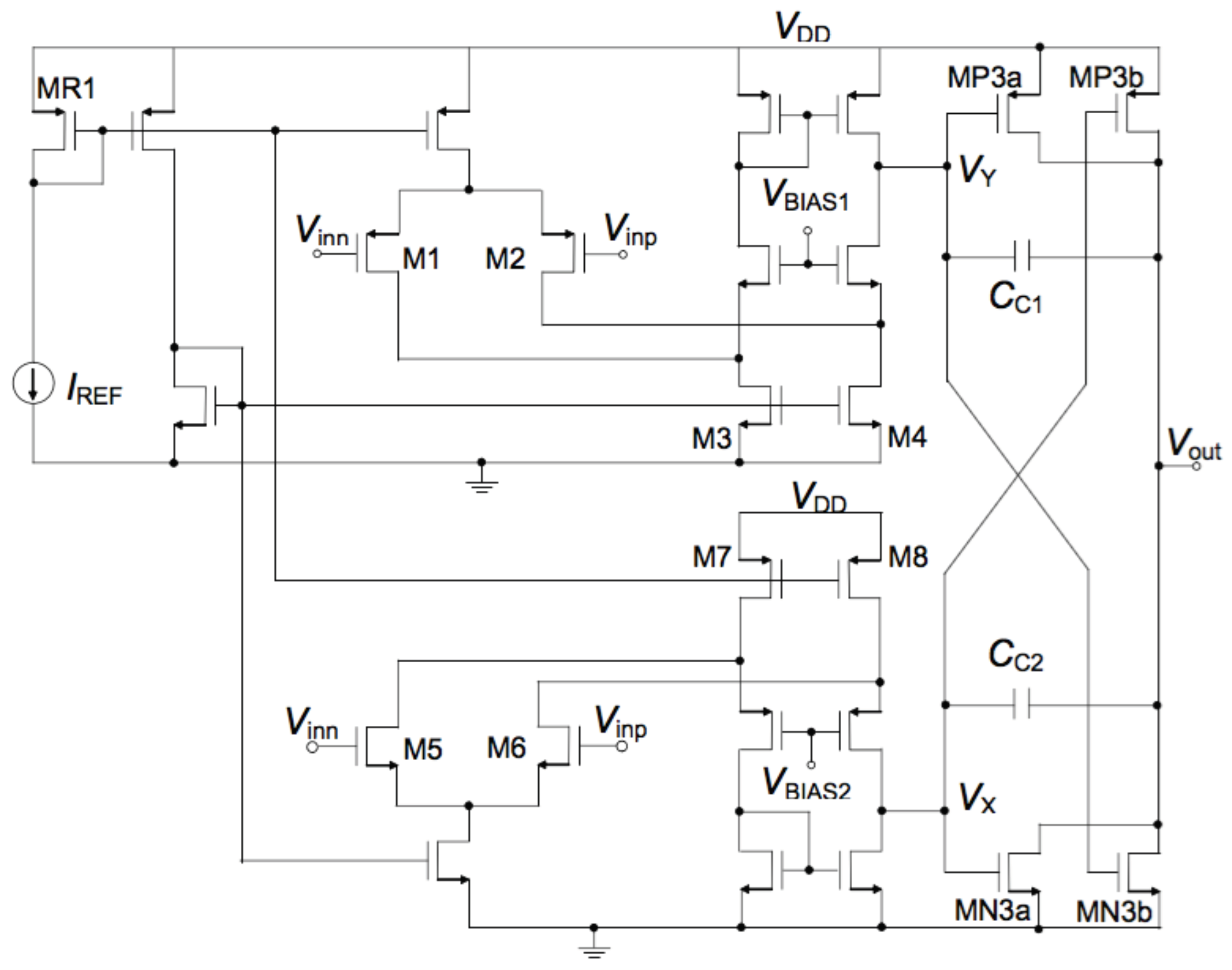
In Figure 10 rail-to-rail operational amplifier with ultra-low-power operation is shown. The amplifer has a two-stage architecture based on a complementary input stage and a novel cross-coupled output stage. The cross-coupled output stage increases the transconductances of the MOSFETs of the output stage without requiring additional chip area. Hence, it increases the gain of the amplifier and drivability for a capacitive load.
The voltage gain of the amplifier is given by A V I multiplied by A V I I , which are approximately:
A v I = g m 2 g d s C a s c o d e N + g d s P + g m 6 g d s C a s c o d e P + g d s N
A v I I = g m P 3 a + g m N 3 b g d s o u t + g m N 3 a + g m P 3 b g d s o u t
where g d s o u t is given by the conductance of the cross-coupled output stage and therefore, it is:
g d s o u t = g d s P 3 a + g d s P 3 b + g d s N 3 a + g d s N 3 b
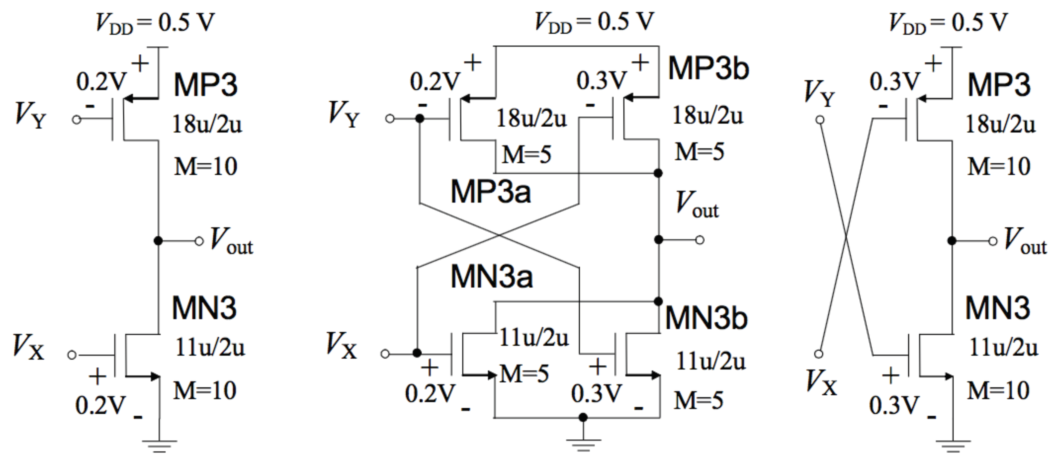
The architecture is well explained in [9] but the output stage is also reported in Figure 11 for the sake of clarity. In brief, the output stage proposed in [9] is divided in two branches, one cross-coupled and the other one in standard common-source topology. This exploits in increased transconductance and therefore enhanced gain and drivability for a capacitive load, respect to the standard common-source stage, with moderate current consumption, respect to the fully cross-coupled topology. The frequency behaviour is similar to that of a standard two-stage amplifier and therefore a Miller compensation capacitance is added between the output of the first and the second stages.

2.5. NMOS-Only Amplifier

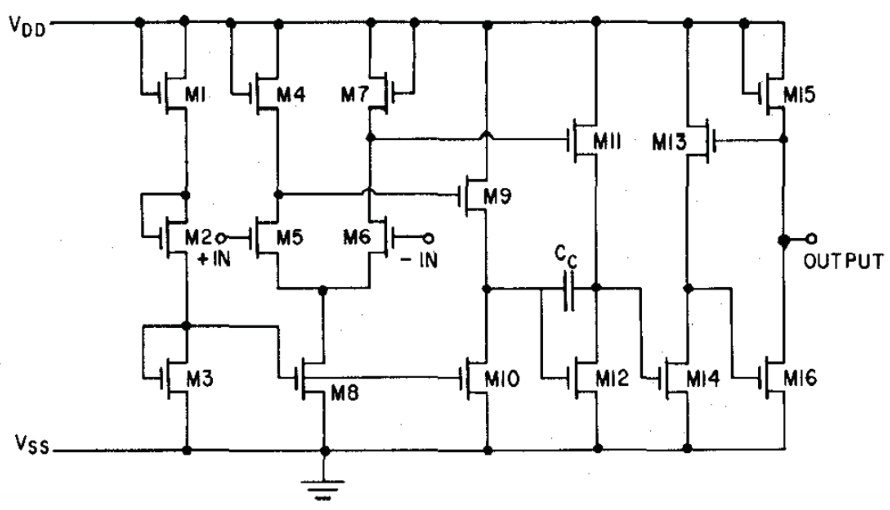
Another interesting architecture for low voltage and ultra low voltage applications is the one proposed in 1979 in the paper [10]. This amplifier is only based on nMOS devices, as shown in Figure 12; neverthless it provides the gain required in most of low voltage applications (such as, for example, biomedical and sensors). The nMOS-only amplifier is attractive because in recent technologies nMOS native transistors (i.e., with extremely low threshold voltage) are available and therefore an architecture based only on nMOS transistors allows for a very low voltage supply. Moreover, no cascode devices are needed and therefore the architecture can be strongly recommended to low voltage supply. Also, this amplifier topology can be interesting in the organic technologies where avoiding the use of complementary devices can be paramount [12]. The amplifier is based on a source coupled differential pair as input stage ( M 5 , M 6 , M 8 ) with diode-connected nMOS as active load ( M 4 , M 7 ); on two source follower level shifts ( M 9 , M 11 ), a second gain stage ( M 12 , M 11 ) and an output stage ( M 13 , M 14 , M 15 , M 16 ). The overall voltage gain can be approximately given by the product of the ratios between the transistors transconductances g m and can be written as:
A v = g m 5 g m 4 · g m 12 g m 11 · g m 14 g m 13 · g m 16 g m 15
it is worth noting that a compensation capacitance must be added C C between the main gain stages to assure the stability when the amplifier is in closed loop configuration.

3. Results and Comparison

All the above architectures have been sized and designed in the standard UMC 180 nm CMOS technology. The layout has been carefully designed and schematic equivalent to its extracted view has been simulated. The UMC 180 nm technology is widely used in analog design because it is a ripe technology with good design kit. It provides devices for medium and low voltage supply (namely 3.3 V and 1.8 V respectively), with regular and low threshold, triple-well nMOS (along with the bulk devices) and it also provides a zero threshold nMOS transistor. Six metal levels, high resistive poly and metal-metal capacitors are available in this technology. Along with the main AC characteristics, the classical amplifier FOM (Figure Of Merit) has been also evaluated. For the sake of clarity, FOM is defined as:
F O M = G B W · C L I V d d
where the G B W is the 0 dB frequency, C L is the load and I V d d is the overall biasing current.

3.1. Tunable Inverter-Based Amplifier

The tunable inverter-based amplifier is designed using the standard transistors of the UMC 180 nm technology, having a nominal threshold voltage of about 340 mV (for the N-type transistors) and 500 mV (for the P-type). The circuit is therefore supplied by a voltage Vdd of 1 V. For the sake of completeness, the proposed amplifier inlcuding the CMFB circuit is compared to a simple inverter-based fully-differential stage. In the latter, the pMOS transistors are sized of 350 μ m for the width and 2 μ m for the lenght, while the nMOS are of W = 100 μ m and L = 2 μ m.The transistors sizing of the inverter-based amplifier with CMFB is, instead, listed in Table 1.
The simple inverter-based amplifier and the amplifier with CMFB are both simulated and compared, showing very similar nominal AC characteristics which are here listed: gain of 45 dB, cut-off frequency of about 1.5 MHz, GBW of 200 MHz, phase margin of 80 . Both the amplifiers have a similar power consumption: 129 μ W for the simple amplifier and 134.5 μ W for the amplifier with CMFB. The amplifier with CMFB circuit exhibits a larger common mode range (about 100 mV instead of the very narrow range—9 mV—of the simple inverter-based amplifier) and a better behavior when considering the process and temperature variation. For example, by considering the corner analysis, the gain of the amplifier wth CMFB is always above 40 dB, while the simple amplifier does not work in one corner condition, and a similar result occurs also if the temperature is varied in the range between −40 C and +80 C. Therefore we can say that the tunable inverter-based amplifier is a more robust circuit compared to the simple one. The final layout of the inverter-based amplifier with CMFB occupies an area of about 120 μ m × 40 μ m and the calculated FOM is of 1.6.

3.2. Inverter-Based Amplifier with Feed-Forward Compensation

To investigate the feasibility of the inverter-based amplifier with feed-forward compensation, it has been first designed for 1.2 V voltage supply, but its performances have been also evaluated for lower and lower Vdd (down to 0.4 V). For the three inverter stage of the path A, the length has been chosen of 240 nm, the pMOS width of 18 μ m and the nMOS width of 6 μ m. For the inverter stage of the path B, the length is 240 nm, the pMOS width is 270 μ m and the nMOS width is 90 μ m. For the bulk voltage reference circuit, R is 10 k Ω , the length of all the transistors is again 240 nm, the pMOS width is 24 μ m, the nMOS width is 6 μ m.
The layout of the overall circuit occupies an area of about 60 μ m × 40 μ m.
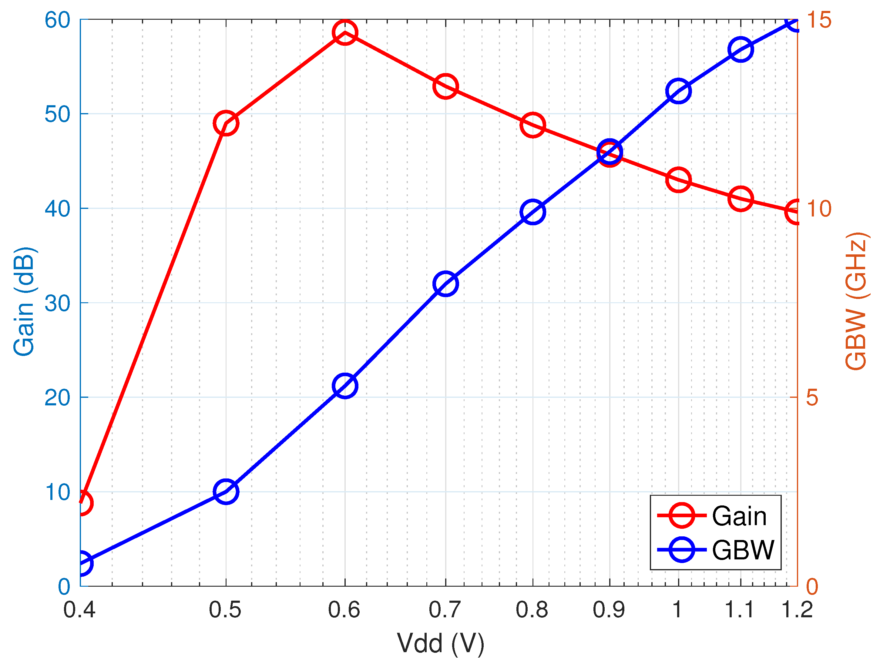
The simulations have been performed on the circuit equivalent to the extracted layout, at different Vdd conditions, ranging from 0.4 V up to 1.2 V; the common mode has been kept at Vdd/2. Gain, gain-bandwidth product and phase margin (PM) have been listed in Table 2. For a better readability the gain and the gain-bandwidth are also plotted versus the voltage supply in Figure 13.
As highlighted by the table, the amplifier is well suited also for ultra low voltage supply; moreover, it is worth noting that these simulations at different voltage supplies have been performed on the original amplifier design (i.e., the one optimized for 1.2 V) without any sizing arrangement or changes. FOM has been evaluated on 1.2 V of Vdd and it is of 4.24. Finally, corner analysis was performed in the nominal Vdd condition: the gain changes only of 4 dB and the GBW is always above 10 GHz with a good phase margin. Due to the medium gain and the very large bandwidth, this amplifier can be used for high data-rate applications which require low voltage (for example in biomedical image recording and processing).

3.3. Current-Starved Inverter-Based Amplifier

The current-starved inverter-based amplifier has been designed in the UMC 180 nm technology. The nominal voltage supply has been chosen of 1.1 V and the required driving capability at 1.1 V Vdd is refered to a capacitive load of 15 pF. Good voltage gain, bandwidth, stability and rejection of common-mode signals are required as well. In addition, the power consumption must be kept below a few tens of μ W. The transistors’ sizing are listed in Table 3.
The layout of the circuit occupies an area of about 40 μ m × 40 μ m. It was extracted and the resulting amplifier was simulated: it presents a gain of 53 dB, a GBW of 3.6 MHz with a phase margin of 90 , a CMRR of 233 dB and a power consumption of 21 μ W.
The same amplifier (with the same transistors’ sizing) was also simulated at different biasing conditions, and in particular with a voltage supply of 0.9 V and 0.7 V, in order to investigate its behavior in the case of ultra-low voltage applications. The main characteristics of the amplifier at different voltage supply are, therefore, reported in Table 4. The behavior of this amplifier is satisfactory also at very low voltage supply, as shown in the table. Moreover, the figure of merit (FOM) depends on the value of Vdd and it is of 1.93 for 0.7 V Vdd, of 3.45 for 0.9 V Vdd, of 2.87 for 1.1 V Vdd.

3.4. Bulk-Driven Amplifier

The bulk-driven amplifier proposed in [6], has been sized for the UMC 180 nm CMOS technology, with these requirements: a voltage supply of 0.5 V, gain of 30 dB at least, GBW of 100 kHz with 10 pF capacitive load. The amplifier dimensions are listed in Table 5 and refer to Figure 6.
Moreover, the biasing current has been chosen of 140 nA; C C is 1pF and R C is not mandatory for the phase margin. The final layout occupies an area of 50 μ m × 20 μ m, it has been extracted and the equivalent circuit was simulated. The main characteristics of the amplifier are here summarized. The gain is of 36 dB; the GBW and the phase margin for a load of 10 pF are, respectively, 277 kHz and 70 . The amplifier has a power consumption of 554 nW and a good rejection of both common-mode and power-supply noise: the common-mode rejection ratio (CMRR) is indeed 75 dB and the positive and negative power supply rejection ratio (PSRR) are around 80 dB. Moreover, the FOM is of 1.03. Therefore, this amplifier is well suited for biomedical applications where the physiological signals can be processed at low-medium frequency and where the power consumption must be reduced while keeping a high rejection of common mode signals and noise.

3.5. Hybrid-Mode Amplifier

The hybrid-mode amplifier proposed in [8] has been sized for the UMC 180 nm CMOS technology with a nominal voltage supply of 1.8 V. The layout was designed considering matching issues and it has been extracted and simulated. The extracted equivalent circuit presents a gain of 45 dB, a GBW of 20 MHz and a phase margin of 50 when it drives a capacitive load of 5 pF. The parameter α has been chosen of 0.5. Therefore the slew rate is almost doubled respect to the CM amplifier and the frequency behavior is better than the DM one. Moreover, thanks to the traditional input stage, which is a classical differential pair, the common mode input range is nearly rail-to-rail. The amplifier dimensions are listed in Table 6 and refer to Figure 9.
The final layout occupies an area of 60 μ m × 40 μ m and the FOM is 1.21.

3.6. Rail-To-Rail Amplifier with Cross-Coupled Output Stage

The rail-to-rail amplifier with the cross-coupled output stage has been sized for the technology UMC 180 nm. The design constraints are the voltage supply of 0.5 V and the capacitive load of 40 pF. The voltage gain must be higher than 70 dB and a gainbandwidth product of 10 kHz is required; at the same time, the power consumption must be reduced below the μ W. All the transistors work in the weak inversion region with an overdrive voltage of about 100 mV; their dimensions are listed in Table 7 and refer to Figure 10.
The layout, carefully designed considering the matching issues, occupies an area of 160 μ m × 40 μ m; it has been extracted and the equivalent circuit was simulated. Corner analysis was also performed because the Montecarlo models are not available in the standard design kit. The amplifier fullfils the requirements always, as highlighted in Table 8, where the main AC and DC characteristics are listed.
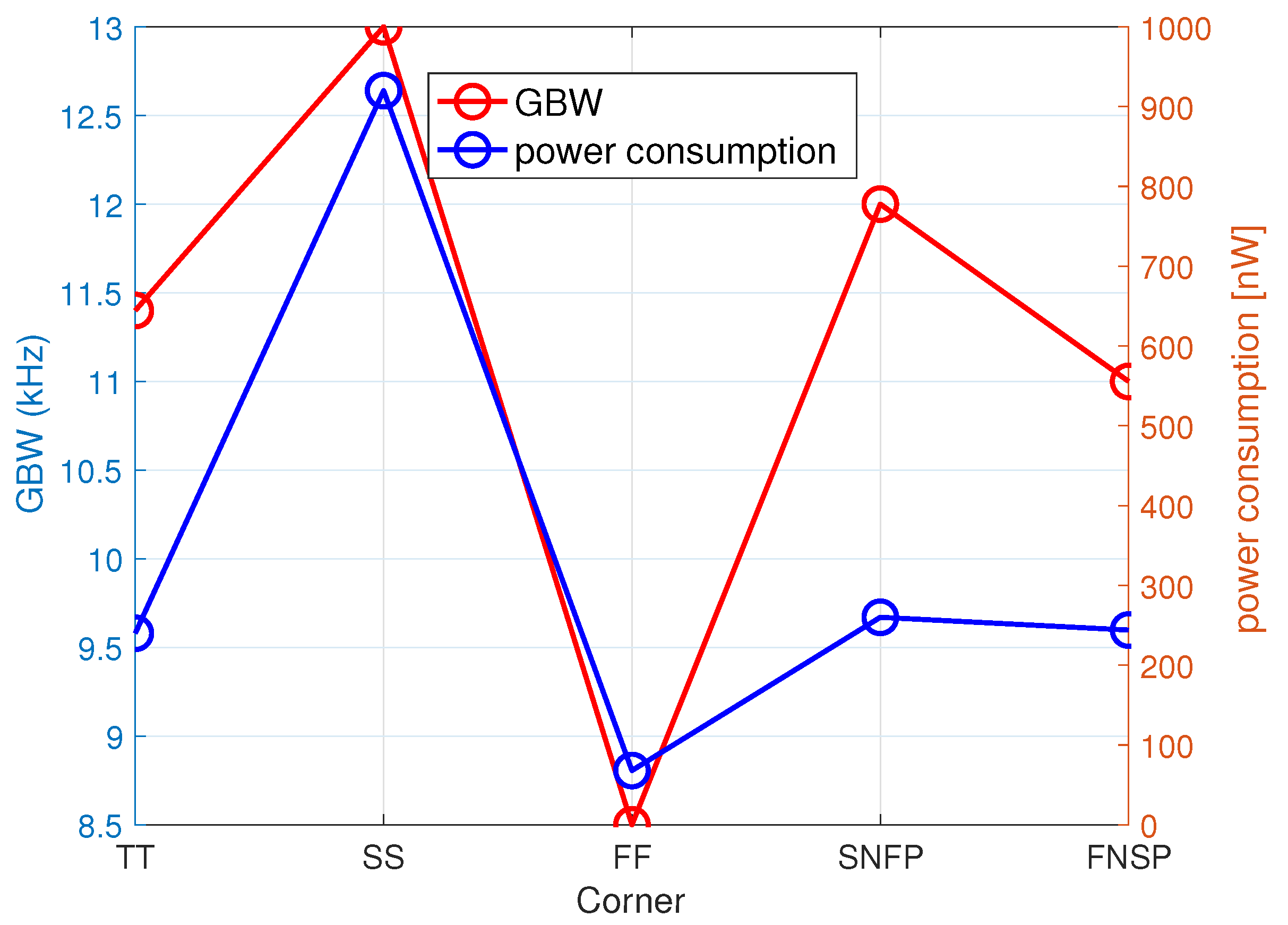
For a better readability, these characteristics are also shown in Figure 14 and Figure 15, where the gain along with the phase margin and the bandwidth along with the power consumption are plotted, respectively.
Moreover, FOM has been evaluated and it is of 1.34. This amplifier can be therefore used for ultra low voltage and low power applications, where high gain and wide common mode input range are paramount.

3.7. NMOS-only Amplifier

The nMOS-only amplifier was designed in UMC180 nm technology using the regular threshold transistors and a voltage supply of 1.8 V. A gain larger than 30 dB is required. As already stated the gain is approximately given by the ratios of the transconductances, therefore the transistors must be properly sized. Two different designs are considered, simulated and compared. In the first, all the transistors work in the saturation region, while in the second one, the transistors M9, M11, M13 and M15 operate in subthreshold. The second sizing, listed in Table 9, is the most effective and shows the largest voltage gain.
Matching issues are considering for the transistors M5, M6 and M4, M7 which are, respectively, the input pair and its active load. The internal capacitor for the frequency compensation C C is implemented by using the metal5-metal6 capacitor provided by the UMC 180 nm process. It occupies a large area, about the half of the final layout, which is of about 200 μ m × 80 μ m. The equivalent circuit extracted from the layout view has been simulated and the corner analyis was also performed. The main results are summarized in Table 10. It is worth noting that the corners are two (slow and fast) because the amplifier is made by only nMOS.
Generally, the amplifier exhibits good GBW and stability and a medium-low voltage gain compared to the topologies based on complementary devices. Neverthless, its FOM is rather low: its value is 0.2.

4. Discussion

The amplifiers presented, designed and simulated in the above sections are discussed and compared. They can be divided in four main categories: inverter-based, bulk-driven, rail-to-rail and classical topologies with non-standard improvements. In the first category, one can consider the (1) simple inverter-based digital amplifier [3], the (2) tunable amplifier [1], the (3) amplifier with feed-forward compensation [2], and the one with current-starved devices [5]. In the second category, there are several topologies: for example, classical Miller amplifier with bulk-driven input pair can be considered, as in [11], as long as folded with self-cascode bulk-driven [6] and bulk-driven with cross coupled input pair and improved frequency compensation [7]. In the third category, a rail-to-rail amplifier with transistors operating in subthreshold and cross-coupled output stage is considered [9] instead of the standard rail-to-rail because the latter has a much larger power consumption. Finally, in the four category, a standard Miller amplifier with improvement in driving capacitive load without any penalty in the frequency response is considered [8] as long as a two stage, common source amplifier with nMOS-only transistors [10].
The inverter-based amplifiers are well-suited for ultra low voltage supply because they only need a couple of complementary transistors; therefore, the minimum voltage supply is equal to a double V o v e r d r i v e . If current-starved devices are added, these amplifiers are also well suited for low power applications. Generally speaking, they exhibit good voltage gain and gain bandwidth product (GBW), which make them very appealing for wireless applications as suggested in [13]. Moreover, if they are designed to have a low power consumption, as in the circuit with current-starved devices [5], they are also well-suited to energy harvesting applications [14]. The main drawback of the inverter-based topology is the extremely narrow common mode input range; moreover, the AC characteristics are strongly dependent on the Vdd, the temperature and the process. For this reason, an auxiliary circuit is added to limit the effect of the variations. . The bulk-driven amplifier are well-suited for low voltage and low power, too, although they require a voltage supply larger than the inverter-based topology. The voltage gain and the GBW are medium because they are based on the bulk transconductance gmb which is smaller than the gate transconductance gm. On the other hand they can amplify signals with a very wide common mode input range. They can be used in implantable circuits for the processing of biomedical signals and also in low voltage CMOS active filter, as in [15].
The rail-to-rail topologies can reach a high voltage gain and presents a very wide common mode input range, too. Moreover they can reach a tradeoff between bandwidth and power consumption, depending on the application they are used in. They can be successfully used in energy harvesting and in low power applications, like IoT sensor nodes, [16]. The main drawback of this architecture is the increased circuital complexity and silicon area.
Among several improvements of traditional common source topology which can be found in the literature, the hybrid-mode amplifier exhibits a very good driving capability (very appealing for voltage regulator and active filter design) and the nMOS-only amplifier can be of great interest, not only for the goal of designing an extremely low voltage amplifier with nMOS native transistors, but also in advanced electronic materials, like in the organic, flexible, printed technologies [17]. These considerations are summarized in Table 11 where the amplifier topologies are compared highlighting the pro and contra. In the table also area, FOM and main applications are listed for the different architectures. It is worth adding that in the case of the current-starved inverter-based amplifier, three different values of FOM are listed: it is because they are dependent on the power supply, changing from 1.1 V down to 0.7 V, as written in Section 3.3.
For the sake of clarity, complexity means the number of transistors and of course it also refers to the resulting larger area consumption and noise; good PM means that the amplifier does not require frequency compensation.

5. Conclusions

Low voltage and ultra low voltage design is challenging for analog circuits and, among them, especially for amplifiers. Advanced amplifier topologies have been therefore investigated and compared in this paper, highlighting the benefits and the weaknesses, to help the analog designers in finding the best application-dependent solutions.

Author Contributions

All the authors have contributed substantially to the paper. A.R., L.C., Z.K.-V. have supervised the work, have provided the simulation tools and have written the paper; G.C., D.F., M.F., S.P., E.P., J.S., S.S. are graduating-five years Laurea degree-students which have designed the amplifiers and performed the experiments.

Funding

This research received no external funding.

Conflicts of Interest

The authors declare no conflict of interest.

Abbreviations

The following abbreviations are used in this manuscript:
CMOSComplementary Metal Oxide Semiconductor
UMCUnited Microelectronics Corporation
OTAOperational Transconductance Amplifier
CMCommon Mode
GBWGain Bandwidth
PMPhase Margin
CMFBCommon Mode Feedback
CMRRCommon Mode Rejection Ratio
PSRRPower Supply Rejection Ratio
FOMFigure Of Merit

References

  1. Ismail, A.; Mostafa, I. A Process-Tolerant, Low-Voltage, Inverter-Based OTA for Continuous-Time ADC. IEEE TVLSI 2016, 24, 2911–2917. [Google Scholar]
  2. Shrimali, H.; Chatterjee, S. 11 GHz UGBW Op-amp with feed-forward compensation technique. In Proceedings of the IEEE International Symposium of Circuits and Systems (ISCAS), Rio de Janeiro, Brazil, 15–18 May 2011; pp. 17–20. [Google Scholar]
  3. Coccoli, A.; Richelli, A.; Redouté, J.M. EMI Susceptibility of a Digitally Based Analog Amplifier in a 180-nm CMOS Process. IEEE TEMC 2016, 58, 1236–1239. [Google Scholar] [CrossRef]
  4. Bazes, M. Two novel fully complementary self-biased CMOS differential amplifiers. IEEE JSSC 1991, 26, 165–168. [Google Scholar] [CrossRef]
  5. Wilson, W.; Chen, T.; Selby, R. A Current-Starved Inverter-Based Differential Amplifier Design for Ultra-Low Power Applications. In Proceedings of the 2013 IEEE 4th Latin American Symposium on Circuits and Systems (LASCAS), Cusco, Peru, 27 February–1 March 2013; pp. 1–4. [Google Scholar]
  6. Ferreira, L.H.C.; Pimenta, T.C.; Moreno, R.L. An Ultra-Low-Voltage Ultra-Low-Power CMOS Miller OTA With Rail-to-Rail Input/Output Swing. IEEE TCAS-II 2007, 54, 843–847. [Google Scholar] [CrossRef]
  7. Kim, T.-W. A-250 mV supply-voltage 65 dB-gain OTA with an enhanced bandwidth and a reduced compensation-capacitor. In Proceedings of the 2018 International Conference on Electronics, Information, and Communication (ICEIC), Honolulu, HI, USA, 24–27 January 2018; pp. 1–4. [Google Scholar]
  8. Maity, A.; Patra, A. A Hybrid-Mode Operational Transconductance Amplifier for an Adaptively Biased Low Dropout Regulator. IEEE TPEL 2017, 32, 1245–1254. [Google Scholar] [CrossRef]
  9. Qin, Z.; Tanaka, A.; Takaya, N.; Yoshizawa, H. 0.5-V 70-nW Rail-to-Rail Operational Amplifier Using a Cross-Coupled Output Stage. IEEE TCAS-II 2016, 63, 1009–1013. [Google Scholar] [CrossRef]
  10. Young, I.A. A High-performance All-Enhancement NMOS Operational Amplifier. IEEE JSSC 1979, 14, 1070–1077. [Google Scholar] [CrossRef]
  11. Sbaraini, S.; Richelli, A.; Kovacs-Vajna, Z.M. EMI susceptibility in bulk-driven Miller opamp. IET EL 2010, 46, 1111–1113. [Google Scholar] [CrossRef]
  12. Venturelli, M.; Torricelli, F.; Ghittorelli, M.; Colalongo, L.; Richelli, A.; Kovács-Vajna, Z.M. Unipolar Differential Logic for Large-Scale Integration of Flexible a-IGZO Circuits. IEEE TCAS-II 2017, 64, 565–569. [Google Scholar]
  13. Kundu, R.; Pandey, A.; Ghosh, D.; Singh, J.; Nath, V. A 4.596 GHz, High Slew Rate, Ultra low Power Cascode Operational Amplifier in 45 nm CMOS for Wireless Communication. Int. J. Comput. Appl. Eng. Sci. 2014, 3, 15–20. [Google Scholar]
  14. Far, A. Amplifier for energy harvesting: Low voltage, ultra low current, rail-to-rail input-output, high speed. In Proceedings of the 2016 IEEE International Autumn Meeting on Power, Electronics and Computing (ROPEC), Ixtapa, Mexico, 9–11 November 2016. [Google Scholar]
  15. Kulej, T. 0.5-V bulk-driven OTA and its applications. Int. J. Circ. Theor. Appl. 2015, 43, 187–204. [Google Scholar] [CrossRef]
  16. O’uchi, S. 0.8-V Rail-to-Rail Operational Amplifier with Near Vt Gain-Boosting Stage Fabricated in FinFET Technology for IoT Sensor Nodes. In Proceedings of the 2015 IEEE SOI-3D-Subthreshold Microelectronics Technology Unified Conference (S3S), Rohnert Park, CA, USA, 5–8 October 2015. [Google Scholar]
  17. Chang, J.; Zhang, X.; Ge, T.; Zhou, J. Fully printed electronics on flexible substrates: High gain amplifiers and DAC. Org. Electron. 2014, 15, 701–710. [Google Scholar] [CrossRef]
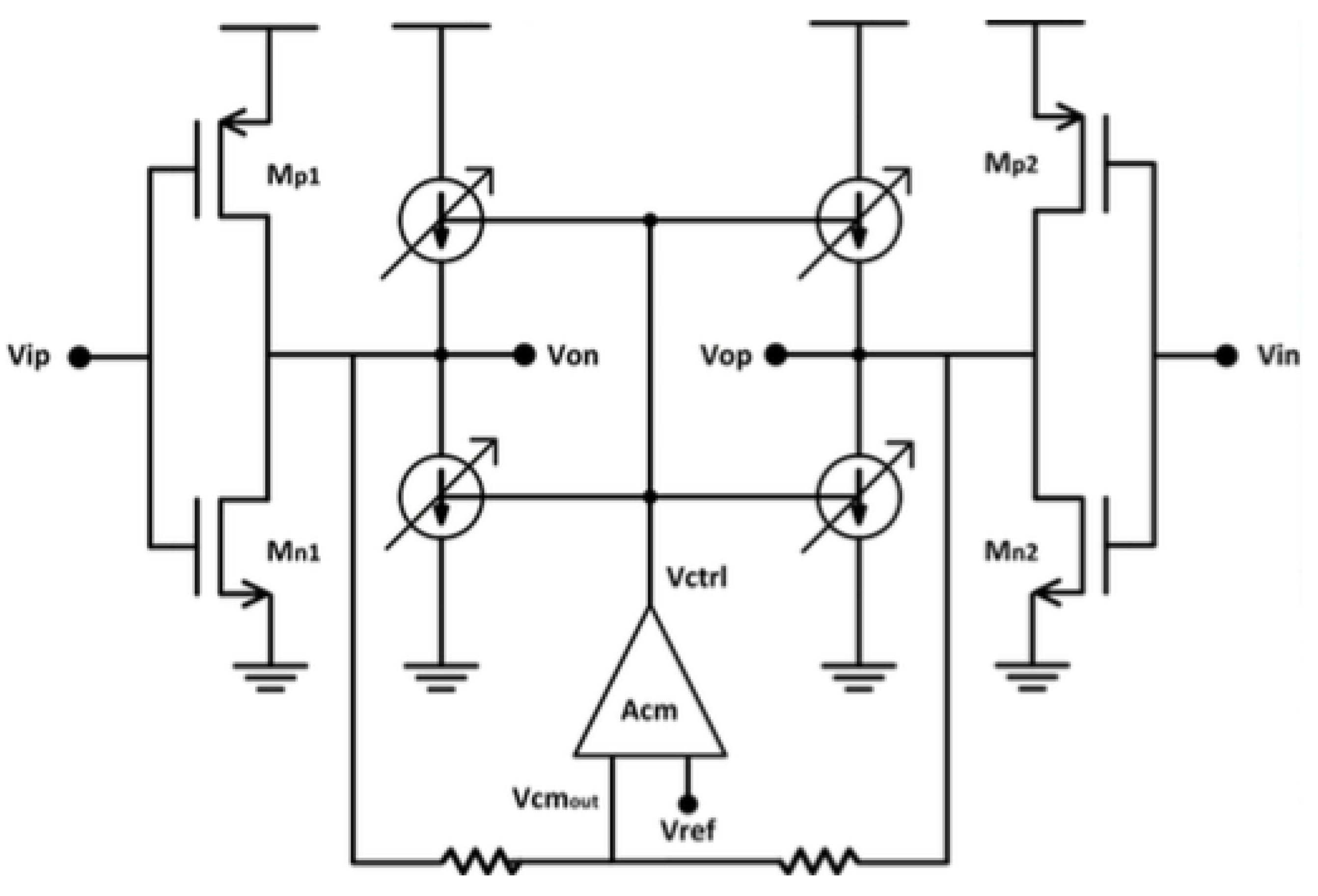
Figure 1. Tunable inverter-based amplifier.
Jlpea 08 00022 g001
Figure 2. Schematic of the CMFB.
Jlpea 08 00022 g002
Figure 3. Acm amplifier.
Jlpea 08 00022 g003
Figure 4. Conceptual schematic of the inverter-based amplifier with feed-forward compensation.
Jlpea 08 00022 g004
Figure 5. Frequency compensated three stage amplifier.
Jlpea 08 00022 g005
Figure 6. N-well biasing circuit.
Jlpea 08 00022 g006
Figure 7. Current-Starved Inverter-Based Amplifier.
Jlpea 08 00022 g007
Figure 8. Bulk-driven Miller amplifier.
Jlpea 08 00022 g008
Figure 9. Schematics of CM-OTA (a), DM-OTA (b), HM-OTA (c).
Jlpea 08 00022 g009
Figure 10. Schematic of the rail-to-rail amplifier with cross-coupled output stage.
Jlpea 08 00022 g010
Figure 11. Conventional common-source output stage; cross-coupled output stage proposed in [9]; fully cross-coupled output stage.
Jlpea 08 00022 g011
Figure 12. Schematics of the nMOS-only amplifier.
Jlpea 08 00022 g012
Figure 13. Voltage gain and gainbandwidth product versus Vdd for the inverter-based amplifier with feed-forward compensation.
Jlpea 08 00022 g013
Figure 14. Gain and phase margin of the Rail-to-Rail Amplifier, simulated in the corner analysis.
Jlpea 08 00022 g014
Figure 15. GBW and power consumption of the Rail-to-Rail Amplifier, simulated in the corner analysis.
Jlpea 08 00022 g015
Table 1. Transistors’ sizing of the Tunable Inverter-based Amplifier in Figure 1.
Width [ μ m]Lenght [ μ m]Finger Number
Mn1, Mn2100210
Mp1, Mp2350224
Mi1, Mi2422
Mi3, Mi41622
Mc1, Mc2142
Mc3, Mc4442
Table 2. Main AC characteristics.
VddGainGBWPM
0.4 V8.8 dB0.6 GHz120
0.5 V49 dB2.5 GHz46
0.6 V58.6 dB5.3 GHz18
0.7 V52.9 dB8 GHz30
0.8 V48.8 dB9.9 GHz39
0.9 V45.7 dB11.5 GHz48
1 V43 dB13.1 GHz55
1.1 V41 dB14.2 GHz60
1.2 V39.6 dB15 GHz65
Table 3. Transistors’ sizing of the Current-Starved Amplifier in Figure 7.
Width [ μ m]Lenght [ μ m]Finger Number
nMOS1212
pMOS1418
nMOS2244
pMOS2122
nMOS3336
pMOS3122
N-CMFB5.57.51
P-CMFB311
Table 4. Transistors’ sizing of the Current-Starved Amplifier in Figure 7.
Vdd1.1 V0.9 V0.7 V
A v 53 dB65 dB74 dB
GBW3.6 MHz2 MHz208 kHz
Load15 pF6 pF1.8 pF
Phase margin90 90 90
CMRR233 dB180 dB211 dB
Power consumption21 μ W3 μ W137 nW
Table 5. Transistors’ sizing of the Bulk-driven Amplifier in Figure 6.
Width [ μ m]Lenght [ μ m]Finger Number
Q1, Q22.40.62
Q3a, Q4a1.50.62
Q3b, Q4b4.50.62
QP, Q52.40.62
Q660.62
Q7120.62
Q8, Q91.80.62
Table 6. Transistors’ sizing of the Hybrid-mode Amplifier in Figure 9.
Width [ μ m]Lenght [ μ m]Finger Number
M81, M821012
M84,M87, M889014
M83a, M83b4512
M89, M903018
Table 7. Transistors’ sizing of the Rail-to-Rail Amplifier in Figure 10.
Width [ μ m]Lenght [ μ m]Finger Number
M1, M21824
M3,M41124
M5, M61124
M7, M81824
MN3a, MN3b4424
MP3a, MP3b7224
MB1a, MB1b1124
MB2a, MB2b1824
NM1, NM21121
PM1, PM2, PM31821
Table 8. Corner analysis of the Rail-to-Rail Amplifier in Figure 10.
GainGBWPMPower Consumption
TT96 dB11.4 kHz61 240 nW
FF95 dB13 kHz68 920 nW
SS94 dB8.5 kHz48 68 nW
SNFP98 dB12 kHz60 260 nW
FNSP93 dB11 kHz63 244 nW
Table 9. Transistors’ sizing of the nMOS-only Amplifier in Figure 10.
Width [ μ m]Lenght [ μ m]Finger Number
M1420.56
M2240.56
M3, M8, M10, M1520.51
M4, M70.50.52
M5, M6280.54
M9, M1140.51
M1212600.556
M1360.52
M148160.534
M1613160.556
Table 10. Corner analysis of the Rail-to-Rail Amplifier in Figure 10.
GainGBWPM
TT35 dB29 MHz88
FF38 dB34 MHz34
SS29 dB10 MHz95
Table 11. Comparison between the main topologies.
Inverter-BasedBulk-DrivenRail-To-RailHybrid ModenMOS-Only
ProUltra low VddLow VddLow VddGood drivingUltra low Vdd
compatibilitycompatibilitycompatibilitycapabilitycompatibility
Good GBWWide CMWide CM
Low complexity High gainGood PM
ContraNarrow CM rangeLow GBWComplexityMedium-lowPoor AC
Dependence on Vdd gainchracteristics
of AC characteristics Complexity
Area(1)120 μ m × 40 μ m50 μ m × 20 μ m160 μ m × 40 μ m60 μ m × 40 μ m200 μ m × 80 μ m
(2) 60 μ m × 40 μ m
(3) 40 μ m × 40 μ m
FOM(1) 1.61.031.341.20.2
(2) 4.24
(3) 1.93–3.45
ApplicationsWireless appsEnergy harv.Energy harv.Voltage regul.Flexible
Energy harv.Biomed. appsIoT sensorActive filterorganic tech.