1. Security Implication of Sensor Nodes Empowered by SoC FPAA Devices
Energy constrained IoT systems, such as wearable devices, are already sensor rich and processing/computation constrained. Many portable and wearable devices are constrained by their energy-efficiency. The digital energy efficiency wall [
1] constrains the amount of signal processing possible at energy constrained nodes. One rarely has any computational resources left to consider network security, leaving devices exposed. Fortunately, many of these devices have infrequent wireless communication with very constrained command structures, but they still exhibit a system vulnerability, particularly when monitoring or controlling physical infrastructure.
Cloud-based computing removes issues of real-time embedded (e.g., fixed point arithmetic) to be done on some far away (and supposedly free) server using MATLAB style coding. As these devices rarely have any local computation, they have capability available for range of security functions, similar to larger devices. The host system must constantly transmit and receive data to perform these computations. The network connectivity must have a minimum quality at all times otherwise performance noticeably drops. These devices require high levels of security as they are completely dependent on the network for their operation. The cloud computation still has energy and infrastructure costs somewhere. As a product scales to the consumer market, these assumption that cloud is nearly free as well as always accessible often breaks down.
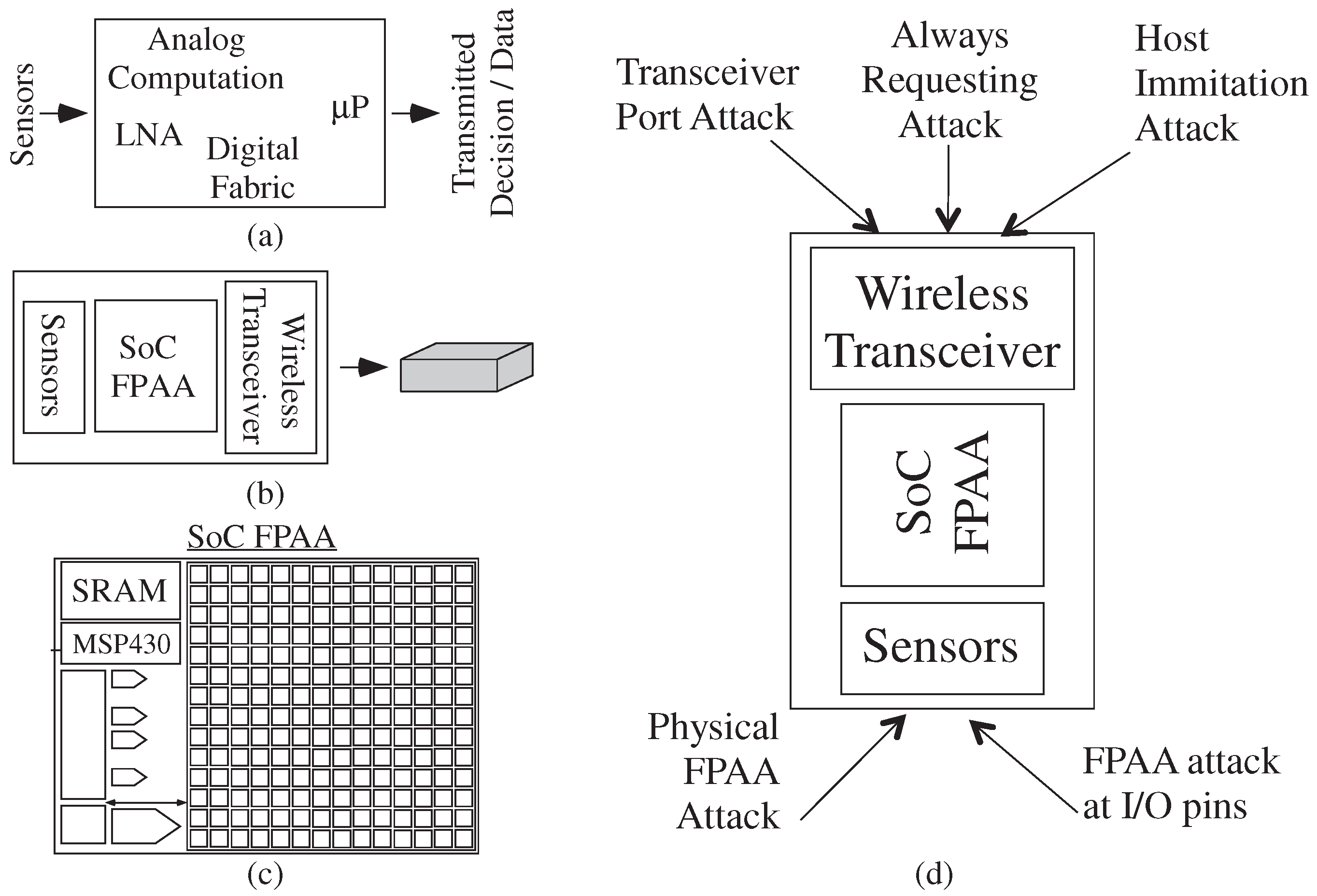
Physical computing approaches enable at least a factor of 1000 improvement in computational energy efficiency empowering a new generation of local computational structures for embedded IoT devices. Such approaches allow significant computation on these embedded platforms (
Figure 1a), making them less dependent or nearly independent of network operation. Physical computing utilizes operations over continuous-value and/or continuous-time spaces. Analog computing enables both improved computational efficiency (speed and/or larger complexity) of 1000× or more compared to digital solutions (as predicted by [
2]), as well as potential improvements in area efficiency of 100×. Without using physical computation, the embedded processor and wireless transceiver energy constraints make the sensor node a simple, low-speed data acquisition node.
Although ultra-low power Physical computing could have huge impacts for network of small autonomous sensor nodes (
Figure 1b) , these same ultra-low power physical-computing enabled nodes often require secure operation against attack (
Figure 1d). Analog Computing has emerged through the innovation of the large-scale Field Programmable Analog Arrays (FPAA) devices (e.g., SoC FPAA [
3]). Although FPAAs (
Figure 1c) are a recent technology (e.g., [
3]), widespread adoption of these devices eventually requires some level of security measures against malicious users.
The following sections begin the discussion of security opportunities for, multiple vulnerabilities of (
Figure 1d), and issues using, FPAA devices for small embedded IoT platforms. Security, and resulting privacy concerns [
4], particularly as people believe they are being watched [
5], are a fundamental concern of small, low-power ubiquitous computing nodes [
6]. We start by reviewing FPAAs as physical computing devices for low-power embedded applications (
Section 2). These FPAAs enable devices for low-power context-aware computation (
Section 3), particularly in their utilization of communication, the typical path for insecure operation. The conversation moves to secure FPAA devices (
Section 4), showing positive FPAA Security attributes (
Section 4.1), and addressing FPAA security issues (
Section 4.2). FPAA devices can be part of the resulting secure computation, such as implementing unique functions (
Section 5).
Section 5 discusses using the FPAA infrastructure to build a unique function for security, as part of FPAA device security. FPAAs open new opportunities to investigate security of analog/mixed signal ICs (
Section 6). The final section summarizes the discussions as well as recommends approaches for secure embedded FPAA devices.
2. FPAAs as Physical Computation Devices
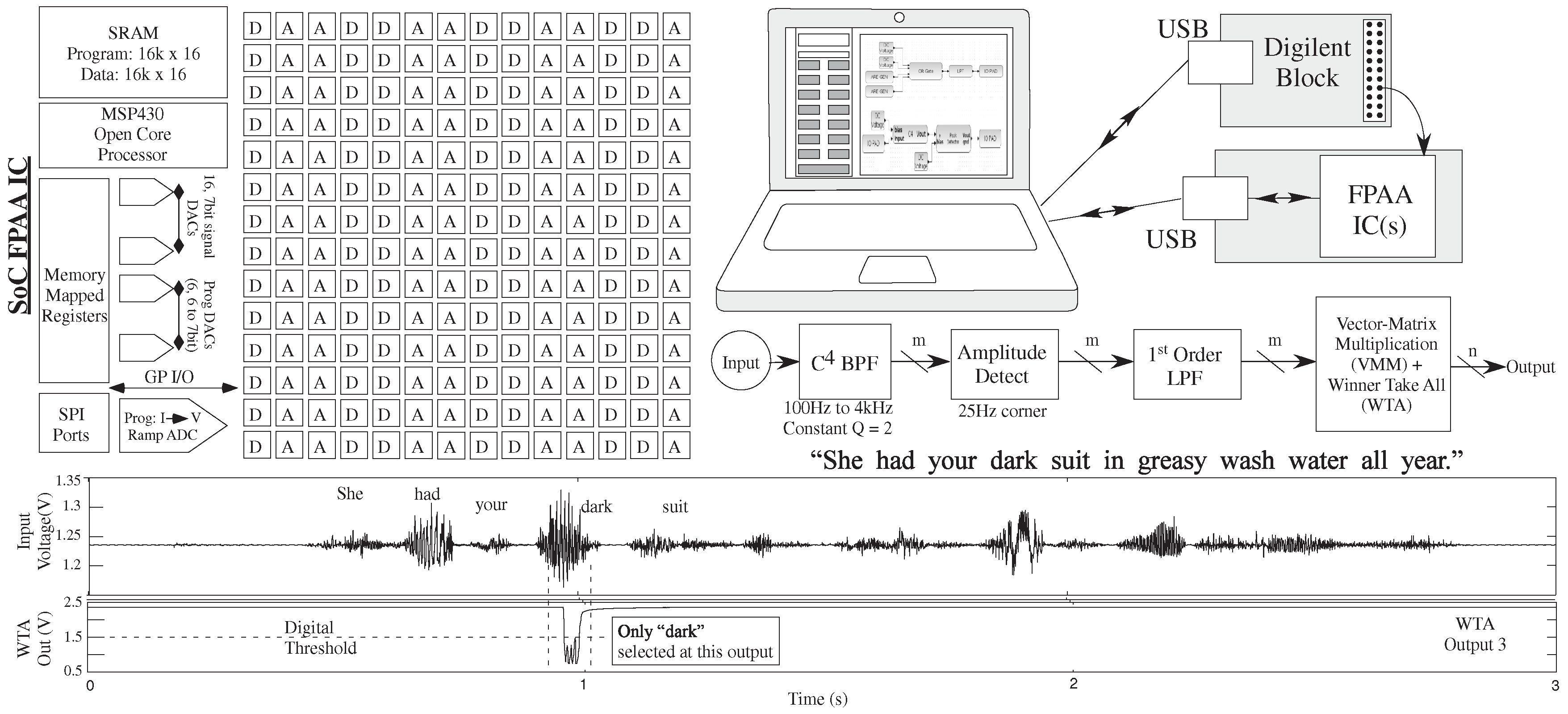
FPAA devices are our vehicle for discussing ultra-low energy computing (
Figure 2). FPAA devices allows the user to investigate many physical computing designs within a few weeks of time. The alternative for one design would require years of IC design by potentially multiple individuals. These FPAAs compare favorably against custom designs, and unlike FPGA designs, FPAA architectures are open to the academic community.
The SoC FPAA [
3] ecosystem (
Figure 2) represents a device to system user configurable system. An SoC FPAA implemented a command-word acoustic classifier utilized hand-tuned weights demonstrating command-word recognition in less than 23
W power utilizing standard digital interfaces (
Figure 2) [
3]. Multiple analog signal processing functions are a factor of 1000× more efficient than digital processing, such as Vector-Matrix Multiplication (VMM), frequency decomposition, adaptive filtering and classification (e.g., [
3] and references within). Embedded classifiers have found initial success using this SoC FPAA device towards command-word recognition [
3], and accoustic (and biomedical) sensor classification and learning (e.g., [
7]) in 10–30
W average power consumption. The circuits compute from sensor to classified output in a single structure, handling all of the initial sensor processing and early stage signal processing. This ecosystem scales with newer ICs built to this standard, as expected by all future FPAA devices [
8].
Floating-Gate (FG) devices empower FPAA by providing a ubiquitous, small, dense, non-volatile memory element [
9]. A single device can store a weight value, compute signal(s) with that weight value, and program or adapt that weight value, all in a single device available in standard CMOS (e.g., [
3]). The circuit components involve FG programmed transconductance amplifiers and transistors (and similar components) with current sources programmable over six orders of magnitude in current (and therefore time constant) [
10]. Devices not used are programmed to require virtually zero power. FG devices enable programming around device mismatch characteristics, enabling each device in a batch of ICs to perform similarly.
3. Low-Power Context-Aware FPAA Architectures
The need for low average power consumption requires that higher power devices, like wireless transceivers and even embedded
P, must be shut down most of the time. Digital communication typically dominates the overall energy consumption [
11]. These devices should be active only in those rare cases where they are needed, such as when messages need to be passed between nodes. Similarly high power sensors and actuators (e.g., acoustic speaker) needs to be shut down except when it is being used.
The FPAA enabled sensor node (
Figure 1) classifies (e.g., [
3]) and learns from original sensor signals, performing all of the computation, classification, and learning required, and operating the entire system in its real-world application environment. FPAA devices allows the user to investigate many physical computing designs within a few weeks of time. The alternative for one design would require years of IC design by potentially multiple individuals.
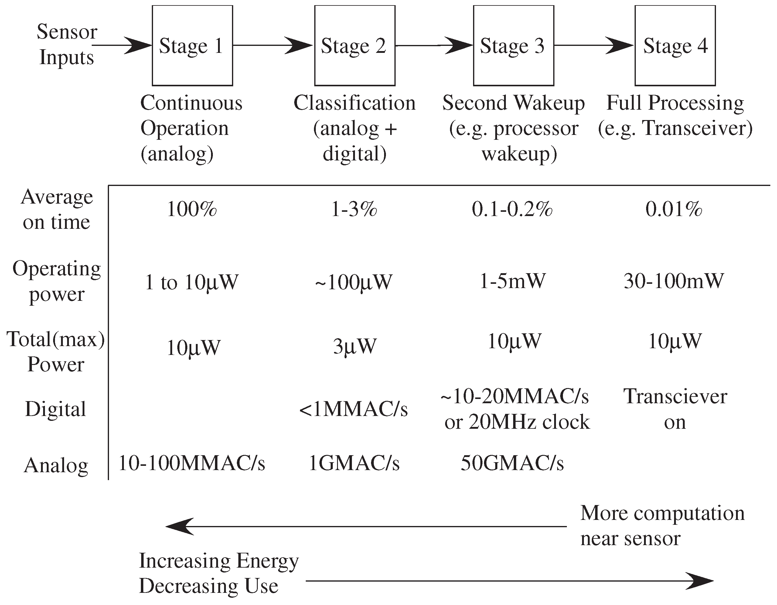
Figure 3 shows the comparison of energy required at each level, as well as the computational power available at each stage for different computing block types. The always-on computation in stage one requires being physical computation, both because of its computational power as well as its close proximity to sensor inputs. FPAAs enable small ultra-low power physical computing devices capable of computational-intensive (>10 MMAC(/s)) context-aware processing. This approach requires low-power components, continuously operating or operating frequently, that can decide when to
wake up the expensive hardware components.
Physical computing in context-aware architectures enables potential energy harvesting opportunities, but further constraining potential device security techniques.
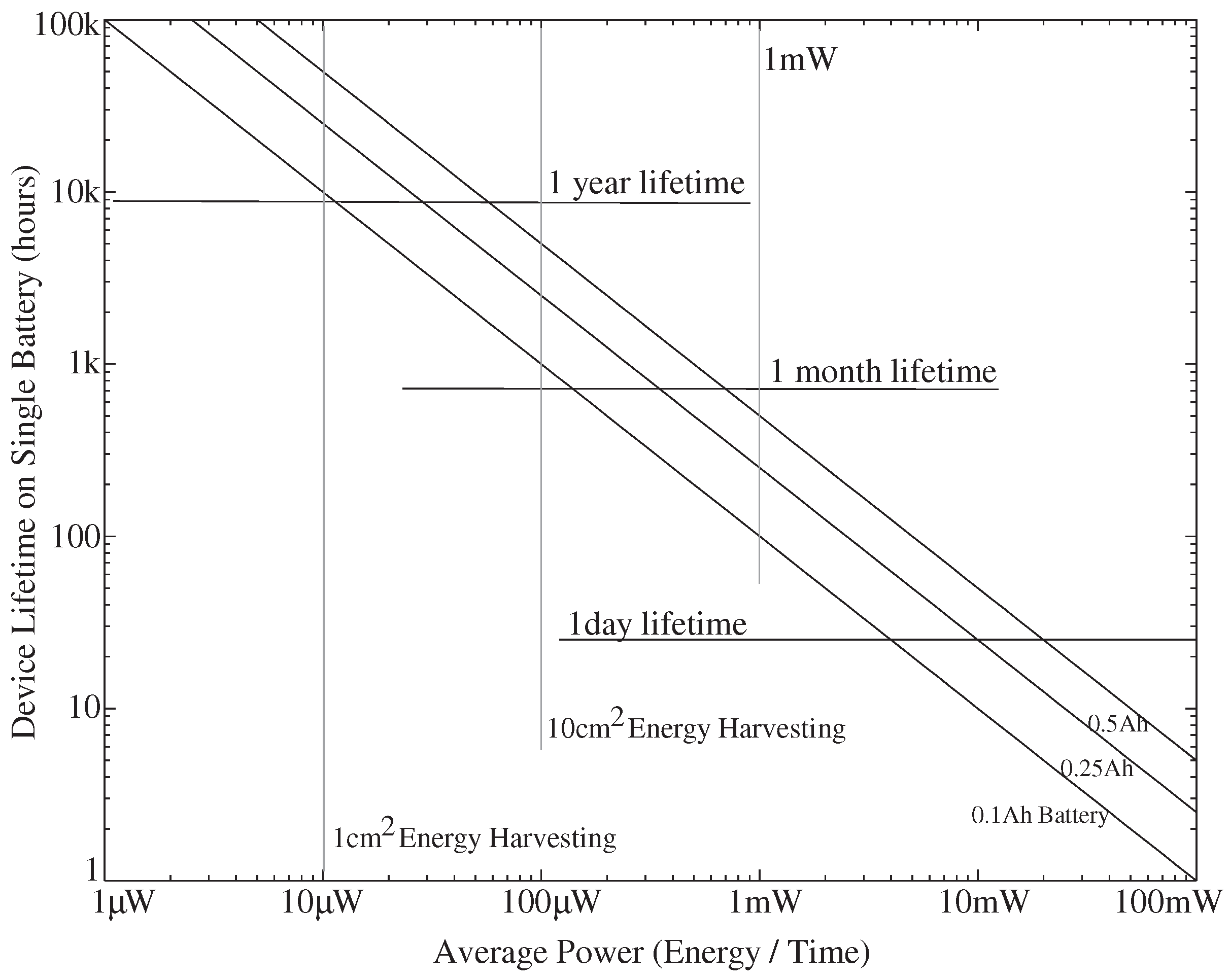
Figure 4 shows the typical breakdown for a context-aware node computation with a 100
W power budget. The node requiring 100
W average power could operate for a several months on a single battery. These physical computing components are enabled by the ×1000 energy improvement (and x100 area improvement). Most energy harvesting devices supply ≈10
W of power per cm
except in unusual environments.
Figure 4 shows the device lifetime (due to average power consumption) for a single coin cell battery (0.1–0.5 Ah). A 10 cm
energy harvesting device could supply 100
W of average power, a manageable area for an embedded sensor node. Energy harvesting requires a number of straight-forward regulators and circuits [
12], infrastructure mostly built on the SoC FPAA IC [
3].
4. Embedded FPAA Security Concerns
IoT devices require considering security issues to decrease the possibility of a successful attack on the device [
13]. These issues can include exploiting an IoT system to get advantage (e.g., financial) over other systems [
14], creating backdoor access with insecure interfacing or debugging modes [
15], enabling access to a range of applications (e.g., quadcopters [
16]). These issues get appreciably more difficult for small IoT nodes, often having some device power constraints, and as a result present unique security threats [
17].
The very opportunities of FG enabled FPAA ICs make them potentially vulnerable to attack. Energy efficient computation results in lower traditional resources for security. The FPAA opportunities presented in the last section, particularly the ultra-low energy and small size characteristics, require consideration to make these embedded nodes secure. This section discusses multiple opportunities towards secure FPAA devices.
Section 4.1 and
Section 4.2 discuss the positive characteristics and security issues, in turn, for the FPAA device family.
4.1. Positive FPAA Security Attributes
The FPAA structure has a number of good security aspects. The FPAA uses FG devices to store the device state without any SRAM loading vulnerability, particularly from an external IC. Once the FG values on the chip are programmed loaded the FPAA code is secure, unless one can scan out the states of the FG elements. FG programming an IC will have minimal changes over the lifetime (e.g., 10 year rating) of the part. The programming code is not the IC P SRAM, but only used for programming, then purged after programming. Analog values hard to measure without disturbing the values significantly, and digital computation can be encoded with analog computation and storage. Further, very low power circuits are challenging to externally measure due to the low circuit currents (e.g., pA and nA). These transistors do not have enough current or field to generate light to measure transistor behavior, and become very hard to measure the external fields.
On the other hand, the FPAA structure is a platform for creating secure applications. The SoC FPAA structure is a generic structure, openly published, and built from general components. None of the particular components are unknown or confidential. IC Layout says almost nothing about the programmed IC function. The motivation to
steal the knowledge of on-chip FPAA circuits is minimal. The infrastructure can measure the analog behavior at any given node in the FPAA. FPAAs allow for scanning every hardware node internally to the circuit (e.g., [
3]). If the core FG programming on the IC is verified, effectively part of the calibration procedure and measurement [
18], then the entire IC can be verified. Secure analog and digital code can be programmed in a secure space.
The IC could have intelligence, using internal signals and voltages, to choose to erase its contents. If tampering is suspected, the operating device could pull up on the tunneling voltage line(s) in an attempt to erase the previous operating code. The device parallel erase occurs from a combination of electron tunneling and reverse tunneling. The result leaves little chance of recovering any previous code even with a short erase cycle. One is more likely to pick up device mismatch patterns rather than anything of the previous code.
4.2. Addressing FPAA Security Issues
FPAA devices are far from safe from a potential malicious agent, even with a number of good starting properties. For example, the current FPAA devices do not have encryption and related security on the input control of the device. If an actor could connect to the particular control connections, even if the IC pins are disconnected or disabled, they could get direct control of the device and programming infrastructure. Future FPAA devices will have encryption on the control structure, particularly as they move to a wider user community. The encrypted access can make use of a PUF from the particular FPAA, such as the approach shown in
Section 5. Encryption is a straight-forward solution used on secure FPGA devices [
19], with multiple papers showing FPGA implementation of secure encryption and decryption [
20].
Figure 1 illustrates possible security issues and types of attacks for an embedded system built with SoC FPAA device. Smaller IoT systems often need to address intrusion detection and resulting policy-based mechanisms for security [
17]; FPAA enabled systems take these issues to the next level. The FPAA attacks could happen by physical tampering with an existing device, as well as electronic attacks through the communication port, such as a transceiver port. A physical FPAA attack, the device is obtained while avoiding self-destruct sequence to be explicitly deconstructed. If the internal code can be obtained, likely at considerable expense, one could potentially reconstruct the FPAA function. Mismatch encoded functions would require additional computational and measurement structures. An alternate physical FPAA attack could use a compiled digital serial port to gain access to the digital control and resulting programming interface. When digital interfaces (e.g., SPI) are controlled by the processor, getting control of the processor is unlikely. A more likely situation is finding a way to stall the computation resulting from a physical attack on the clock structure. Many systems are far less secure due to physical tampering if the device has been obtained, and any self-destruct/erase mechanism was somehow avoided. A more likely situation is a non-physical attack through the transceiver interface into the IC. These can include attacks to gain control of the FPAA device to reprogram the device, or constantly attacking a device to drain the node battery power.
Low-energy computation opens application opportunities at 10 mW, 1 mW, and lower average power consumption, and yet the low power consumption constrains the system security capabilities. Embedded FPAA applications also have limited digital memory because of the system cost. Network security is characterized in terms of classes of networked devices [
21], summarized in
Table 1 [
22,
23,
24]. These numbers are framed in terms of the cost of a small IoT OS operation and maybe basic security functions [
25]. SoC FPAA is a C
device having only 32 kB total digital memory. Digital memory is expensive in terms of relative on-chip area, complexity, and energy dissipation. Many systems going forward might have less total digital memory, as well as many systems that will not rise to the C
memory level. FPAAs enables a whole opportunity of C
devices, devices many assume are impossible to secure over a network. Running a minimal OS and security code may exceed the rest of system energy budget.
So how do we have an ultra-low power secure IoT system? Part of the opportunity is coding systems outside of a minimal OS, consistent with the rest of the event-based FPAA P code, as well as enabling tight secure stack and security aspects in MSP 430 assembly language. Digital FPAA event code is coded in assembly language and encapsulated in graphical code for easy user reuse.
Network traffic attacks on FPAA-based systems are likely to be a point of vulnerability, requiring building tables and metrics of proper and improper network activity and classifying the resulting responses [
26,
27,
28,
29,
30,
31,
32,
33,
34,
35]. These functions must be done in as low computational energy as possible. The functions require as minimal digital energy in parsing and creating these tables. Classification energy would be minimized using learning classifiers compiled on the FPAA infrastructure [
7].
5. FPAAs for Unique Functions
Unique functions in FPAA IC Devices are rich platforms to construct unique functions, particularly for security. Unique functions and Physically Unclonable Functions (PUF) implement a noisy (e.g., mismatch) function [
36] to enable unique device identification and authentication [
37,
38], A Unique Function or PUF generates a response y when probed with an input x that depends on both x and the unique intrinsic physical properties of the device [
37,
39]. The FPAA device allows for the selection of many devices, devices that have mismatch specific to a particular IC, and mismatch that can be selected and compiled into a particular circuit. The mismatch between pFETs for a FG device enables almost 1 M mismatched components.
Unique mismatch of device components, whether inherent in the device or compiled into a structure, provide a secure code unlikely to be replicated by another IC.
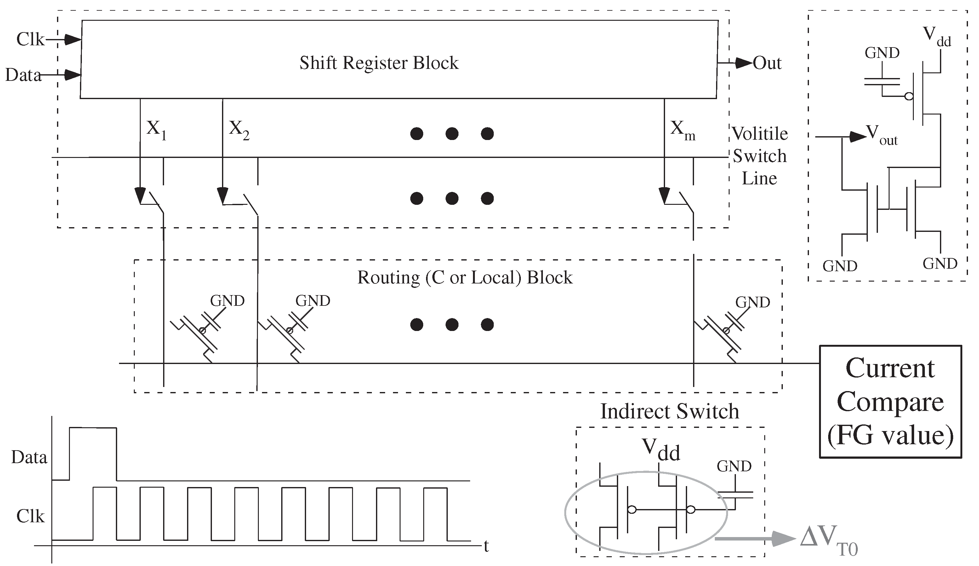
Figure 5 shows an example FPAA circuit for generating a unique function, the first compiled in and utilizing properties of an FPAA. This approach utilizes the mismatch available in the FPAA circuit, mismatch we typically remove from the device. The structure yields a code for encryption of data, enabled by programming the desired code by the user. The entire input code (stimulation) includes the address of the FG elements to measure this structure focuses after the selection, a capability built into the SoC FPAA. The initial input code addresses the right PUF device. Only one device gives the right stimulus.
This FPAA approach is similar to the FPGA approach for making unique functions and PUF, in that a function is compiled on the device and utilized to create a unique output code for a particular input stimulus code. Unique functions and PUFs have been implemented in FPGAs (digital) [
40,
41], and analog circuits [
42,
43,
44]. For example, [
41] uses delay variability in the FPGA to create a specific code directly affected by the component variability. All of these functions are based on the mismatch of the resulting device, whether custom fabricated or compiled in the structure. This FPAA approach is similar to the FPGA approach for making unique functions and PUF, in that a function is compiled on the device and utilized to create a unique output code for a particular input stimulus code.
The unique function circuit (
Figure 5) is compiled into the FPAA circuitry, where implementation and routing of other circuits might obfuscate the resulting devices. The resulting outputs, scanned through shift registers available throughout the IC, would be thresholded to yield a digital code. The FG elements would be programmed to bias the resulting code as desired, modulating the mismatch pattern. The function could be compiled right into the rest of the circuitry, where implementation and routing of other circuits would obfuscate the resulting devices.
This technique allows for an evolution of the codes through secure FG updates. One can reprogram the code if there is a concern, still using mismatch to secure the device. If a code was suspected to be discovered, one could easily just move the sensing circuitry to an open circuit area. This unique function circuit does not always live on chip, but can compiled onto a particular IC when needed. If the IC is erased, knowledge of the PUF is also erased except in the secure space originally used. For secure writing of FG devices, the configuration is extremely hard to read out if control pins are not available.
This unique function circuit output needs to be invariant under environmental changes as in temperature, supply voltage, and other electromagnetic effects.
Figure 6 shows the effective circuit to analyze for the unique function block, the circuit one would see for each FG switch current source (M1) in the chosen sequence. The CABs have a compiled nFET current mirror, and other element are switch elements. Further stages threshold the output signal, as well as communicate the signal, to other on- or off-chip digital components.
The balanced structure means, within the W/L mismatch of the nFET and pFET threshold currents, effects of supply are negligible, as well as other chip-global environmental effects. FG charge directly account for threshold voltage differences. We get a common-source circuit topology where the gain and logical threshold is independent of temperature [
45].
The circuit is symmetric with matching components. The potential combinations offer many opportunities for secure circuits build around, or hidden by, the core system functionality. The two transistors from the CAB nFET current mirror are drawn identical. All of the switch transistors are drawn identical. Two switches, which are same layout (one from a group of devices), and two nFET devices which are identical. The particular ones could be anywhere on the chip, large number of combinations. Capacitors (C) into the FG match; the potential connected to it has minimal effect, whether GND or intermediate voltage typical for temperature resistant circuits (e.g., [
45]). Source voltages are tied to
or GND, the same as their substrates, and therefore has no effect in this circuit. The FG voltages,
and
are just set by programming.
One can analyze the resulting supply and temperature effects on the circuit in
Figure 6. The MOSFET transistor model for subthreshold and near-threshold channel current (I) in saturation as a function of source (
), drain (
), and gate (
) voltages is [
45]
where
and
are the gate and drain to surface potential coupling, respectively.
is the current at threshold,
is the threshold voltage, and U
is kT/q or the thermal voltage (25.8 mV).
is typically a combination of a constant term due to charge and barrier differences and an nFET or pFET proportional to U
.
and
are weak functions of temperature (e.g., <200 ppm/C), and
is a weak power law between 0 and 1/2 of temperature. Solving KCL around
and
, we get
Subtracting these two terms, we get the large signal solution for M1, M2, M3, and M4 in saturation as
where
is directly a function of
and nearly insensitive with temperature.
and
and
and
have little change with temperature. The output is dependent on difference of threshold voltages, subtracting the temperature component, and leaving the constant mismatch terms. Even though the charge loss on a single FG device is very small, 1–100
V for 10 years, the effective charge loss on a differential FG device is significantly less, 1
V for 10 years (e.g., [
46]). FG charge directly account for threshold voltage differences. The temperature in sensitive behavior is verified by similar circuits presented elsewhere [
45]. Therefore we get a typical of common-source circuit topology where the gain and logical threshold is independent of temperature.
The circuit SNR estimates the very low resulting bit-error rate when sensing the resulting output code. The logical threshold noise, effectively, the input referred noise on , is proportional to the kT/C noise calculation at . The load capacitance would be between 100 fF and 1 pF (typical) for FPAA routing, resulting in 100–200 V total RMS noise for the smallest capacitance load. The useful FG voltage variation is roughly U for this application, resulting in greater than 40dB SNR for this comparison. The resulting Bit Error Rate (BER) for this SNR level would be negligible (<10).
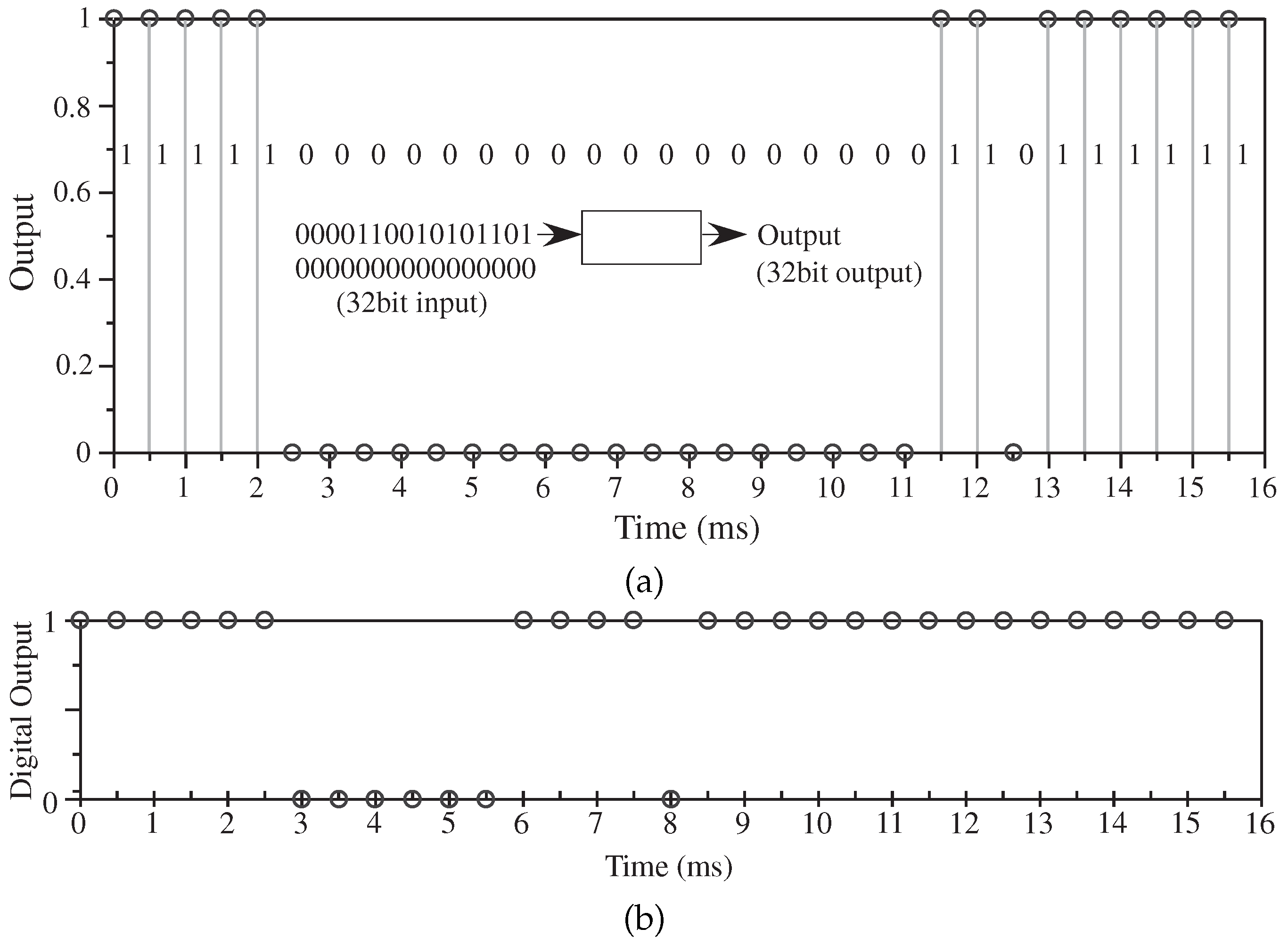
Figure 7 shows measured output from the selected unique function circuit stimulated by a 16-bit random code followed by 16
0 values. The input modulates the shift register
data values. A longer input signal is possible. The output code can be a part of the streaming output, adding additional security.
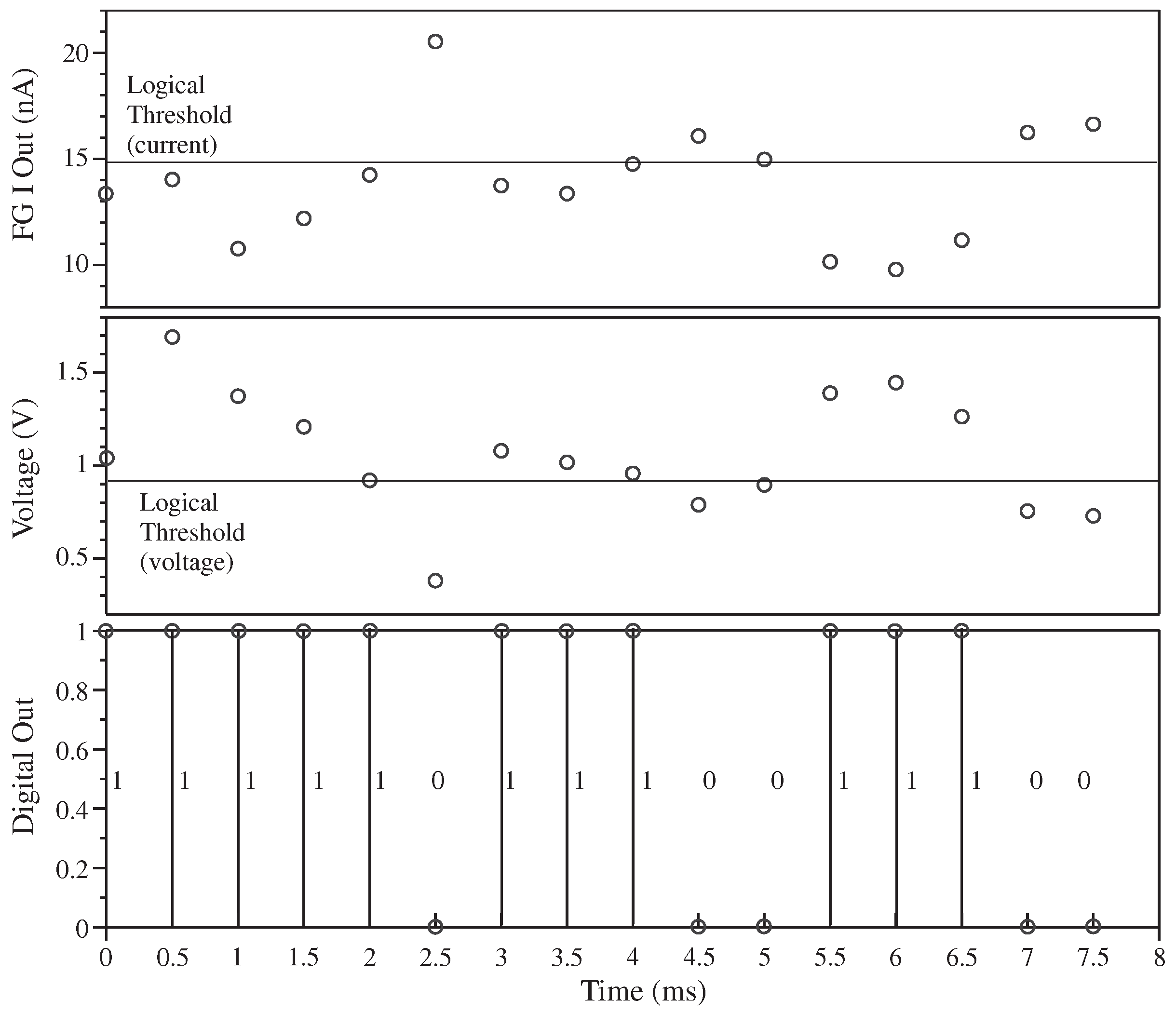
Figure 8 shows measurement of this FPAA unique function circuit. The circuit operation is illustrated using a 16 bit demonstration output code with all FG currents programmed identically. The particular bias current used is chosen by the original design, and can be any subthreshold bias current level.
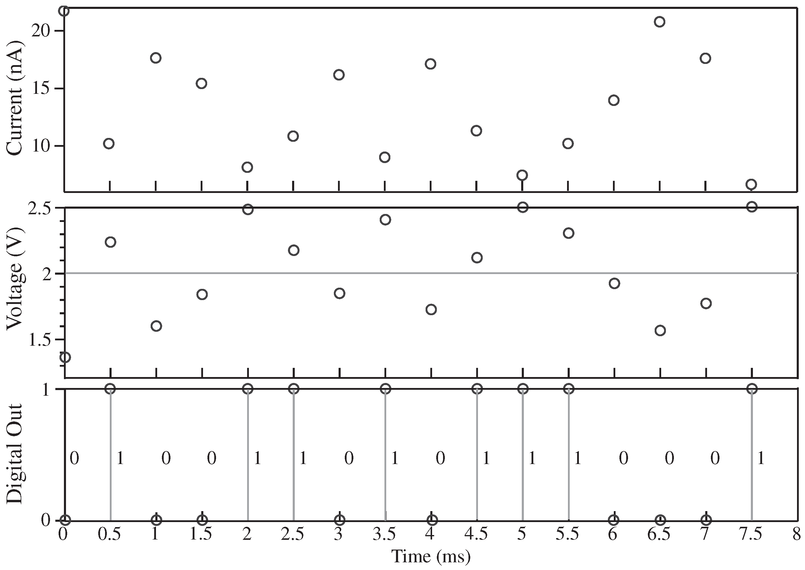
Figure 9 shows the measurement of this particular FPAA unique function circuit programmed slight variation current variation. Once the chip is programmed, one cannot tell externally.
6. FPAAs for Investigating IC Validation and Understanding Deconstructing IC Function
Deconstructing an FPAA also begins the discussion when an FPAA device is physically compromised, rather than network compromised. For the FPAA, the IC layout says very little about the actual device performance.
Embedded systems utilizing large amounts of analog computation, as well as asychronous communication (e.g., [
47]), are far harder to detect than fast clocking digital processors. The
P operation has a small part of the overall operation, typically at lower clock frequencies than most processors. The processor often is only operational for part of the computation (e.g., wakeup and clock modification on interupt event); the user should still employ good countermeasure techniques when using the processor (e.g., [
47,
48]), because some side-channel detection could be possible (e.g., [
49]).
Analog computation, as well as low-power digital logic, signals are extremely difficult to detect by side-channel approaches. Many on-chip signals, particularly analog signals, are biased with nA and pA level currents, resulting in extremely small transmitted signal power or modulations on the power supply. These signals tend to be asynchronous, further complicating detection, similar to digital techniques of adding random delays or noise [
50,
51]. The lower currents and lower operating power supply makes optical measurements extremely challanging by decreasing the high-field operation required for optical Si emission of analog and digital circuits. Digital logic gates in minimum-sized, fast clocked systems, place nFETs and/or pFETs in a high-field, high-current region during a state transition, creating high energy carriers that are optically emitted. Techniques considered during the BB exercises verified the difficulty finding these signals.
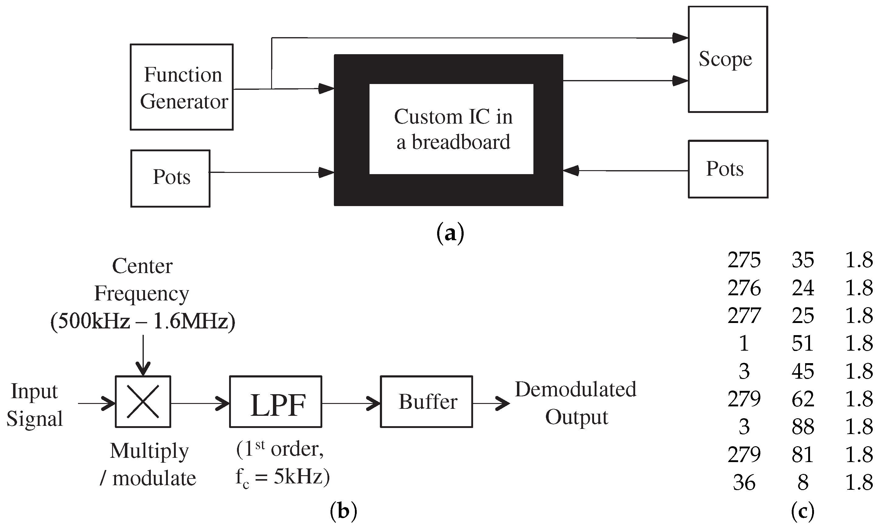
One case is reconstructing the circuit function from the resulting FG switch list. The programming representation is called a switch list (
Figure 10c); any extraction of the FG voltages is an equivalent representation. One would need to know the particular FPAA IC. One gets gets this representation by reading the programmed FG values, either because the input is not encrypted and code is downloaded to read the values, or someone employs high cost and time-intensive methods were used to read of analog FG voltages as well as characterize for indirect programming mismatches. Non-volatile analog FG storage makes discovering the internal code of a programmed device extremely difficult without huge expenses. This level of extraction is similar to having delayered an analog IC and having extracted the transistors, passives, and basic devices.
A second case is deconstructing the circuit purely from the IC pins. Even if one knows the device is an FPAA, the fabric pin connections are generic, and do not convey significant information on their own. One gets this representation when the input bitstream is not available, because the controlling bitstream is encrypted properly, likely using a unique function on the FPAA, and no particular controlling lines can be bypassed through externally applied probes. This previously programmed device just looks like a complicated ICs with pins available. This case corresponds to deconstructing an analog or mixed-signal IC from the I/O pins.
FPAA devices become good test platforms to investigate how individuals might deconstruct any particular analog or mixed-signal IC (
Figure 10). FPAA devices provide a platform for develop training and procedures for deconstructing custom ICs. The FPAA providing a structured platform to instantiate a large number of circuits and systems. FPAA devices allow for many reprogrammed circuits, so the approach can be repeated many times. The FPAA economically allows a large number of affordable deconstruction cases.
One method to understanding how much information can be extracted from FPAA pins, or how much can be extracted if basic FPAA switch-list information is available, is to have individuals attempt deconstruction of multiple FPAA circuits, and compare the approaches. Academic classroom and research spaces provide a rich exploration area.
Although deconstructing an analog IC from the package pins seems like an impossible task, with some training and some information, it becomes possible. An early example I experienced was an examination of an IC (BB Exam at Caltech (CNS 182). This particular exercise was the final exam for the second quarter (Winter quarter) for CNS 182, Analog VLSI and Neural Systems, between 1989 through 1996. I personally experienced this event both as student (1993) and teacher (1994–1996).), considered as a Black Box (BB) (
Figure 10a). The exam consisted of a two-hour lab session followed by several days (4–5) to write up the results discovered during the lab session. The students in the class spent every week for two quarters measuring custom built ICs, starting with transistors through small systems, using typical computer controlled bench equipment. When the students arrived in lab for the BB exam, a particular circuit consisting of 3–5 pins (besides power (
) and Ground (GND)) was operating correctly in one possible mode. Typically, the circuit was a single Transconductance Amplifier (TA) or 2 TA circuit with a couple of transistors, and known to be somewhat related to course topics over the first two quarters. This circuit was part of a 40-pin chip custom fabricated for the course; the students did not have access to any layout information. At least one element was a bias, set by a potentiometer. No FG devices were used. In the end, roughly half of the students would correctly guess the correct circuit with various levels of experimental justification.
The BB experience was recreated in a research environment between 2011 and 2012 using currently available FPAA devices to investigate deconstructing analog/mixed signal ICs. The FPAAs were programmed ahead of time and considered a custom IC device, and tested accordingly. The deconstruction capabilities were investigated for different amounts of IC knowledge, such as routing information or netlists. These techniques could be used to verify a desired circuit implementation, as well as search for any additional component that was placed in the circuit. The FPAAs used for these experiments were designed between 2007 to 2010 (e.g., [
52]); the results should directly extend to using the SoC FPAA devices.
A group of IC designers were trained through a set of six BB events (
Table 2) over a nine-month timeframe to eventually deconstruct a custom fabricated IC. This BB approach arose from the constant interaction between courses and research. One person designed, compiled, and experimentally characterized the design completely without the knowledge of others. The groups had no idea of the functionality of the circuits before they arrived in lab. Each person was familiar with programming and measuring the FPAA devices. Between events individuals developed additional tools to assist in deconstructing the IC design.
Different events had different level of information (
Table 2). The first case roughly doubled the number of chip pins and number of components from the historic BB case, as well as the researchers involved did not prepare before this starting exercise. The groups did a number of I-V measurements at the chip pins to identify the resulting circuit. In the second case, the groups had a switch list (
Figure 10b), similar in format to the SoC FPAA approach [
10]. The group made extensive use of the routing visualization tool, Routing Activity Tool (RAT), to uncover the resulting circuits. Whiteboard pictures prove this solution approach.
Figure 10b shows the expected demodulation circuit which all groups found; the groups also found the extra oscillator we added as well. Later cases the groups were given a form of netlist, compatible with the existing tools, for their analysis. All of the groups developed clustering algorithms to assist with grouping and identifying the resulting circuits. At each level, the speed to fully recognize and experimentally verify a particular circuit increased with the increasing circuit complexity.
The final goal was to extract and verify an entire custom IC developed by another group; the IC was eventually published elsewhere. A group of five researchers involved in the BB experiences spent three isolated days together to analyze this IC. Although the promised information varied throughout, in the end, the group was given (approximate) delayered information extracted from the IC, not including n-type or p-type selections. After three days and two additional days to write the report, the group found all four interleaved DACs (10GSPS), although only one was populated fully, Registers, digital control to pins PLL, an on-chip oscillator (VCO). The group also discovered an error on the VCO due to a misplaced GND line.
This process showed FPAAs could be used to train individuals to deconstruct the circuitry on a particular device, as well as important insights to secure a particular FPAA device. Further studies will bring out further insights to develop secure FPAA devices as well as analog/mixed-signal components.
