Article

An Ultra-Low Power 28 nm FD-SOI Low Noise Amplifier Based on Channel Aware Receiver System Analysis

by
Jennifer Zaini-Desevedavy
1,2,*,
Frédéric Hameau
1,
Thierry Taris
2,
Dominique Morche
1 and
Patrick Audebert
1
1
CEA, LETI, MINATEC Campus, 38054 Grenoble, France
2
IMS Laboratory, University of Bordeaux, 33405 Talence, France
*
Author to whom correspondence should be addressed.
J. Low Power Electron. Appl. 2018, 8(2), 10; https://doi.org/10.3390/jlpea8020010
Submission received: 25 March 2018 / Revised: 11 April 2018 / Accepted: 13 April 2018 / Published: 16 April 2018
(This article belongs to the Special Issue CMOS Low Power Design)

Abstract

:
This study investigates the benefit of an optimal and energy-efficient reconfiguration technique for the design of channel-aware receiver aiming Internet of Things (IoT) applications. First, it demonstrates the interest for adaptive receivers based on an estimation of the received power and compares the proposed channel-aware receiver with the State Of the Art. It is shown that the lifetime of the Wireless Sensor (WS) battery can be extended by a factor of five with the optimization of operating points of the tunable receiver while maintaining similar performances than industrial modules. The design of an Ultra-Low Power (ULP) inductorless Low Noise Amplifier (LNA), which fits the low power mode of the tunable receiver, is then optimized and described. The back-gate biasing of Fully Depleted Silicon-On-Insulator (FD-SOI) technology to lower the power consumption by more than 25% still maintaining performances is evaluated. The proposed LNA has been implemented in ST-Microelectronics 28 nm FD-SOI Technology, its active area is only 0.0015 mm2. The measured performances at 2.4 GHz exhibit more than 16 dB of voltage Gain (Gv), 7.3 dB of Noise Figure (NF), and a −16 dBm Input referred third-order Intercept Point (IIP3). The LNA consumes 300 µW from a 0.6 V supply.

1. Introduction

Communicating objects are inviting themselves into daily life leading to a digitization of the physical world. Based on the Ericsson annual report of 2010 [1], the world went through a turning point for mobile communications which gave rise to a massive development of connections (more than 50 billion connections are expected this year). Objects are now connected to the Internet services, able to recognize their environment, organize themselves into networks, or interact with humans. Internet of Things (IoT) is totally shifting the way people interact with their surroundings. The wide development of sensors for IoT applications means wireless communicating nodes with reduced form factor for an easy distribution in the environment and reduced power consumption for an extended lifetime. These emergent technologies unveil new constraints for integrated circuit design.
Wireless internet-connected objects will need high overall performance to guarantee the Quality of Service (QoS) of specific standards along with a small power consumption. Hence, challenges in Radio Frequency Integrated Circuit (RFIC) designs for IoT applications are multiples: reducing the form factor of these communicating nodes in order to reduce the cost of these objects, saving power consumption to increase the battery lifetime and fitting the performance requirements. Further deployment of communicating objects demands a smart use of the available power budget in order to be energy efficient. This power efficiency is therefore becoming the most important design target in IoT Radio Frequency Integrated Circuits (RFICs) for long lifetime Wireless Sensor Networks (WSNs).
The power consumption of a node is shared between the radio communication part, the MicroController Unit (MCU), and sensors with more than 70% dedicated to the radio part, as illustrated in Figure 1 [2]. Because the radio module is the most power hungry element of a node, it is of importance to further reduce the power consumption of Ultra Low Power (ULP) transceivers.
Figure 2 reports on the distribution of the DC power contribution in the transmitter and receiver parts [3]. The most power hungry block of a transmitter is the frequency synthesizer whereas the RadioFrequency (RF) amplification path along with the frequency synthesis account for more than 65% of the overall power consumption in a receiver.
Usually, the power consumption of the transmitter is overriding the power consumption of the receiver. For that reason, tunable transmitters based on the modulation of the transmitted power for an adaptation of the needs have been widely developed. In IoT applications, as listening sensors for instance, the receiver power consumption can dominate and this is why this work concentrates on adding smart tunability to the receiver in order to optimize its energy efficiency.
The manuscript is organized as followed. The next section presents the motivation of the work to better understand the need of adaptive receivers for IoT. Then, the State Of The Art of tunability techniques on existing receivers is presented. Finally, the proposed approach of channel aware adaptive receiver is described. Section 3 presents a system optimization of such channel aware receiver. The methodology to define the best thresholds of reconfiguration for better energy efficiency on the receiver is also proposed. Section 4 concentrates on the design of an ULP Low Noise Amplifier (LNA) which could fit to the specifications of the low power mode. The Fully Depleted Silicon-On-Insulator (FD-SOI) technology is then evaluated as a way to further reduce the power consumption without degrading the performance.

2. Adaptive Receivers for IoT Applications

2.1. Motivation

The explosion of multimedia wireless applications for consumer electronics makes the power consumption a key metric in the design of multi-mode wireless portable devices. Conventional transceivers have fixed performances and are designed to meet high performances in all wireless link conditions. However, most of the time, the channel is not at worst case and these transceivers are therefore over specified. Being aware of the channel link conditions would allow such devices to adapt themselves and to reduce significantly their power consumption. However, the challenge is that the QoS (Quality of Service) of adaptive transceivers should be equivalent to the one offered by conventional ones, to stay competitive. As an example, neither the communication range nor the response time can be degraded. Therefore, the sensitivity of the proposed receiver has to be equal to the sensitivity of today’s products.
Based on this requirement for channel aware transceivers, this manuscript proposes an adaptation technique for the design of a tunable receiver which can always operate at the edge of needed performance and thus, at the minimum of power consumption while keeping the needed QoS.

2.2. State of the Art Adaptive Receiver

Different power reduction and adaptation strategies have already been proposed in the state of the art. A first well-known solution is to resort to wake-up radio. This technique consists of adding a supplemental receiver in parallel of the main receiver. Its goal is to listen to the channel and to switch ON the main receiver only when a communication request has been done. In [4], a wake up radio design is proposed consuming only 52 µW. It shows that a wake up receiver is a good solution to reduce drastically the power consumption of the receiver. However, to decrease this consumption, the sensitivity is degraded to −72 dBm with 100 kbps of data rate. It is therefore impossible to detect distant communicating node. This approach is very interesting to decrease the power consumption of short range communication but does not fulfill the high QoS requested by the standards.
New solutions to save power on the RF communications have also been developed at MAC or network level such as energy efficient protocols where the transmission data rate can vary when the sensitivity of the node is reduced [5]. A low power adaptive digital baseband for standard IEEE 802.15.4 through a variation of word length and sampling frequency is presented in [6]. However, these approaches address mainly digital baseband. This is indeed particularly interesting but to be fully energy efficient, tunability has to be added to the analog-RF part of the receiver which consumes a significant part of the power. Only few works have been achieved in that area. As an example [7] is investigating the interest of a power-reconfigurable ADC. It shows a power reduction by a factor of 25 using this reconfigurable ADC. In [8], the authors shows that a fully reconfigurable LNA could considerably decrease the power consumption of the receiver through a behavioral modeling of building blocks for two standards: Bluetooth LE and IEEE 802.15.4. These works confirms the interest of the approach but unfortunately they are limited to system simulation which does not confirm the feasibility of the concept. Both system simulation and circuit’s proof of concept are needed to validate it.
Some other papers have gone a step further. In [9] the benefits of a receiver with dynamic adaptation to channel conditions is demonstrated. The methodology enables a self-learning of its power consumption and performance configurations based on real-time estimation of the channel conditions. With their artificial neural network learning techniques, the authors demonstrate that this continuous tuning reduces the power consumption. However, the maximum reduction factor of the receiver is 2 which really limit the tuning of the circuit. Moreover, the learning algorithm added to the receiver makes it more complex and reduces the interest of the adaptability.
This limited power consumption scalability is due to the fact that designing adaptive analog or radiofrequency building blocks is particularly challenging. Indeed, in power efficient analog circuit design, the current flowing through the transistor can only be modified in a limited range and this has generally strong impact on performances. Therefore, most of the time, the power consumption of adaptive analog blocks does not scale significantly (a scaling factor of five to ten is needed to justify the interest of tunability). Moreover, the figure of merit of these blocks usually degrade significantly when applying tunability. This can be observed in existing products. As an example, Atmel has shown in interest in adaptive receiver by offering some tunability is some existing modules just like the AT86RF233. In standard mode, it offers a −91 dBm sensitivity while consuming 10.5 mW. The power consumption can be decreased down to 8.5 mW while degrading the sensitivity to −49 dBm. This means that 42 dB degradation of the sensitivity is required to save 20% of the power which makes the efficiency of the tuning very low.
Therefore, this work concentrates on the development of an optimal and energy-efficient reconfiguration technique which enables equivalent performance of industrial modules but significantly increases the battery lifetime.

2.3. Proposed Approach

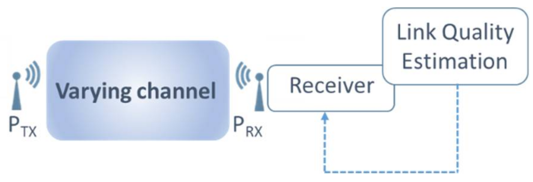
The basic principle is depicted in Figure 3. The transmitted signal PTX reaches a receiver PRX, with various channel path length, attenuation and delay. At the receiver side, the environment conditions of the channel is estimated thanks to the Link Quality Estimator (LQE). Different LQE can be exploited (RSSI, BER, etc.). After processing, the required performances are selected and the tuning information are send back to the analog and RF blocks which scale their performances and power.
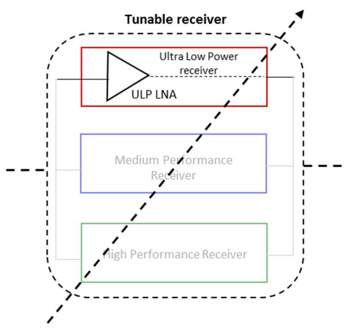
Then, in this approach, we propose to circumvent the adaptability challenge of the RF blocks by having several receive chains of various performances in parallel as shown in Figure 4. The high performance mode receiver guarantee the QoS and the medium and low performances permit to save power consumption in relaxed channel conditions. Therefore, with several receivers in parallel the tunability becomes discrete and offers fast and simplified adaptive algorithm.
The LQE of the receiver can be fast enough to enable an intra-frame reconfiguration implementation. This LQE and the selection of the operating mode of the receiver can be therefore done during the synchronization preamble as illustrated in Figure 5a. Each synchronization frame starts with the highest performance level receiver. However, the operating mode can be changed very quickly after LQE. This technique, schematized in Figure 5b, enables no frame loss.
The approach has been settled but it is now mandatory to identify how many receivers are needed to be fully efficient. Moreover, the level of performances of these receivers should be identified: If the performances are too low, the receiver will never be activated, if the performances are too high, no power will be saved.
The next section proposes a methodology for this optimization. Firstly, a distribution model of the channel attenuation is derived. Secondly, receiver consumption is evaluated as a function of the targeted sensitivity. Then, the optimal number of reconfiguration modes is calculated. Finally, the best level-thresholds between the performance modes are found.

3. Proposed Channel Aware Receiver

3.1. Context of Application

In the context of the development of smart applications dedicated to smart homes or smart industries, this study considers the following hypothesis:
-
IEEE 802.15.4 ZigBee standard addressed (ISM Worldwide band at 2.4 GHz);
-
Indoor propagation channels without the presence of adjacent blocker;
-
Peer-to-peer network arrangements;
-
Random and uniform nodes locations distribution in the area;
-
Nodes communicate with their nearest neighbor(s);
-
Signal suffering from average path-loss attenuation only.
Table 1 details the basic standard specifications used for the proposed system analysis.
The proposed approach can be re-simulated and easily adapted to other propagation conditions, different network types or additional RF propagation phenomenon such as shadowing or fading effects for instance.
For an optimized position of the discrete operating points, an estimation of the probability of the received signal power and the usage time in each mode is determined. Therefore, the model of the RF propagation conditions through the channel taking into account the chosen context of application is demonstrated in next Subsection.

3.2. Probability Distribution of the Received Power

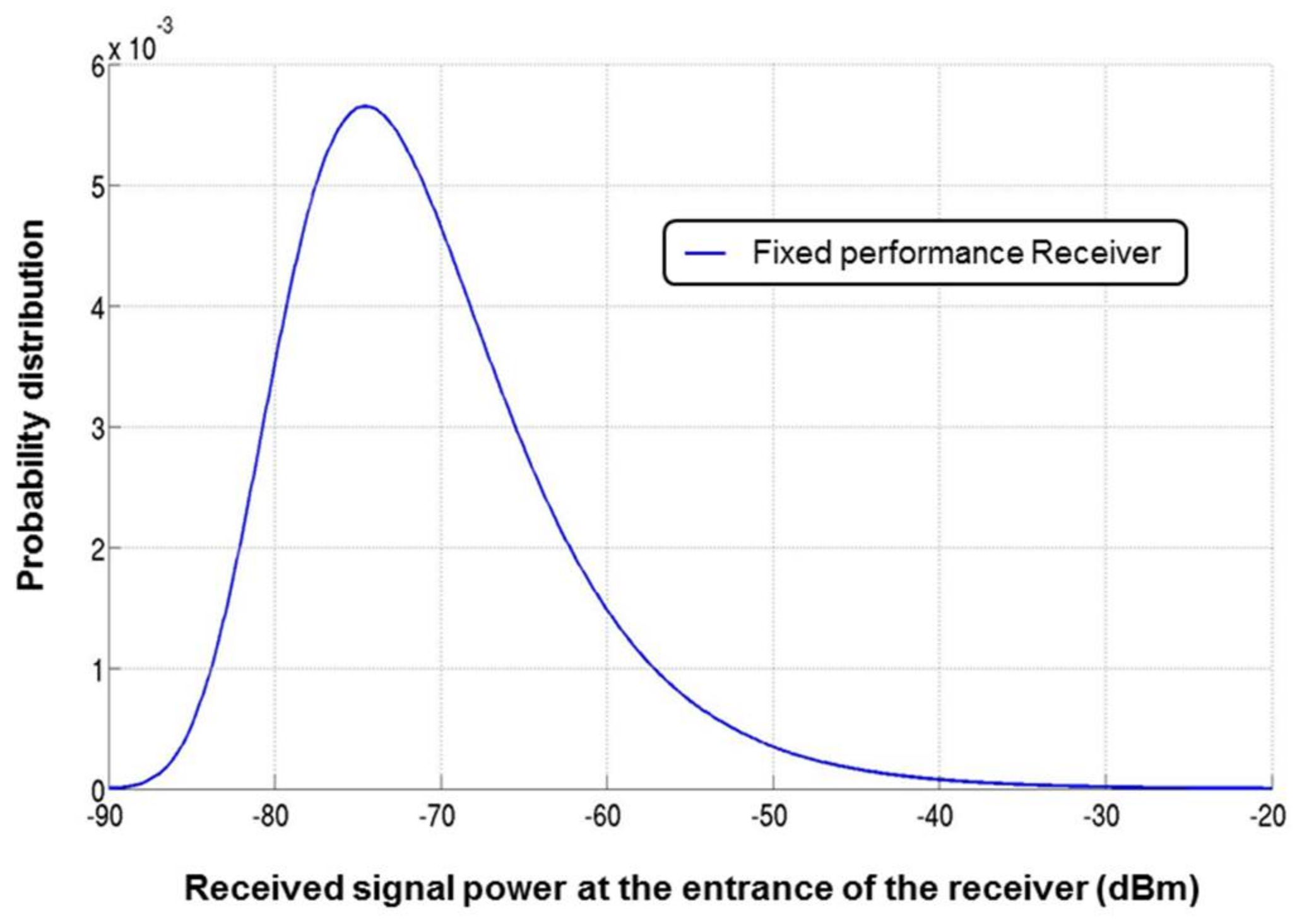
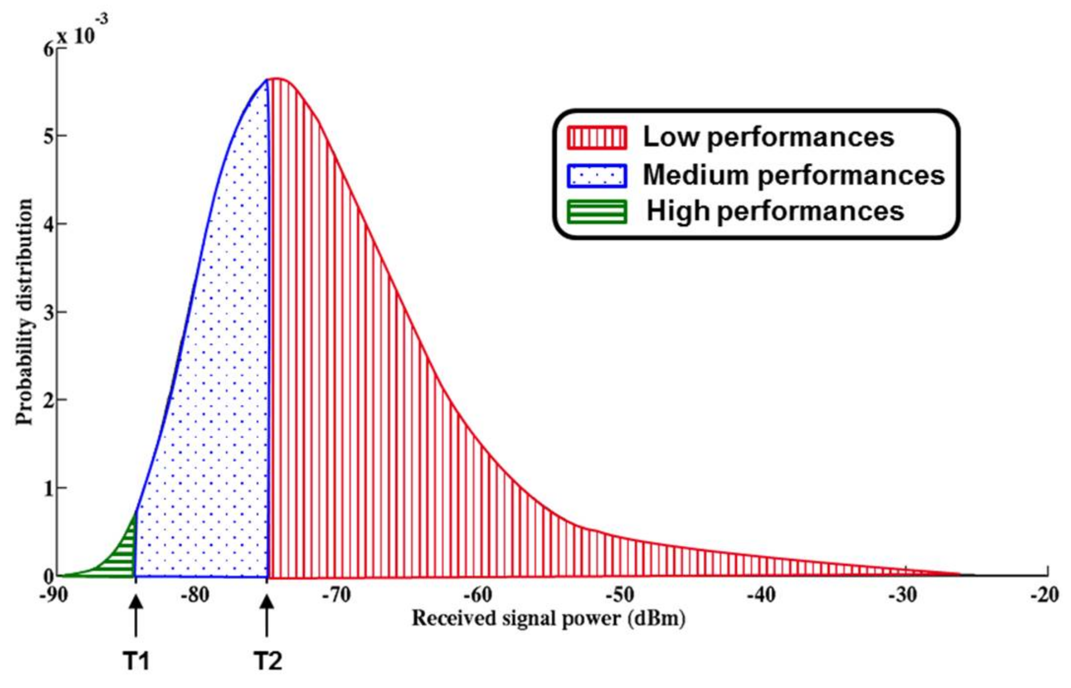
The probability distribution of the received power signal at the input of the receiver is plotted in Figure 6. The details of the calculation and the developed description of the channel conditions are presented in [10].
Figure 6 shows that the power of the incoming RF signal ranges from −90 dBm to −20 dBm. Traditional receivers would be designed to work at the worst case scenario which corresponds to the minimum of incoming signal power, −90 dBm here. However, this worst case happens scarcely as the probability to receive the minimum power signal is very small (probability close to 0). Because designing a fixed performance receiver means always respecting the QoS set by the standard requirements, a lot of power is lost when the channel conditions are not at worst case.
To optimize the operating points of the tunable receiver, a model of the receiver sensitivity versus the power consumption has to be established. The next subsection proposes an approximation of the receiver sensitivity versus its power consumption with the study of several receivers available in the literature.

3.3. Approximation of the Sensitivity and Power Consumption of the Receiver

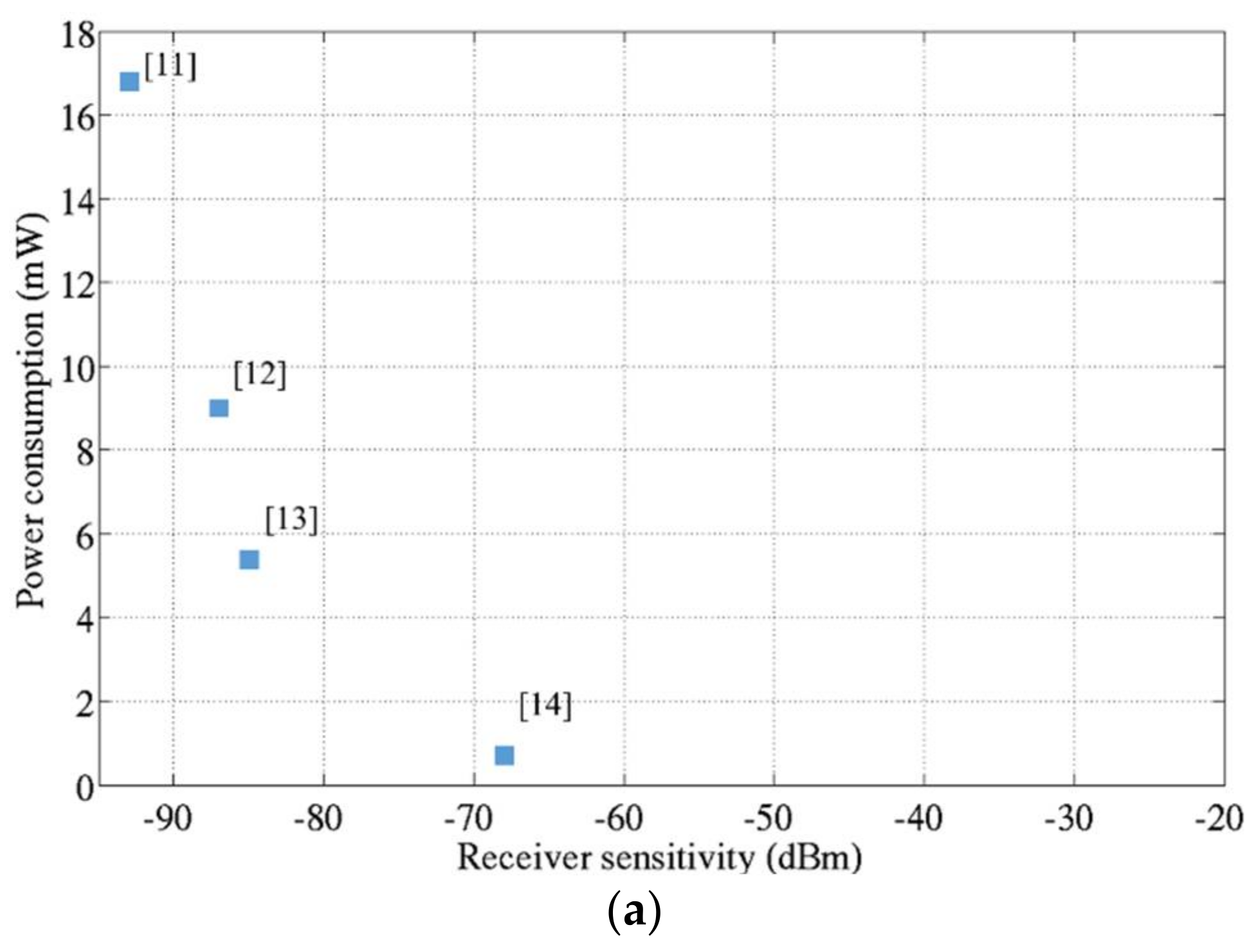
In order to evaluate the reduction on the power consumption of the receiver when its sensitivity is degraded, the performance of receivers available in the literature are shown in Figure 7a. It demonstrates that when the receiver sensitivity is relaxed, the power consumption of the overall receiver can be significantly reduced.
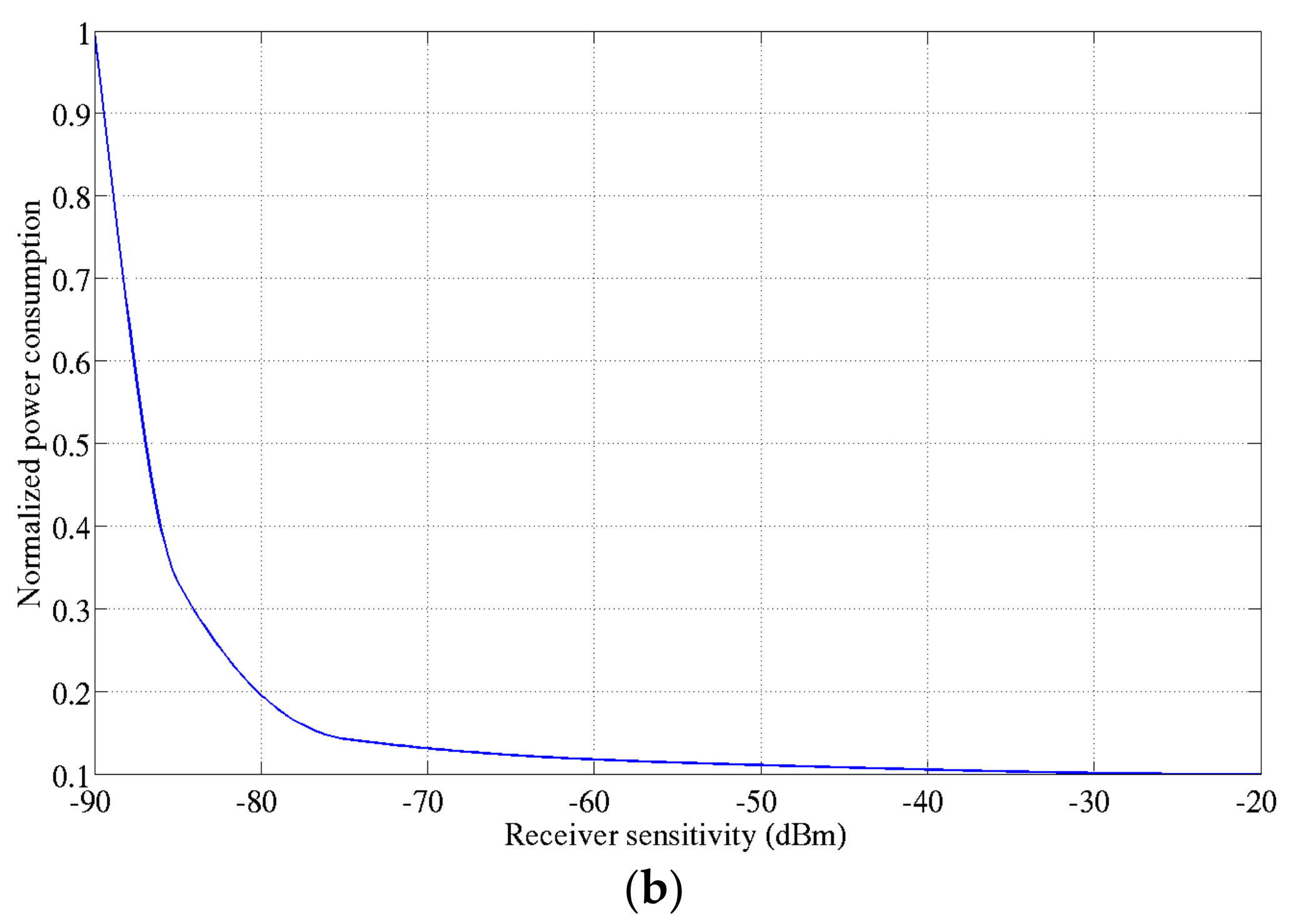
For the best approximation, an asymptotic curve is determined thanks to the receiver’s State of the Art performance. To do so, the power consumption is normalized with respect to the receiver with the minimum sensitivity as plotted in Figure 7b. This model is therefore used in the proposed methodology to define and optimize the operating points of the tunable receiver.

3.4. Optimized Reconfiguration Thresholds

The final approach consists on an optimization of the thresholds using the probability distribution of the received power and the model of the sensitivity versus power consumption. A split of the receiver into several parallel receivers, each one dedicated to a specific range of sensitivity is proposed. The objective is to find the best reconfiguration thresholds in order to optimize the power consumption with a moderate complexity in the system.
Figure 8 shows the split of the PDF of the received signal power at the input of the receiver for each mode of operation.
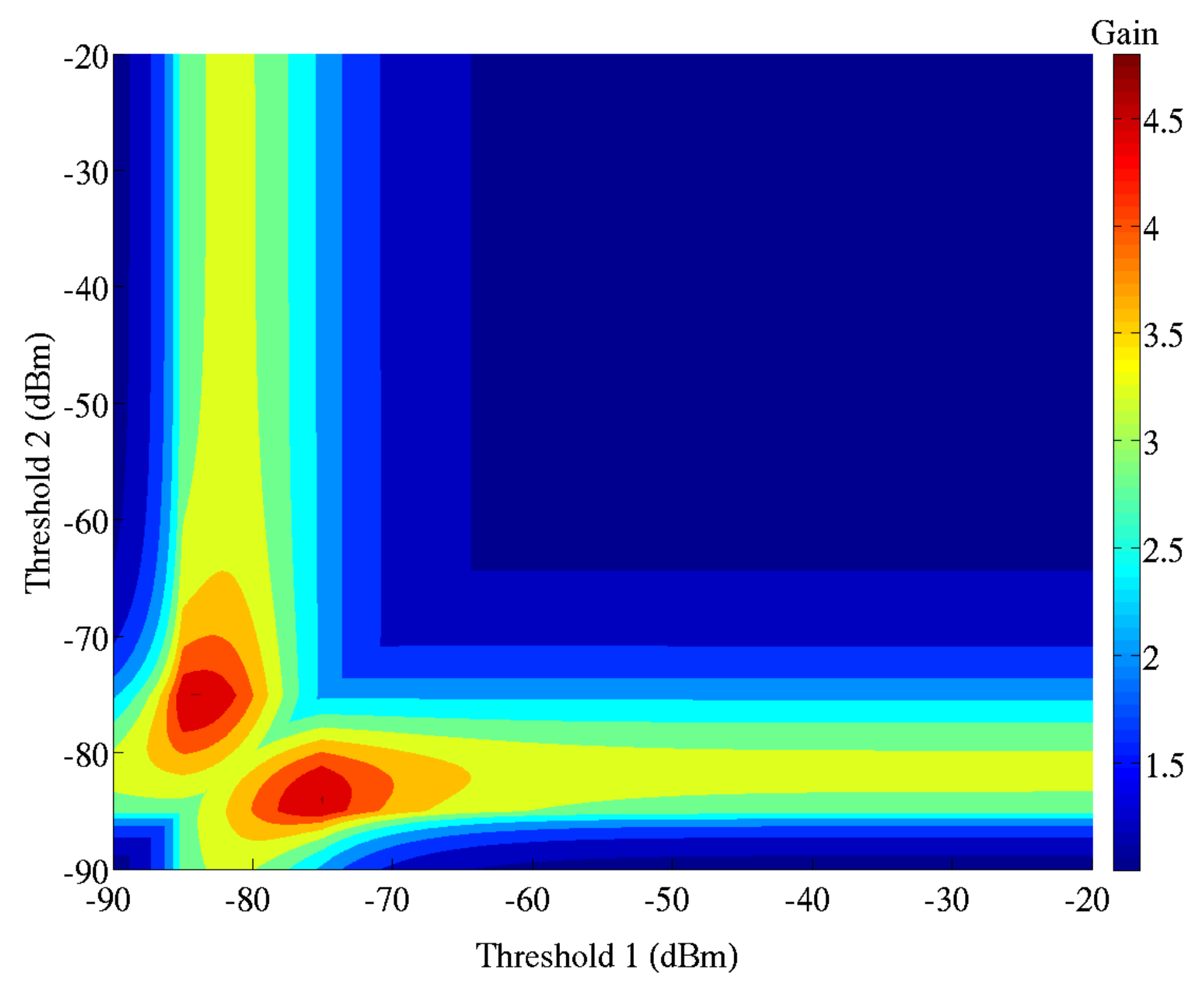
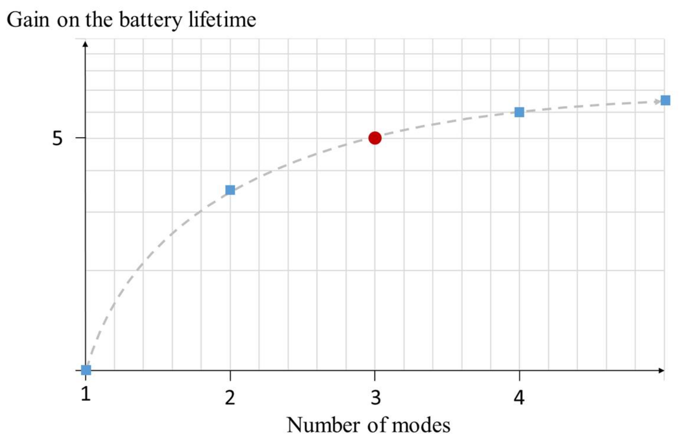
The objective of this study is to find the best configuration of the thresholds (T1 and T2 in a 3 operating point’s receiver) which enables an optimization of the gain on the battery lifetime compared to a traditional receiver. Based on this probability distribution function, different sets of sensitivity thresholds are tested. The gain on the overall power consumption for each set is calculated according to Equation (1).
Gain = t mode 0 . P mode 0 t mode 1 . P mode 1 + + t mode n . P mode n .
With   t mode 0 . P mode 0 = 1 .
where Gain is the gain on the battery lifetime compared to a fixed performance receiver called mode 0, t mode n is the usage time percentage in mode n and P mode n the power consumption normalized with respect to the high performance mode.
The sensitivity thresholds for a 3-modes operation are defined to optimize the overall gain of the power saving. In Figure 9, the gain is represented as a function of the first threshold (T1) and the second threshold (T2). The battery lifetime is extended by a factor of 5 when T1 and T2 are set to −75 and −85 dBm respectively.
The same methodology has been realized for several number of configuration modes. Figure 10 illustrates this gain as a function of the number of modes. The gain on the battery lifetime is significantly increased from a single mode to a 3-modes receiver (red dot on Figure 10). Above, the gain still increases but the relative power savings is significantly reduced. Beside the complexity of implementation, the increase of silicon footprint limits the interest of developing a receiver featuring more than 3 operating modes.
The results of the computation for the proposed 3-modes receiver in terms of sensitivity ranges, percentages of the usage time in each mode and power consumptions are summed up in Table 2.
The power consumption is based on the model depicted on Figure 7b. In order to multiply the battery lifetime of the receiver by a factor of 5, the receiver has to follow the three operating point configurations:
-
The low performance mode has to be designed with a power consumption of 2.2 mW. It will be on this state for 76% of its lifetime.
-
The medium mode has to be designed with a 5.8 mW of power consumption it will be active for 23% of its lifetime.
-
The highest mode is the worst case design, essential to guarantee the QoS but active only 1% of the receiver’s lifetime.
The three optimized operating modes with sensitivity and power consumption are now defined at the receiver point of view. The high performance mode, which addresses the worst case of a sensitivity of −90 dBm, is the most available design in the State of the Art and in the industry (as the ATMEL module presented in Section 2.2, for instance). From the results of Table 2, the system analysis demonstrates that the proposed receiver is most of the time (76% of its lifetime) at low power mode operating point.
This approach of the Ultra Low Power (ULP) receiver needs to be validated at a silicon point of view.
As illustrated in Figure 11, the focus of next section is to determine the specification of the receiver and of the LNA at this level of performance. In fact, as the first element of the receiver chain, the LNA limits the receiver in terms of sensitivity and is therefore a good candidate to be optimized at this sensitivity level.

3.5. Design Specifications

The LNA performance (Noise Figure NF, Voltage Gain Gv) are determined with Friis Equations and performance of the State of The Art blocks of the chain. In fact, the mixer performance is based on the mixer proposed in [15]. The baseband noise figure and gain performance chosen are based on the Variable Gain Amplifier (VGA) proposed in [16]. The power consumption of the LNA is based on the repartition of the power consumption in a receiver (Figure 2b) and on the receiver power consumption model (Figure 7b).
Table 3 presents the targeted design specifications of the low performance receiver based on the system analysis.
Because the power consumption of the LNA aimed with this study is only given based on the State of The Art power consumption repartition in a receiver, it is essential to validate the feasibility of this power reduction with IC measurements.
Therefore, a Figure of Merit (FoM) defined in Equation (2) is chosen in order to evaluate the performance and power consumption of the LNA. The calculation of the FoM based on performance of Table 3 gives 23. As it will be shown later with the State of the Art of ULP LNA, this FoM of 23 is quite challenging as it is over the FoM of the best LNA designs available in the literature.
FoM I   = 20 log ( Gv ( lin ) . BW ( GHz ) Pdc   ( mW ) . ( NF ( lin ) 1 ) )
where BW is the bandwith in GHz of the LNA.
The LNA targeted performance have been calculated for the low power receiver. Next section proposes to design an ULP LNA aiming this theoretical FoM in order to validate the system level approach at a silicon point of view.

4. FD-SOI ULP LNA Design for IoT Applications

4.1. LNA Topology

Reducing the form factor to propose small chip area RFIC designs is essential. To address this purpose, inductor based circuits are now replaced by inductorless RF blocks. Among the tough challenge in the design of inductorless ULP LNA design, is the synthesis of a wideband input matching.
There are two possibilities to achieve a 50 Ω-input impedance inductorless LNA designs. First, a Common Source with resistive feedback technique [17] could be used but this topology degrades the output impedance and requires a large power for sufficient voltage gain. The other solution is to design a Common Gate topology. This configuration offers the possibility of an easy input matching through the transconductance (gm) of the input transistor. For these reasons, a Common Gate architecture is selected in this work. In order to guarantee a large voltage gain, a gm-boost is added to the common gate architecture [18].
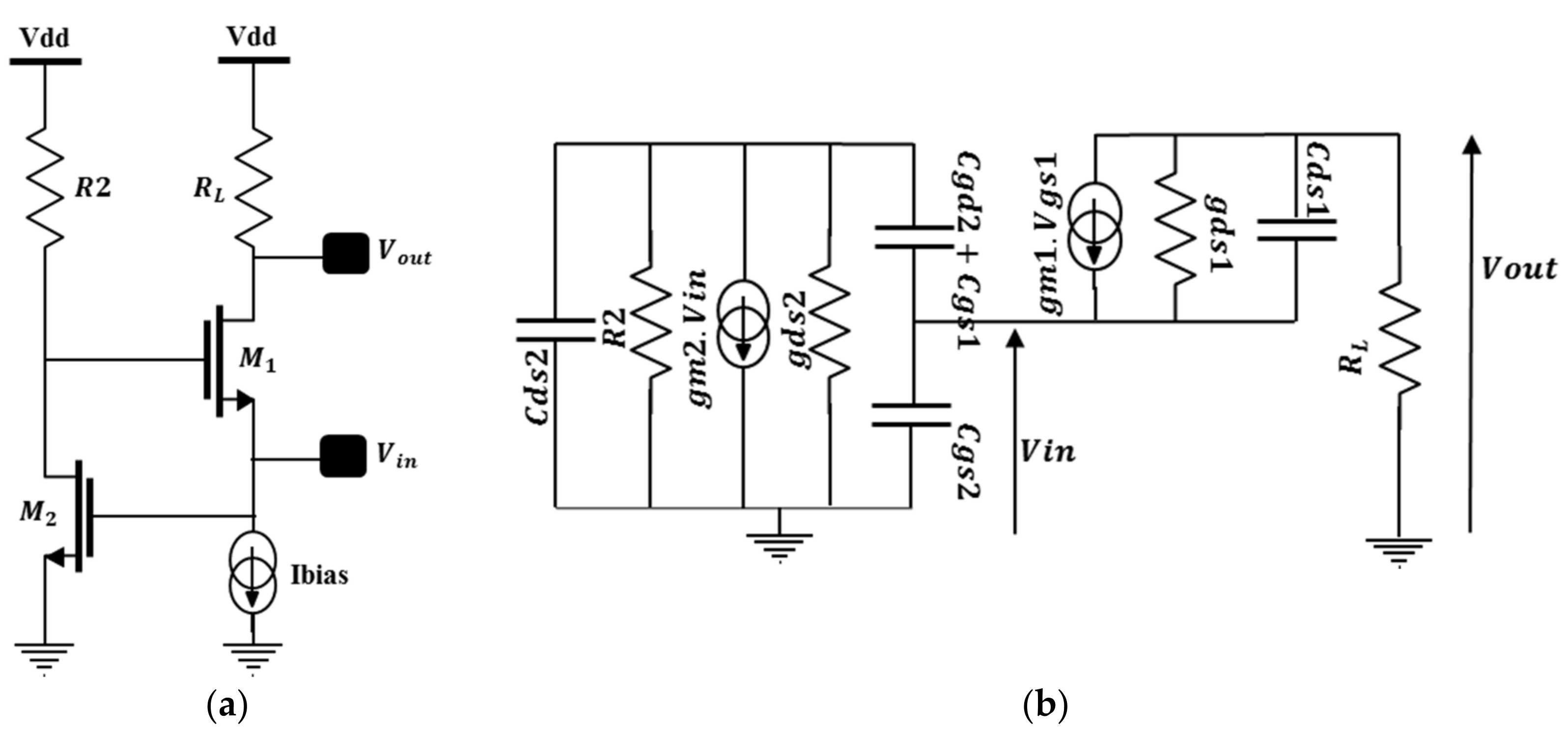
The topology of the proposed LNA and its simplified small signal model are depicted in Figure 12a,b, respectively. M1 and RL feature the common gate amplifier which is enhanced by the additional common source gm-boost M2-R2. The RF signal is simultaneously applied to the source and the gate of M1 through (M2-R2). This configuration enables an increase of its gate to source voltage (Vgs) and thus enhances the available gain. This architecture offers the possibility to reach large gain, good input matching and reasonable noise figure under low power constraints.
To improve the performance with this topology, which has been already studied in the literature [12,19], an exploration of the back gate biasing to further reduce the voltage supply and the power consumption is proposed.
The equivalent voltage gain GvLNA, the input impedance ZinLNA and the Noise Figure NFLNA of this architecture are given in Equations (3)–(5) respectively.
Gv LNA   =   gm 1 .   ( 1 + gm 2 . R 2 + C ds 2 . R 2 . j ω ) 1 + C ds 2 . R 2 . j ω + ( C gd 2 + C gs 1 ) . R 2 . j ω + gds 1 + C ds 1 . j ω gds 1 + 1 R 1 + C ds 1 . j ω ;
Zin LNA   = 1 + C ds 2 . R 2 . j ω + C 12 . R 2 . j ω gm 1 ( 1 + gm 2 R 2 + C ds 2 R 2 j ω ) C gs 2 j ω C ds 2 C gs 2 R 2 ω 2 + C 12 j ω + gm 2 C 12 R 2 j ω C ds 2 C 12 R 2 ω 2 + C gs 2 C 12 R 2 ω ²   ;     With   C 12 = C gd 2 + C gs 1 .
NF LNA = 1 + 2 3 + 2 3 . gm 2 . R 2 2 . gm 1 + 4 . R 2 gm 1 ( 1 + gm 1 . R s ) ² R S . ( 1 + gm 2 . R 2 ) 2 . gm 1 .
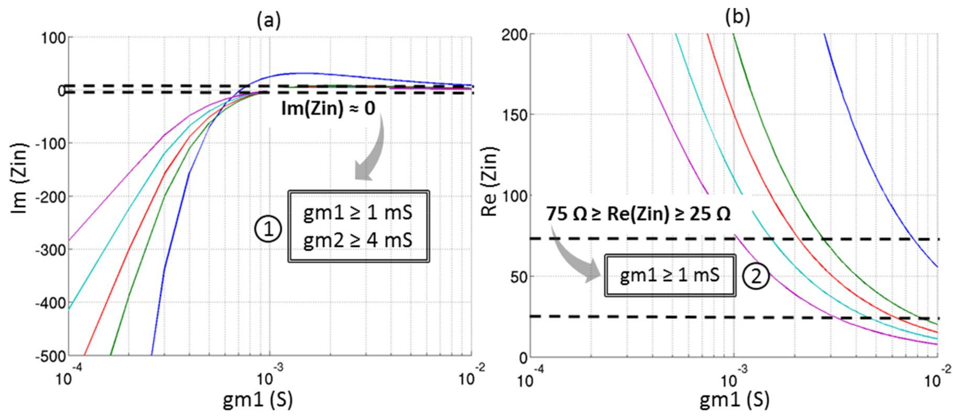
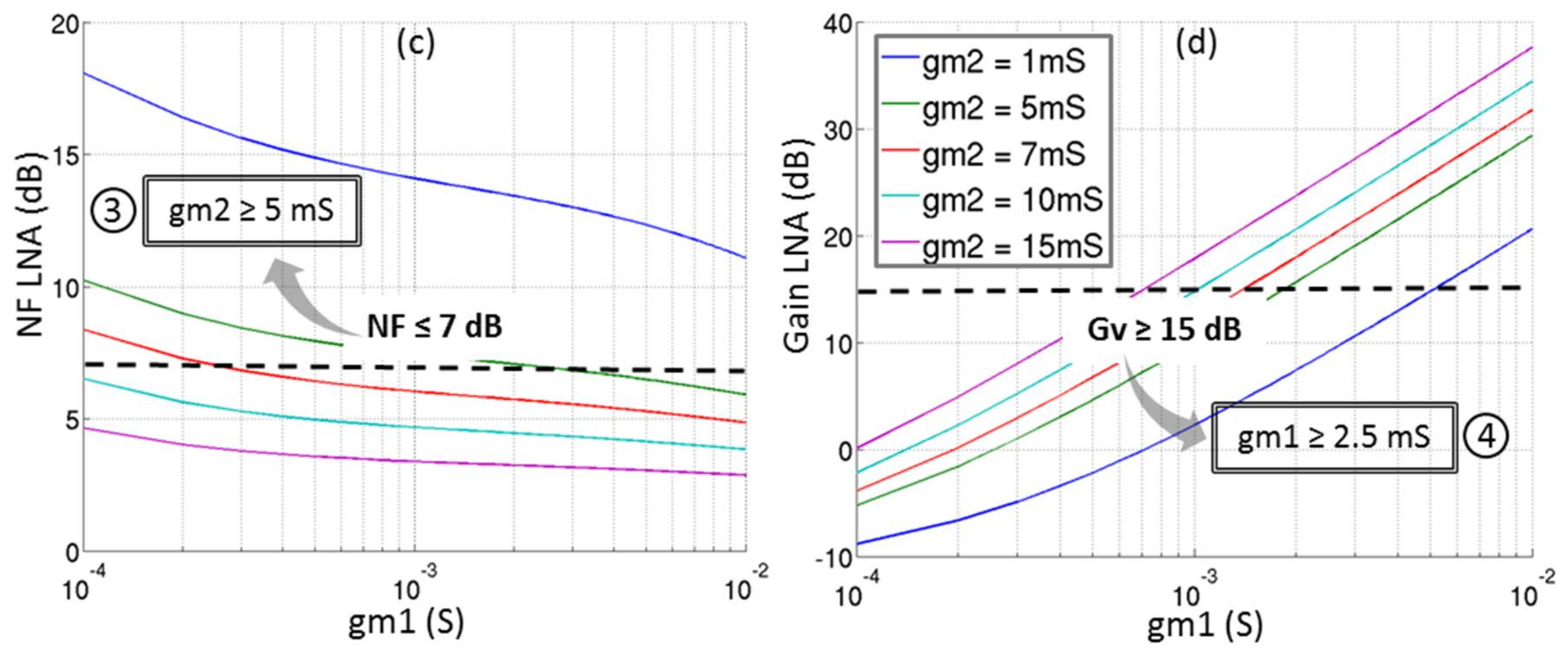
The behavior of the input impedance, the noise figure and the voltage gain described in Equations (3)–(5) are depicted in Figure 13 for different couples of (gm1, gm2). The input matching is considered as acceptable—i.e., real part of Zin between 25 Ω and 75 Ω and imaginary part of Zin close to 0 which gives a S11 under −10 dB. The conditions on (gm1, gm2) which fit the requirements of Table 3 in terms of noise figure (≥7 dB) and voltage gain (≥15 dB) are also illustrated.
In order to optimize the power consumption, the minimum of gm1 and gm2 respecting the conditions ①, ②, ③, and ④ are determined:
-
gm1 = 2.5 mS;
-
gm2 = 5 mS.
Therefore, the widths of the transistors have been chosen along with the DC biasing in order to obtain the needed (gm1, gm2) for the minimum power consumption. Active transistors of the LNA (M1 and M2) have minimum gate length to achieve a maximum bandwidth at a minimum power consumption.
The following part proposes a succinct description of the FD-SOI transistor and the body biasing effects in order to evaluate the benefits on the proposed ULP LNA.

4.2. Body Biasing

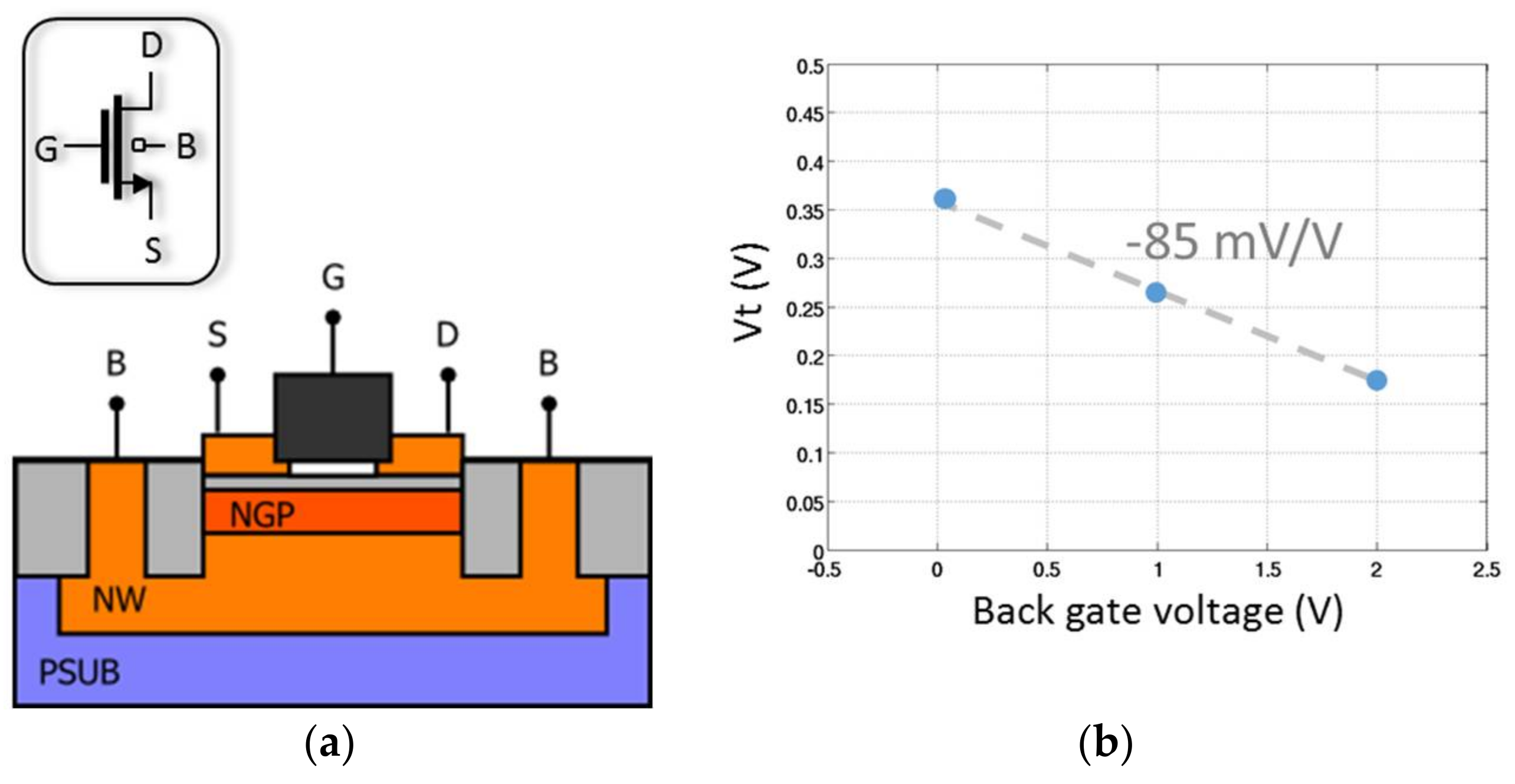
Figure 14 illustrates the cross section of an nLVT FD-SOI transistors. As depicted, its channel is isolated from the substrate. Therefore, there is no junction diodes as bulk-drain and bulk-source and body biasing is thus possible. This body biasing enables a reduction of its threshold voltage with a slope of −85 mV/V (see Figure 14b).
The large variation range on the threshold voltage of the transistor enables new DC operating points on the LNA. In fact, to maintain the saturation of the transistors, the following conditions on the transistor operating point have to be respected:
-
Vgs ≥ Vt;
-
Vds ≥ Vgs−Vt.
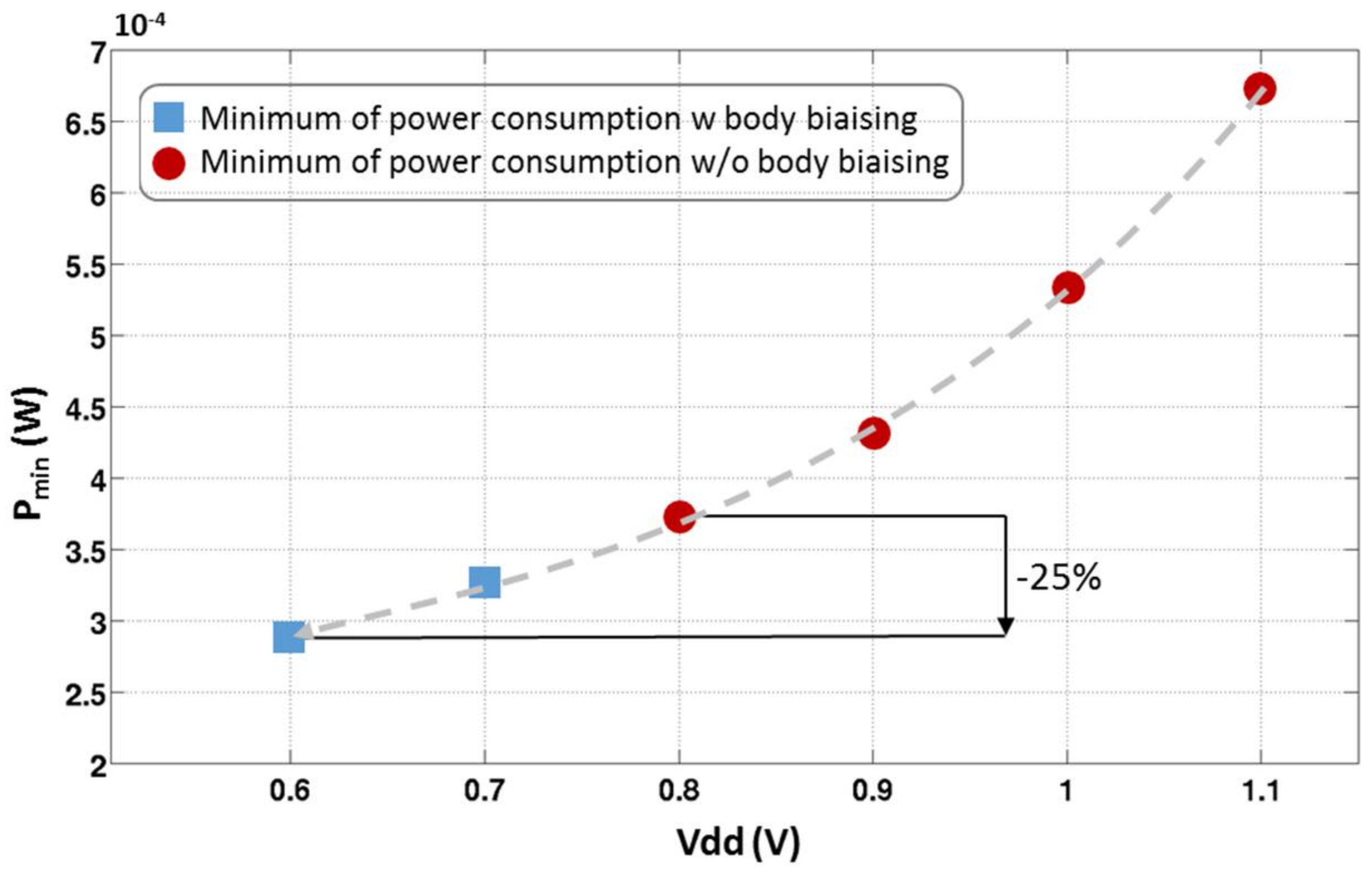
Figure 15 shows the minimum of power consumption (several W1, W2, and Ibias) reached for each power supply respecting the design specifications (GvLNA = 15 dB, NFLNA ≤ 7 dB, and S11 ≤ −10 dB). The dots represent the solutions without any back gate biasing. The minimum of power consumption in that case is reached for Vdd = 0.8 V. Beyond this power supply, there is no solution for a correct saturation of the transistors. The power consumption of the LNA at this operating point is 380 µW. This design solution gives a FoM of 25.3 with is over the theoretical FoM aimed in Section 4. Even without using the body biasing of the FD-SOI technology, this technology enables good design performance making it one of the best FoM of State of the Art LNA.
However, this work shows a way to push further the limitation on the saturation of the transistor thanks to the possibility of lowering the threshold voltage of the transistor with the body biasing. Therefore, when a voltage is applied on the body of the transistor, more design solutions with the same performance are available for a lower power consumption.
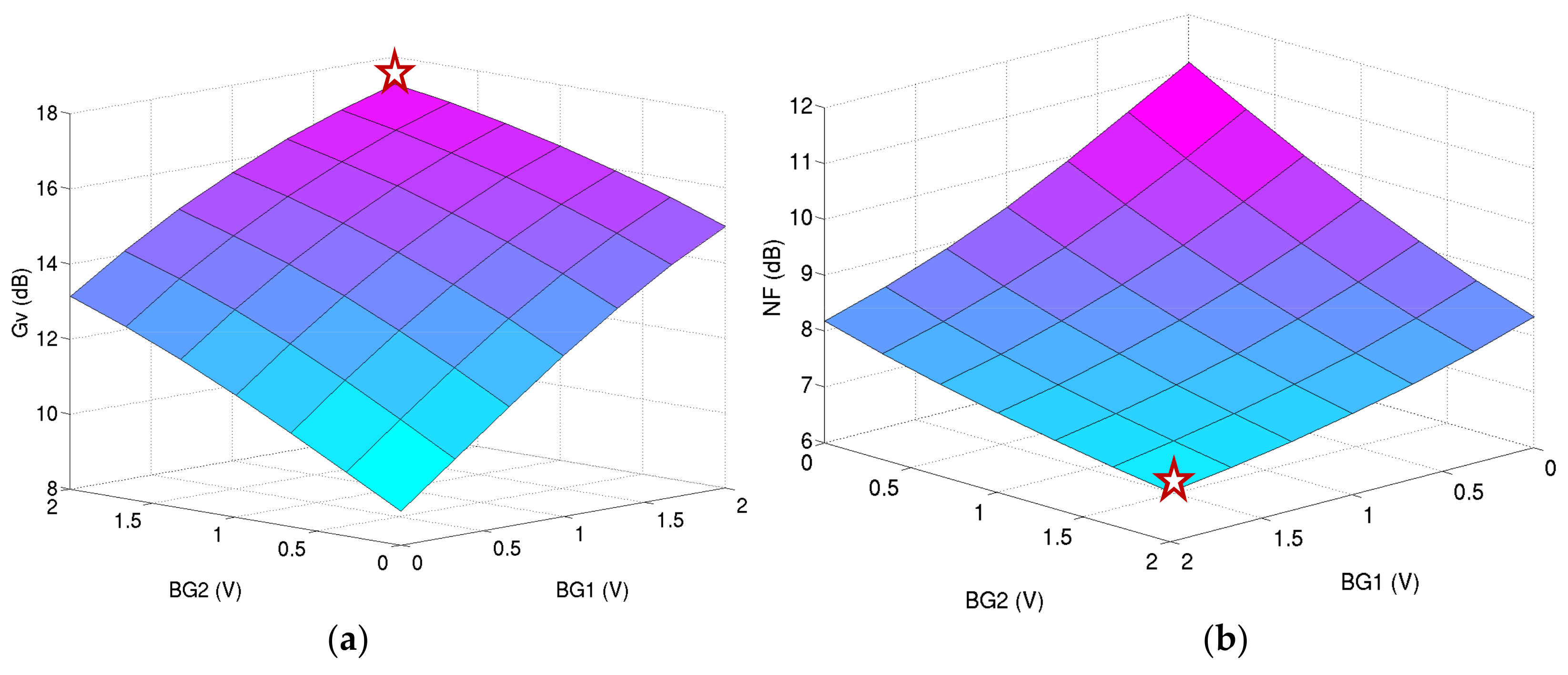
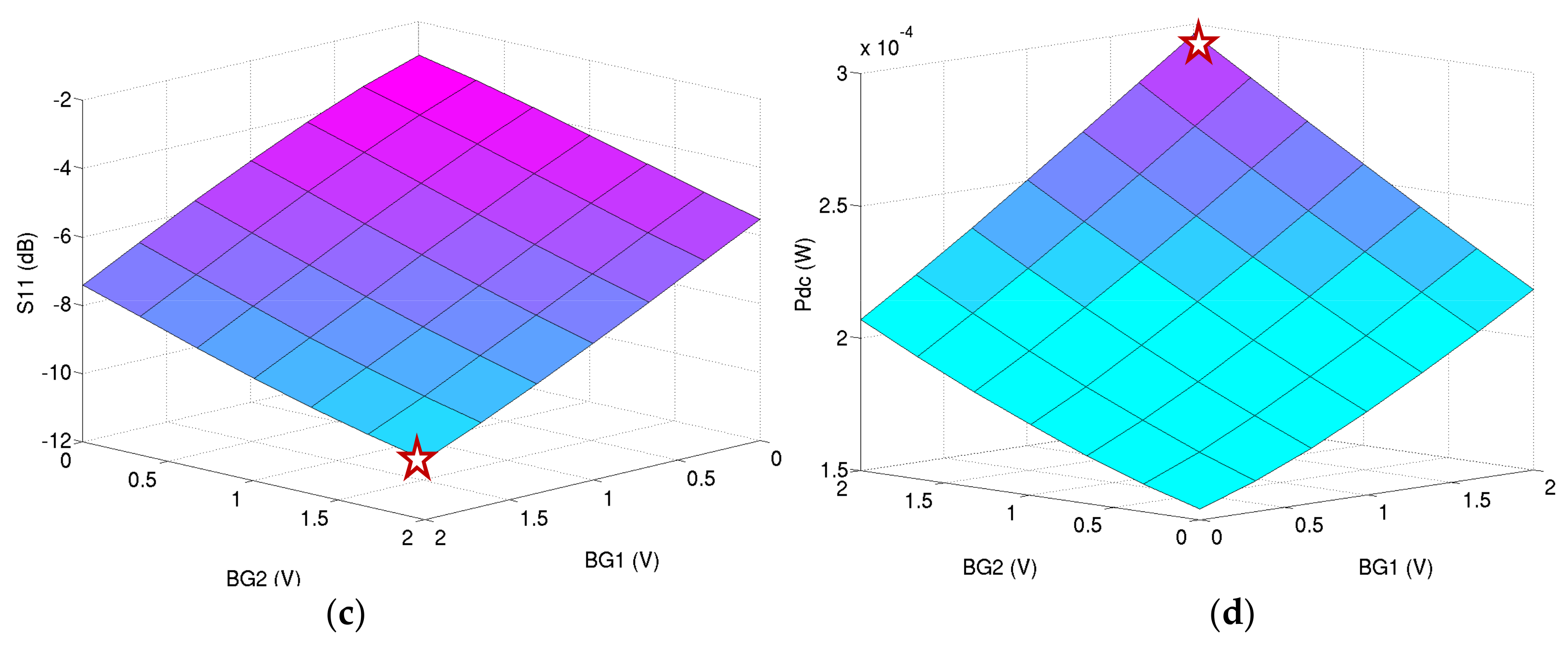
Figure 16 depicts the simulation results for the ULP LNA at a 0.6 V power supply for several voltages on back gate of M1 and M2. It confirms that the performance cannot be maintained without the body biasing at this power supply.
The chosen operating point (plotted red star on Figure 16) is the lowest power consumption providing the correct performance:
-
BG1 = 2 V;
-
BG2 = 2 V; and
-
Vdd = 0.6 V.
This operating point gives the simulated performance at 2.4 GHz:
-
S11 = −10.5 dB;
-
Gv = 17.5 dB;
-
NF = 6.9 dB; and
-
Pdc = 300 µW.
By using the body biasing, the threshold voltage of the transistors is decreased and the power supply voltage can thus be reduced to 0.6 V with a back gate voltage of +2 V. More than 25% of the power consumption on the LNA can be saved.

4.3. PVT Degradation Evaluation

As the technology is decreasing to deep submicron processes, the circuit process, voltages and temperature variations can degrade the RF performance of the LNA. The system analysis proposed in Section 3 validates the needs of a sensitivity of −75 dBm for the low power mode. This threshold has to be guaranteed even with Process Voltage Temperature (PVT) deviations.
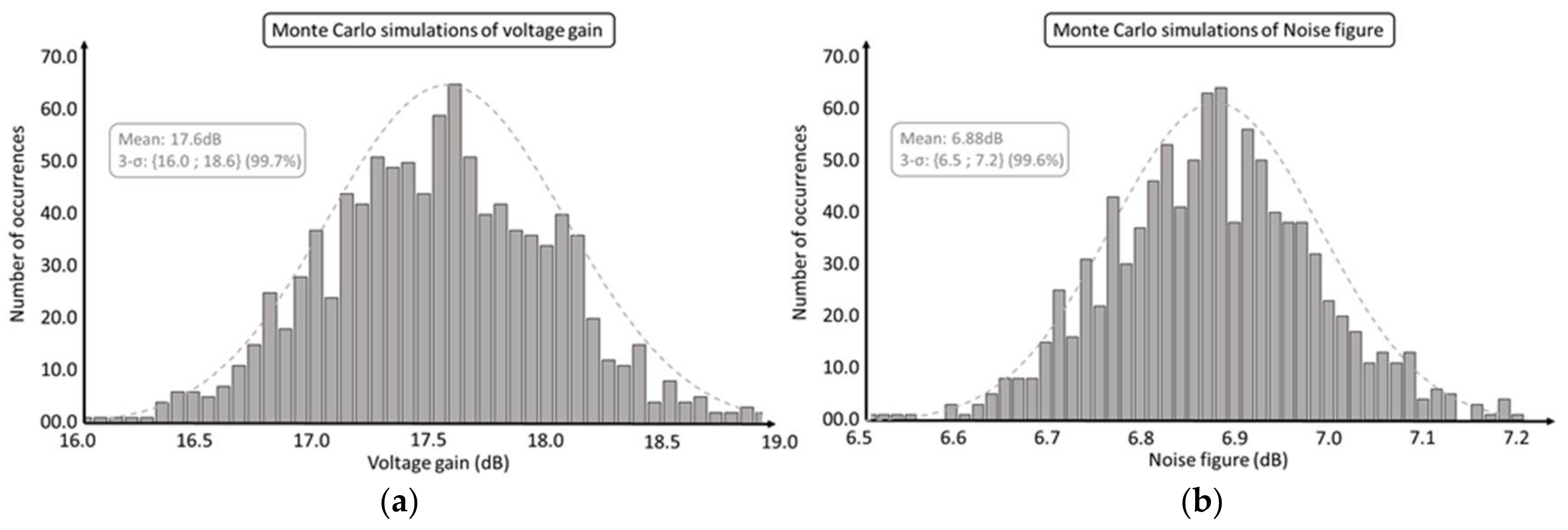
Figure 17 shows the Monte Carlo simulations performed for 1000 occurrences and the extraction of the LNA’s voltage gain and noise figure at 2.4 GHz.
The performance of the LNA at the minimum and maximum of 3-σ Monte Carlo simulations results have been introduced to the system analysis described in Section 3 in order to evaluate the impact of the PVT variation of the LNA on the receiver’s sensitivity (others blocks of the chain have been considered at fixed performance).
Table 4 presents the worst and best 3-σ Monte Carlo simulations noise figure and voltage gain of the LNA and their impact on the sensitivity of the receiver. The results shows a delta of 1.5 dB on the sensitivity of the receiver. Even for the worst PVT performance deviation, the sensitivity threshold −75 dBm is guaranteed with the design of this LNA.

5. Integrated Circuit (IC) Implementation and Measurement Results

5.1. ULP LNA Mesurement Results

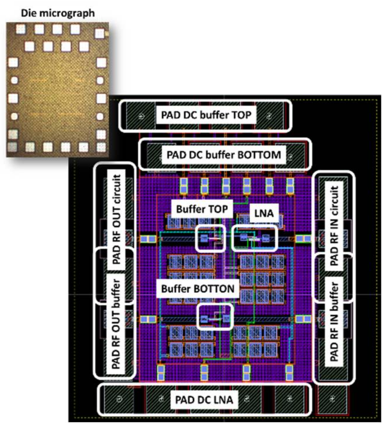
The ULP LNA circuit has been implemented in Ultra-Thin Body and Buried oxide (UTBB) FD-SOI 28 nm ST-Microelectronics technology. Figure 18 shows the die micrograph and the layout view of the chip. The complete chip has an area of 0.5 mm2 and the LNA core is only 0.0015 mm2. The ULP LNA is followed by a buffer added only for test facilities (output matching). The S-parameters and characteristics of this buffer are de-embedded from the proposed measurement results.
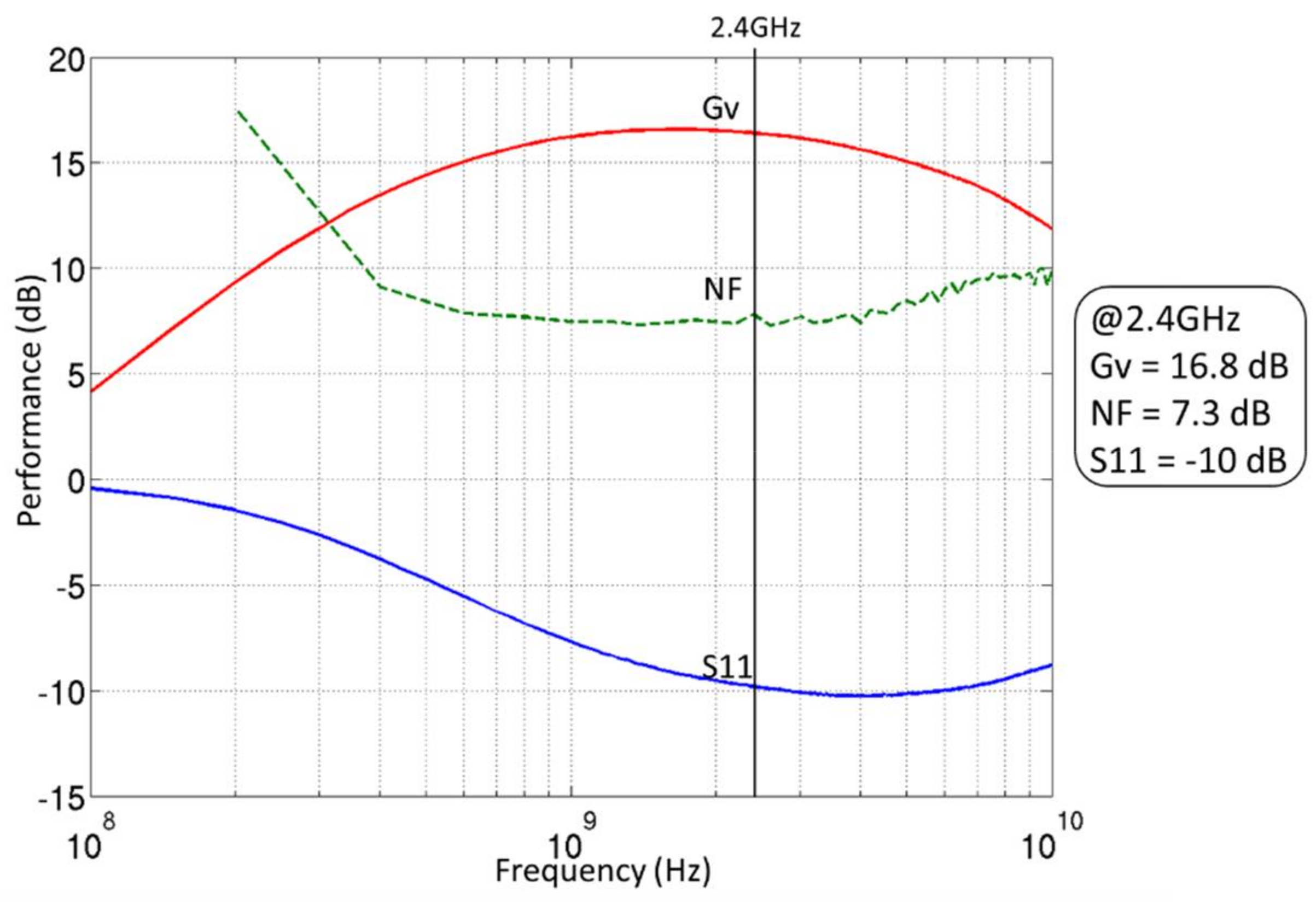
Results of the measured voltage gain (Gv), noise figure (NF), and input matching (S11) for the optimized ULP mode are plotted in Figure 19. The proposed LNA achieves, at 2.4 GHz, a 16.8 dB voltage gain and a 7.3 dB noise figure for a power consumption of 300 µW under 0.6 V of power supply. Such performance are not achievable without the use of the back biasing (in this case +2 V on both transistors) which validates the benefits of the FD-SOI technology to decrease the power consumption of a block.
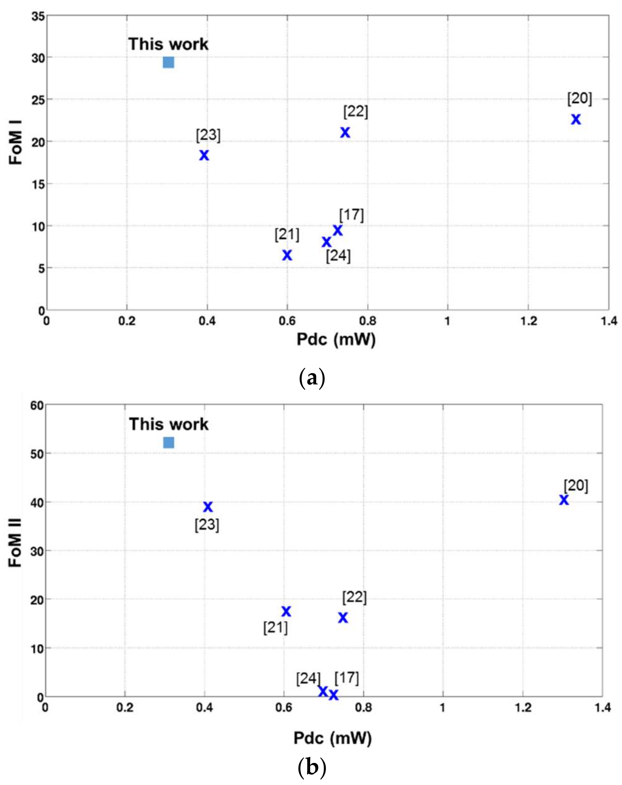
The performance of the LNA are summarized and compared with the State Of the Art ULP LNAs in Table 5. In order to compare the circuits, two FoMs are used and defined in Equations (2) and (6).
FoM II   = 20 log ( Gv ( lin ) . BW ( GHz ) . IIP 3 ( mW ) Pdc   ( mW ) . ( NF ( lin ) 1 ) . A ( mm 2 ) )
where BW is the bandwith in GHz of the LNA and A the area in mm2.
The proposed LNA achieves a very low power consumption with comparable State Of the Art LNAs performance, leading to highest FoM I and FoM II as depicted in Figure 20. The results and State of the Art LNAs performance are detailed in Table 5.

5.2. Gain on the Battery Lifetime with the Proposed LNA

This section evaluates the impact of the ULP LNA performance results on the gain of the battery lifetime of the whole system through the same system analysis presented in Section 3. Table 6 shows the gain reached in the theoretical case with the FoM of the LNA of 23 and with the measured FoM of 29.3. The other blocks of the chain are considered impacted on the same way than the LNA due to the technology performance.
The body biasing used to lower the power consumption of the LNA enables a better gain (6.7 instead of 5.1) than expected with the system analysis. Even if the validation of such tunable receiver has to be done at silicon level on all the blocks, the proof of concept has been validated on the LNA and the approach demonstrates the feasibility through the proposed ULP LNA.

6. Conclusions

A new method to increase the battery lifetime of a receiver is proposed. Adding tunability with discrete optimized operating modes is exploited in this study as a way to decrease the power consumption of the communicating node. In order to be fully efficient, a judicious and proper choice in these operating points needs to be done. This study shows a smart system analysis to choose these reconfiguration levels. Furthermore, the study is extended to the first element of the receiver: the LNA where a described methodology is proposed to define the targeted performance. The ULP LNA has been implemented in FD-SOI technology and the benefits of this technology to decrease the power consumption has been demonstrated. Finally, the approach enables an extension of the battery lifetime of a communicating node by a factor of 6.7 with the measured LNA. To the knowledge of the author, the proposed inductorless ULP LNA exhibits the best Figure of Merit (FoM) of the State of the Art reported in the literature so far.

Acknowledgments

The authors would like to thank Magali De Matos (IMS Bordeaux) for her availability and her help during the measurements of the Ultra Low Power (ULP) Low Noise Amplifier (LNA).

Author Contributions

Frédéric Hameau and Patrick Audebert are both supervisors of the PhD student Jennifer Zaini-Desevedavy. Jennifer Zaini-Desevedavy and Frédéric Hameau conceived and designed the circuit; Jennifer Zaini-Desevedavy and Patrick Audebert analyzed the body biasing effect on the circuit. Thierry Taris and Dominique Morche are thesis director and co-director of Jennifer Zaini-Desevedavy. They contributed on analyzing the data and wrote the paper with Jennifer Zaini-Desevedavy.

Conflicts of Interest

The authors declare no conflict of interest.

References

  1. Take the World with You. Available online: https://www.ericsson.com/assets/local/investors/documents/financial-reports-and-filings/annual-reports/ericsson_ar_2010_en.pdf (accessed on 13 December 2017).
  2. Bachir, A.; Dohler, M.; Watteyne, T.; Leung, K.K. MAC Essentials for Wireless Sensor Networks. IEEE Commun. Surv. Tutor. 2010, 12, 222–248. [Google Scholar] [CrossRef]
  3. Raja, M.K.; Chen, X.; Lei, Y.D.; Bin, Z.; Yeung, B.C.; Xiaojun, Y. A 18 mW Tx, 22 mW Rx transceiver for 2.45 GHz IEEE 802.15.4 WPAN in 0.18-µm CMOS. In Proceedings of the 2010 IEEE Asian Solid State Circuits Conference (A-SSCC), Beijing, China, 8–10 November 2010; pp. 1–4. [Google Scholar]
  4. Pletcher, N.M.; Gambini, S.; Rabaey, J. A 52 µW Wake-Up Receiver with −72 dBm Sensitivity Using an Uncertain-IF Architecture. IEEE J. Solid State Circuits 2009, 44, 269–280. [Google Scholar] [CrossRef]
  5. Lanzisera, S.; Mehta, A.M.; Pister, K.S.J. Reducing Average Power in Wireless Sensor Networks through Data Rate Adaptation. In Proceedings of the 2009 IEEE International Conference on Communications, Dresden, Germany, 14–18 June 2009; pp. 1–6. [Google Scholar]
  6. Dwivedi, S.; Amrutur, B.; Bhat, N. Power Scalable Radio Receiver Design Based on Signal and Interference Condition. J. Low Power Electron. Appl. 2012, 2, 242–264. [Google Scholar] [CrossRef]
  7. Oguz, A.; Morche, D.; Dehollaini, C. Adaptive power reconfigurability for decreasing power dissipation of wireless personal area network receivers. In Proceedings of the 2011 IEEE International Symposium on Circuits and Systems (ISCAS), Rio de Janeiro, Brazil, 15–18 May 2011; pp. 1900–1903. [Google Scholar]
  8. Lolis, L.; de Souza, M.; Zambon, L.B.; Mariano, A. Impact of a fully reconfigurable LNA on an RF front-end: A system level analysis. In Proceedings of the 2014 21st IEEE International Conference on Electronics, Circuits and Systems (ICECS), Marseille, France, 7–10 December 2014; pp. 662–665. [Google Scholar]
  9. Banerjee, D.; Muldrey, B.; Wang, X.; Sen, S.; Chatterjee, A. Self-Learning RF Receiver Systems: Process Aware Real-Time Adaptation to Channel Conditions for Low Power Operation. IEEE Trans. Circuits Syst. Regul. Pap. 2017, 64, 195–207. [Google Scholar] [CrossRef]
  10. Zaini, J.; Hameau, F.; Taris, T.; Morche, D.; Tran, L.Q.V.; Audebert, P. Channel aware receiver front end for low power 2.4 GHz Wireless Sensor Network: A system level analysis. In Proceedings of the 2016 14th IEEE International New Circuits and Systems Conference (NEWCAS), Vancouver, BC, Canada, 26–29 June 2016; pp. 1–4. [Google Scholar]
  11. Retz, G.; Shanan, H.; Mulvaney, K.; O’Mahony, S.; Chanca, M.; Crowley, P.; Billon, C.; Khan, K.; Quinlan, P. A highly integrated low-power 2.4 GHz transceiver using a direct-conversion diversity receiver in 0.18 µm CMOS for IEEE802.15.4 WPAN. In Proceedings of the IEEE International Solid-State Circuits Conference—Digest of Technical Papers, ISSCC 2009, San Francisco, CA, USA, 8–12 February 2009; pp. 414–415. [Google Scholar]
  12. Kwon, Y.-I.; Park, T.J.; Cho, K.-S.; Lee, H.-Y. A 9 mW Highly-Digitized 802.15.4 Receiver Using Bandpass ADC and IF Level Detection. IEEE Microw. Wirel. Compon. Lett. 2008, 18, 824–826. [Google Scholar] [CrossRef]
  13. Camus, M.; Butaye, B.; Garcia, L.; Sie, M.; Pellat, B.; Parra, T. A 5.4 mW 0.07 mm2 2.4 GHz Front-End Receiver in 90 nm CMOS for IEEE 802.15.4 WPAN. In Proceedings of the IEEE International Solid-State Circuits Conference—Digest of Technical Papers, ISSCC 2008, San Francisco, CA, USA, 3–7 February 2008; pp. 368–620. [Google Scholar]
  14. Perumana, B.G.; Mukhopadhyay, R.; Chakraborty, S.; Lee, C.-H.; Laskar, J. A Low-Power Fully Monolithic Subthreshold CMOS Receiver with Integrated LO Generation for 2.4 GHz Wireless PAN Applications. IEEE J. Solid State Circuits 2008, 43, 2229–2238. [Google Scholar] [CrossRef]
  15. Lont, M.; Milosevic, D.; Dolmans, G.; van Roermund, A.H.M. Mixer-First FSK Receiver with Automatic Frequency Control for Body Area Networks. IEEE Trans. Circuits Syst. Regul. Pap. 2013, 60, 2051–2063. [Google Scholar] [CrossRef]
  16. Elwan, H.; Tekin, A.; Pedrotti, K. A Differential-Ramp Based 65 dB-Linear VGA Technique in 65 nm CMOS. IEEE J. Solid State Circuits 2009, 44, 2503–2514. [Google Scholar] [CrossRef]
  17. Wang, S.B.T.; Niknejad, A.M.; Brodersen, R.W. Design of a Sub-mW 960-MHz UWB CMOS LNA. IEEE J. Solid State Circuits 2006, 41, 2449–2456. [Google Scholar] [CrossRef]
  18. Belmas, F.; Hameau, F.; Fournier, J. A Low Power Inductorless LNA with Double Enhancement in 130 nm CMOS. IEEE J. Solid State Circuits 2012, 47, 1094–1103. [Google Scholar] [CrossRef]
  19. Kim, J.; Hoyos, S.; Silva-Martinez, J. Wideband Common-Gate CMOS LNA Employing Dual Negative Feedback with Simultaneous Noise, Gain, and Bandwidth Optimization. IEEE Trans. Microw. Theory Tech. 2010, 58, 2340–2351. [Google Scholar] [CrossRef]
  20. Belmas, F.; Hameau, F.; Fournier, J. A 1.3 mW 20 dB gain low power inductorless LNA with 4 dB Noise Figure for 2.45 GHz ISM band. In Proceedings of the 2011 IEEE Radio Frequency Integrated Circuits Symposium (RFIC), Baltimore, Maryland, 5–7 June 2011; pp. 1–4. [Google Scholar]
  21. Li, Z.; Wang, Z.; Zhang, M.; Chen, L.; Wu, C.; Wang, Z. A 2.4 GHz Ultra-Low-Power Current-Reuse CG-LNA with Active-Boosting Technique. IEEE Microw. Wirel. Compon. Lett. 2014, 24, 348–350. [Google Scholar] [CrossRef]
  22. Parvizi, M.; Allidina, K.; El-Gamal, M.N. A Sub-mW, Ultra-Low-Voltage, Wideband Low-Noise Amplifier Design Technique. IEEE Trans. Very Large Scale Integr. VLSI Syst. 2015, 23, 1111–1122. [Google Scholar] [CrossRef]
  23. Parvizi, M.; Allidina, K.; El-Gamal, M.N. An Ultra-Low-Power Wideband Inductorless CMOS LNA with Tunable Active Shunt-Feedback. IEEE Trans. Microw. Theory Tech. 2016, 64, 1843–1853. [Google Scholar] [CrossRef]
  24. Fiorelli, R.; Silveira, F.; Peralı, E. MOST Moderate—Weak-Inversion Region as the Optimum Design Zone for CMOS 2.4-GHz CS-LNAs. IEEE Trans. Microw. Theory Tech. 2014, 62, 556–566. [Google Scholar] [CrossRef]
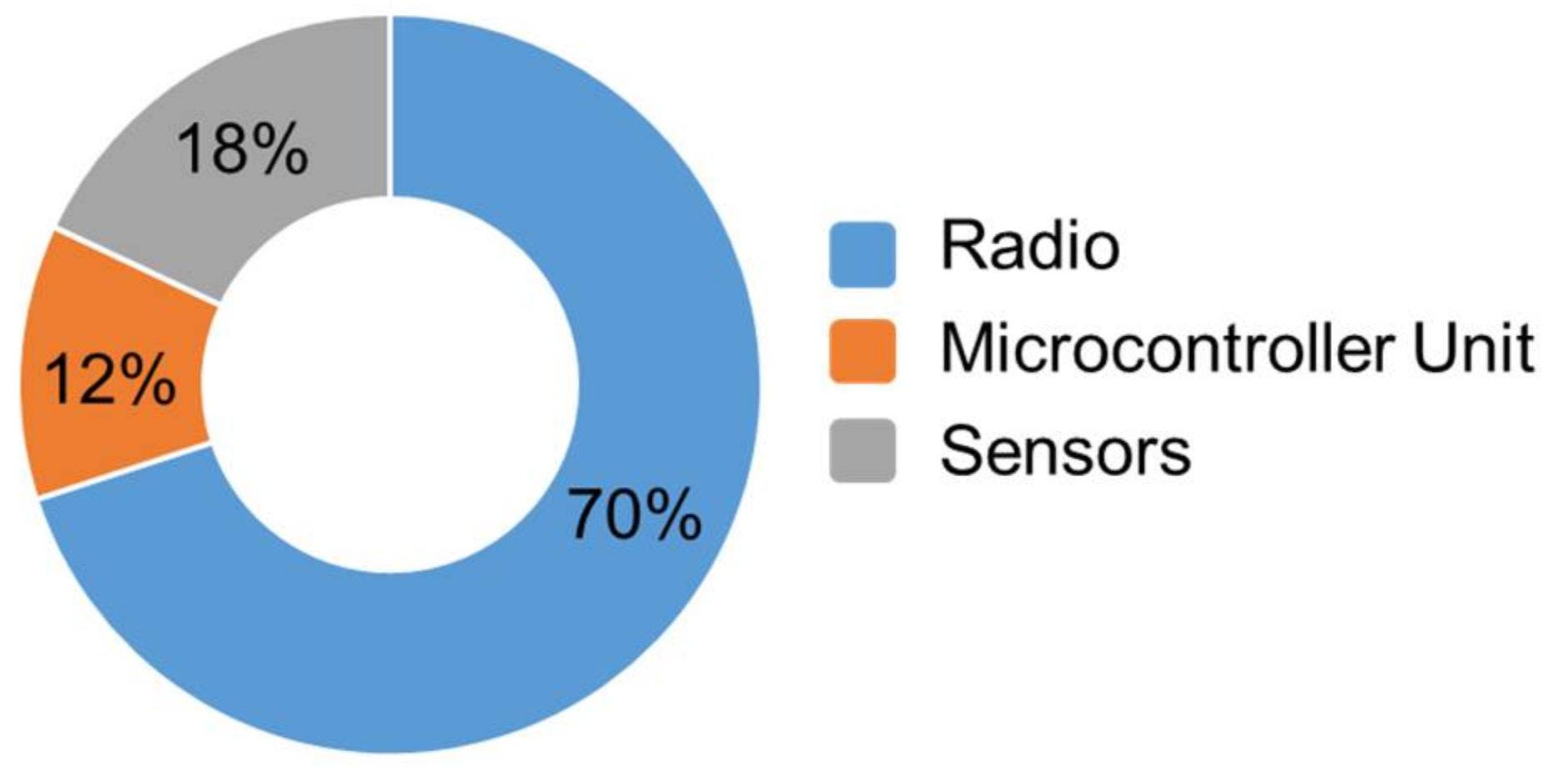
Figure 1. Repartition of the power consumption in a wireless sensor node [2].
Jlpea 08 00010 g001
Figure 2. Repartition of the power consumption: (a) in the transmitter and (b) in the receiver [3].
Jlpea 08 00010 g002
Figure 3. Adaptive Receiver Illustration.
Jlpea 08 00010 g003
Figure 4. Illustration of the proposed tunable receiver.
Jlpea 08 00010 g004
Figure 5. (a) Selection of the receiver operating mode during the synchronization preamble and (b) Illustration of intra frame 3-levels reconfiguration receiver.
Jlpea 08 00010 g005
Figure 6. Probability distribution function (PDF) of the received power signal at the input of the receiver [10].
Jlpea 08 00010 g006
Figure 7. Power consumption versus the receiver sensitivity: (a) State of the Art Receivers [11,12,13,14]; (b) Normalized power consumption with respect to [11].
Jlpea 08 00010 g007aJlpea 08 00010 g007b
Figure 8. Details of the thresholds of the 3-modes receiver sensitivity [10].
Jlpea 08 00010 g008
Figure 9. Best gain on the battery lifetime with two sensitivity thresholds (T1 and T2) for a three modes receiver.
Jlpea 08 00010 g009
Figure 10. Maximum gain on the battery lifetime for each number of modes configurations.
Jlpea 08 00010 g010
Figure 11. Focus on the implementation of the Low Power receiver.
Jlpea 08 00010 g011
Figure 12. CG gm-boost LNA: (a) Schematic; (b) Small signal model.
Jlpea 08 00010 g012
Figure 13. Behavior of the circuit for several (gm1, gm2): (a) Imaginary part of Zin; (b) Real part of Zin; (c) Noise Figure in dB and (d) Voltage gain in dB.
Jlpea 08 00010 g013aJlpea 08 00010 g013b
Figure 14. Fully Depleted Silicon-On-Insulator (FD-SOI) technology: (a) Cross-section and (b) Vth versus back gate voltage for a NMOS Low Threshold Voltage (LVT) transistor.
Jlpea 08 00010 g014
Figure 15. Minimum of power consumption versus power supply of the LNA.
Jlpea 08 00010 g015
Figure 16. Performance of the ULP LNA under 0.6 V power supply versus several back gate voltages BG1 and BG2: (a) voltage gain in dB; (b) noise figure in dB; (c) input matching in dB; and (d) power consumption in W.
Jlpea 08 00010 g016aJlpea 08 00010 g016b
Figure 17. Monte Carlo simulations performed for 1000 occurrences: (a) on voltage gain of the LNA and (b) on noise figure.
Jlpea 08 00010 g017
Figure 18. Layout view of the chip and die micrograph.
Jlpea 08 00010 g018
Figure 19. Measurements results of the ULP LNA.
Jlpea 08 00010 g019
Figure 20. Comparison of the proposed LNA with the State Of the Art LNAs: (a) Figure of Merit I (FoM I) versus the power consumption and (b) FoM II versus the power consumption.
Jlpea 08 00010 g020
Table 1. IEEE 802.4.15 Standard specification.
ModulationFrequencyChannel BandwidthData RateNumber of NodesSignal to Noise Ratio (SNRmin)Bit Error Rate (BER)Packet Error Rate (PER)
OQPSK2.4 GHz (ISM)5 MHz250 kbits/s26410 dB10−61%
Table 2. Details of the three modes 1.
ModeLow Performance ModeMedium Performance ModeHigh Performance Mode
Sensitivity (dBm)−75−85−90
Usage time (%)76231
Power consumption (mW)2.25.810
1 Calculation details available in [10].
Table 3. Ultra-Low Power (ULP) Receiver and Low Noise Amplifier (LNA) targeted specifications.
ModeLow Performance Mode
Sensitivity (dBm)−75
Usage time (%)76
NFRX (dB)22
NFLNA (dB)7
GvLNA (dB)15
PdcRX (mW)2.2
PdcLNA (mW)0.5
Table 4. Degradation of the receiver sensitivity due to Process Voltage Temperature (PVT) variations on the LNA.
Performance3-σ min3-σ max
NFLNA (dB)7.26.5
GLNA (dB)1618.8
Sensitivity (dBm)−75.3−76.8
Table 5. Comparison of the proposed LNA with the State of The Art LNAs.
Ref.Gv (dB)3 dB-BW (GHz)NF (dB)IIP3 (dBm)Pdc (mW)Supply (V)Tech.Area (mm2)FoM 1FoM 2
T.W.16.80.45–67.3−160.30.6FDSOI 28 nm0.001529.353.7
[20]200.1–2.74−121.321.2CMOS 0.13 µm0.00722.341.4
[21]14.72.1–2.54.820.61.8CMOS 0.18 µm0.39719.2
[22]12.60.1–76.5−80.750.5CMOS 90 nm0.2321.117.8
[17]10.6 10.1–14−10.20.721.2CMOS 0.13 µm0.268.90.3
[23]9.9 10.1–2.25.5−11.50.41CMOS 0.1 µm0.005216.739.4
[24]9.72–2.84.4−40.71.2CMOS 90 nm0.917.90.8
1 Gv(dB) = 20.log(S21(mag)/(S11(mag) + 1).
Table 6. Gain on the battery lifetime with the proposed ULP LNA.
FoM LNAAimed: 23Measured: 29.3
Gain on the battery lifetime5.16.7