Abstract
The Internet-of-Things (IoT) paradigm is under constant development and is being enabled by the latest research work from both industrial and academic communities. Among the many contributions in such diverse areas as sensor manufacturing, network protocols, and wireless communications, energy harvesting techniques stand out as a key enabling technology for the realization of batteryless IoT end-node systems. In this paper, we give an overview of the recent developments in circuit design for ultra-low power management units (PMUs), focusing mainly in the architectures and techniques required for energy harvesting from multiple heterogeneous sources. The paper starts by discussing a general structure for IoT end-nodes and the main characteristics of PMUs for energy harvesting. Then, an overview is given of different published works for multisource power harvesting, observing their main advantages and disadvantages and comparing their performance. Finally, some open areas of research in multisource harvesting are observed and relevant conclusions are given.
1. Introduction
Since the appearance of the Internet-of-Things (IoT) idea some years ago, a growing number of objects are continuously being made “smart” and interconnected through the Internet. New applications in areas such as manufacturing, healthcare and education are being developed both in academia and industry [1]. At the current rate of progress, it is expected that the number of deployed wireless sensor nodes in the world will approximately be 50 billion by the year 2025. However, to reach that vision there are still many practical problems that must be solved. One of them is how to embed everywhere that massive number of devices in a sustainable manner [2].
Currently, batteries are commonly used to power-up IoT devices. However, the use of batteries imposes important limitations to the operation of a system, because they require to be recharged or replaced after a certain period of time. Depending on the intended application, this can be a very inconvenient process or even not a feasible option. To overcome those limitations, designers are recurring to energy harvesting (EH) techniques to prolong the battery life and enable autonomous operation of IoT end-nodes.
Over recent years, many power management units (PMUs) that harvest energy from single transducers have appeared. The most common selected sources of energy are light [3,4], thermal gradients [5], mechanical vibrations [6,7,8] and radio frequency (RF) signals [9]. However, it has been observed that due to ambient variations, single harvesting sources can exhibit long periods of energy shortage, which reduces their overall dependability. As the main goal of a PMU is to provide a constant supply to its load, even when operating from irregular energy sources; the design of an autonomous system that relies on a single harvesting source can be quite challenging [10]. Collecting energy from multiple sources turns to be a more reliable approach for powering IoT end-nodes. This is specially the case if complementary/heterogeneous transducers are considered as harvesting devices [11,12].
In this paper, a summary of published techniques for multisource energy harvesting is presented. The works are grouped according to their common architectures and contrasted in terms of complexity and performance. They also are presented according to the increasing functionality and complexity of the topology. To that end, Section 2 describes a general IoT end-node architecture and the main aspects of PMU design for energy harvesting. Then, Section 3 reviews different circuit topologies for multisource power harvesting that have been published in the recent years. Finally, Section 4 discusses some open areas of opportunity in multisource energy harvesting, and relevant conclusions are given.
2. IoT End-Node Architecture and Power Management Units
Figure 1 depicts a common IoT sensor node architecture that is powered by energy harvesting. The node’s interaction with the environment is provided by sensors, and the transduced signals are processed and digitized by the front end circuits. Intelligence is normally provided by a microcontroller unit (μCU) or digital signal processor (DSP), and wireless data transmission occurs through a transmitter/receiver (RX/TX) block. In a typical IoT node, there is also a power management unit which is the main focus of this paper. The PMU process the voltage delivered by the energy storage element (which can be a battery or supercapacitor) and delivers a regulated power supply to the rest of the system. It also provides of an interface circuit between the energy transducer and the storage element, and ensures that maximum transfer of power is achieved [13].
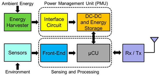
Figure 1.
General block diagram of an Internet-of-things end-node.
Figure 2 shows the general architecture of a PMU for EH purposes [14]. The start-up circuit allows the unit to cold-start from zero stored charge, when a minimum level of input power is available. This block can be implemented as a passive circuit [10] or with a low-power secondary converter like a Dickson charge pump [5]. During the start-up process, the undervoltage lockout (UVLO) block monitors the voltage level at the storage element (VST), and when the minimum operating value is reached, it sends a control signal to the main converter to start its operation. The main converter in the PMU can have either a switched-capacitor (SC) [3] or switched-inductor [5] implementation. It has been proved that inductor-based converters can harvest power from very low input voltages [15]. However, in order to show acceptable efficiency at the typical power levels of energy harvesting; they require to be implemented with a large external discrete component [6]. This increases the final cost and size of the PMU. On the other hand, SC topologies can be fully integrated [3] and still show similar performance for the same levels of input/output power.
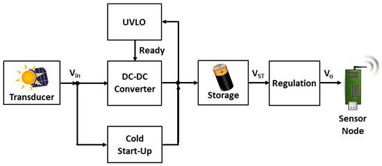
Figure 2.
Simple architecture of a power management unit for energy harvesting [14].
Table 1 lists a sample of commercial devices that represent the main blocks on the diagram of Figure 1. The typical quiescent (IQ) and active (IACT) current consumptions are also shown, and their sum is representative of the energy requirements of an IoT end-node. From Table 1, it is observed that the minimum instantaneous power consumption of a typical IoT node in standby mode is within the range of 10’s of microwatts. When actively sensing and transmitting data, the consumption of the node can then reach up to several 100’s of milliwatts. As a way to reduce the average power (PAVRG) consumed by the IoT system, it is commonly placed under a duty-cycled operation, as depicted in Figure 3.

Table 1.
Quiescent and active current consumption of sample off-the-shelf components for IoT.
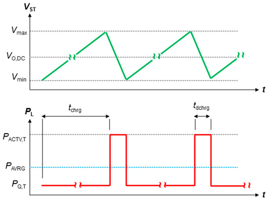
Figure 3.
Transient waveforms of the voltage at the storage element (VST) in the power management unit (PMU), and the power consumption of an IoT end-node in duty-cycled operation.
In Table 2, the specifications of various commercial transducers for EH are given, showing the available instantaneous output power that can be generated by those devices under specific conditions. It can be observed that the instantaneous power delivered by medium-size harvesters is below 100 mW, significantly less than what can be consumed by a typical IoT node during active operation. That is why the operation of the IoT node should be carefully designed such that there is a balance on the energy required in the active mode, and the energy that is being supplied by the harvesting devices over the standby period. If designed properly, the storage element at the output of the PMU (see Figure 2) will not get completely depleted, and its voltage (VST) can be maintained within the minimum and maximum values required by the final regulation stage of the PMU.

Table 2.
Output power characteristics of typical energy harvesting transducers.
Taking Figure 3 as a reference, the minimum value of the storage capacitor (CST) needed to constrain the drop in the output voltage (when the system is in active mode) can be calculated using:
where Idchrg is the total current consumed by the node in active operation, and tdchrg is the duration of this mode. Both Idchrg and tdchrh are defined by individual specs of the system’s components. Observe that a constant discharging current is considered in Equation (1), and that this is just an approximation of actual behavior.
Once the minimum value of storage capacitance is known, the minimum required standby time (in minutes) to allow CST to be charged back again to its maximum voltage can be calculated as:
A simple example illustrates the previous design procedure. Let’s assume a PMU delivers an output voltage of Vo = 3.3 V to an IoT sensor node system. This is a valid supply voltage for all the components listed in Table 1. If the PMU has an LDO in the regulation block, there is a minimum voltage that is needed at the storage capacitance. This voltage can be estimated as:
where VDO is the dropout voltage in the linear regulator. Assuming the use of a LP5907 regulator (see Table 1), then VDO = 200 mV for an output current of 250 mA. That gives VST,min = 3.5 V. The maximum voltage allowed in the storage capacitor would be given by the maximum value that the LP5907 tolerates at its input, that is VST,max = 5.5 V.
To calculate the minimum storage capacitance required in this example, we must know the duration of the active period in the sensor node (tdchrg) and the total current that is being drawn during this time. From Table 1 we observe that the current drawn from the CC3120 Wi-Fi processor is the dominant value over all other components, so we assume Idchrg ≈ 230 mA. If the active time is 10 ms, then:
The system requires a minimum time in the standby mode, to allow the storage capacitor to be charged once again to its maximum value (see Figure 3). For this calculation, we will assume the energy harvesting system is delivering a constant charging current of 100 μA. This has experimentally been found to be the approximate value for the charging current delivered by a low power PMU with 1.75 mW of input power [16], and will be used in our example. According to Equation (2), that makes tchrg,min ≈ 24 s. This represents a heavily duty-cycled operation with D ≈ 0.04%. Also, observe that the total quiescent current consumption of the IoT node (IQ ≈ 7.5 μA per Table 1) was neglected in the previous calculation, as well as the leakage current in the storage capacitor (estimated below 1 µA [16]). If we consider these extra current consumptions, the total charging time would have to increase its value by almost 10%.
Note that the charging time calculation has considered a constant charging current approximation, and assumes that the necessary ambient conditions for the energy harvesters (see Table 2) are present during all the charging period. If there is any interruption on those conditions, the required charging time would have to be extended. This discussion highlights the importance of multisource energy harvesting for system reliability and performance. Finally, one important design aspect is that the total power consumption of the PMU circuitry should be negligible when compared to the power delivered to the load (particularly during standby mode). This imposes design constraints for a PMU to operate in the regime of a few microwatts or even nanowatts [17,18,19]. This in itself is also a very challenging design goal.
3. Overview of Multisource Energy Harvesting Techniques
In this section we provide a review of published works on multiple-input energy harvesting. The works are categorized according to common features and techniques, and presented in an order of increasing complexity of the topologies used.
3.1. Simple methods for Multisource Energy Harvesting
3.1.1. Complementary Use of Energy Sources
The simplest method for multisource energy harvesting would be to mainly collect energy from a primary source, and then use a secondary transducer to only power up auxiliary circuits in the PMU. For example, the authors in [11] designed a two-input harvesting system for structural health monitoring of aircrafts. As shown in Figure 4, a thermal generator was used as the main source of power for the sensor network circuitry, while a piezoelectric transducer was applied to charge a small capacitor (Cbias), which provided the supply voltage to some bias and reference circuits.
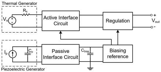
Figure 4.
Simplified architecture for complementary use of energy harvesting sources [11].
In the approach proposed in [11], the piezoelectric generator allowed for the early biasing of the active interface circuits at the airplane’s takeoff, when the power generated from the thermoelectric device is not enough to sustain the operation of the harvesting unit. Cold start-up of the system is then achieved through a passive interface and the complementary source of energy, eliminating the need of a battery. Note, however; that the described architecture does not really combine the energy coming from both input sources to deliver it to the load. Also, the reported circuit lacked a maximum power point tracking (MPPT) capability, which is a required feature to ensure maximum harvesting efficiency.
3.1.2. Power ORing
A simple and effective way of harvesting the energy coming from multiple sources is through a Power ORing architecture, as implemented in [12,20,21]. That is also the internal topology of the commercial devices LTC3331 from Linear Technology [22], and MB39C811 from Cypress Semiconductor [23]. As shown in Figure 5, this architecture offers a modular approach, capable of supporting an arbitrary number of harvesting subsystems connected in parallel through diodes. Another advantage of this approach is that each subsystem can independently perform MPPT on its own transducer [12,20], which helps increasing the tracking efficiency for each harvester source. The use of diodes in the Power ORing topology also ensures a self-synchronized operation, reducing the complexity of the PMU. If needed, a DC-DC converter can further process and regulate the output voltage according to the requirements of the load.
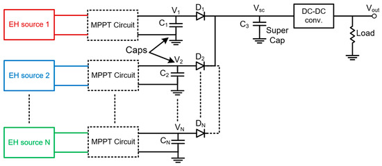
Figure 5.
Power ORing architecture for multiple input energy harvesting [12,20].
There are several disadvantages associated with the architecture shown on Figure 5. First, there are some extra power losses caused by the forward voltage drop on the diodes. Also, having an independent MPPT circuit for each harvester increases significantly the size and cost of the application, and comes with a significant overhead on its power consumption. This can be solved by eliminating the individual MPPT blocks, and controlling the DC-DC converter in such a way that the voltage at the storage capacitor (VSC) ensures the maximum transfer of power from the parallel connection of harvesters [21]. However, this comes at the expense of losing tracking efficiency for each individual transducer, especially for a large number of inputs [14]. Finally, it is important to observe that, in the system of Figure 5; the energy coming from all the harvesters is not really added-up. Rather, only the largest input voltage from V1, V2 … VN is selected and delivered to the output. This strategy works well for complementary harvesters (like solar and wind transducers), where usually it is not expected that they will be simultaneously delivering a significant amount of energy. However, the same scheme would offer a poor performance in scenarios where multiple heterogeneous harvesters are at the same time delivering different but comparable levels of energy.
3.1.3. Voltage Level Detection
With a more complex control scheme, the diodes in the circuit of Figure 5 can be replaced by voltage-controlled switches, reducing the power losses associated to these devices. The turning-on of the switches can be synchronized according to different strategies. For example, in [24] a voltage level detection strategy is implemented, and the charging of a microbattery is taken from either the voltage generated from a thermal or a RF harvesting subsystem, depending on which one exhibits a higher value. In [25], a better approach is taken: each input is sequentially connected to the output for a predefined period of time, provided their voltage is higher than a specific threshold. Finally, in [26], the operation of the control block also follows a voltage level-based criteria, this time associated with the state-of-charge of the storage battery. When the voltages at the output of the harvesting subsystems are less than a preset voltage Vmax, they are disconnected from the battery charging circuit till they charge up their corresponding output capacitors. The precise value of Vmax would depend on the battery type that is being used. The battery charger is disconnected when the output voltages of the subsystems decrease below a certain minimum threshold, and then connected back again when any of the capacitors reach Vmax.
The sequential nature of the algorithms proposed in [25,26] implies that there is no simultaneous harvesting of the energy coming from the multiple inputs, and that there is a potential waste of available power. Specifically, if a minimum value is being stablished for connecting an input to the storage element, then this connection may never occur even when such input is delivering a significant amount of power, but below of the predefined threshold. Given the unpredictable variation of ambient energy sources, the voltage level detection approach has limited applicability.
3.2. Architectures for Multiple Source Energy Combining
One thing that was generally noted for all the above topologies is that none of them effectively combines or adds the energy coming from each input. However, in the literature different schemes have been proposed to perform the combination of energy. These are going to be discussed next.
3.2.1. Energy Combining Through Linear Regulators
As shown in Figure 6, all the energy coming from three different sources (inductive link, piezoelectric and photovoltaic cells) is added in current form by connecting the output of individual linear regulators [27]. A single storage device (SSD external capacitor) is used to store the energy and stabilizing the LDOs. No battery charging mechanism is used in this scheme. The start-up mechanism (not shown in the Figure) occurs through a Power-on-Reset (POR) circuit: when the output voltage reaches a minimum value of 0.8-V, all the functional blocks are activated. The proposed architecture also allows to store the collected charges from each input in more than one output capacitor (MS1 to MS3). This multiple storage modes (determined by control bits C1, C2 and C3), provides up to three different output voltage rails with independent regulation.
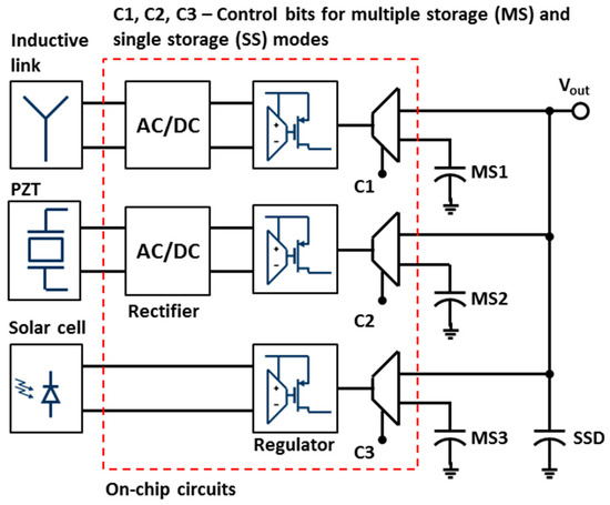
Figure 6.
Simplified scheme of a multiharvested circuit architecture using linear regulators [16].
As observed, the circuit of Figure 6 is capable of concurrently harvesting energy from multiple sources and requires of a simple control algorithm. However, the architecture requires of an LDO for each energy source, which compared with the switched-type of regulators, can be considered less efficient. Also, stabilization concerns limit the value of output capacitance that can be used, prohibiting the use of devices in the range of mF. Therefore, the number of practical uses for this kind of approach is rather limited.
3.2.2. Multiple-Input Boost Converter
Figure 7 shows a four input non-isolated boost converter that can be used for multisource energy harvesting. This converter can also be seen as a modified Dickson charge pump where each stage is fused with a boost converter [28]. In this topology, energy is extracted from every input source and used to charge the capacitor of the following stage. Simple duty-cycle control can be used for output voltage regulation according to the following equation:
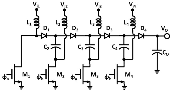
Figure 7.
Non-isolated multiple input boost converter proposed in [27].
The converter shown in Figure 7 has some important drawbacks. First of all, it requires of multiple inductors, making it a bulky and expensive solution. Also, Equation (5) shows an opposite effect of duty cycle on inputs 1 and 3 when compared with inputs 2 and 4, which means that a boosting ratio cannot be independently setup for each input source. Lastly, authors in [28] do not show if it is possible to implement any type of MPPT function on the converter.
3.2.3. Shared-Inductor DC-DC Converters
In the literature, buck-boost converters are commonly used in energy harvesting to create an impedance matching scheme for MPPT purposes, as the input impedance of the converter can be easily tuned via switching frequency control to create the required time-average input resistance. When multiple inputs are being considered, a single shared inductor scheme can be used on the buck-boost converter to reduce the number of external components that are needed [29]. Figure 8 depicts a simplified schematic of this type of architecture [18], where 5 interface channels are given to AC (piezoelectric) input types and 4 to DC (solar or thermal) input types. The complex controller in this topology must allow all the inputs to have access to the single inductor, while at the same time ensuring that maximum transfer of power is obtained for each one of them.
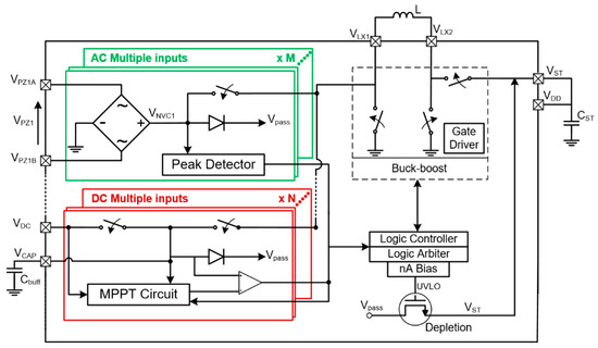
Figure 8.
Buck-boost based energy combiner with shared inductor scheme [18].
In [18], a fractional open circuit voltage (FOCV) method is used for MPPT of the DC inputs. Open circuit conditions (OCC) are created by disconnecting each harvester from the interface, and then waiting for the voltage to restore to its open circuit value. Small capacitors are then used to sample and hold the voltage. In order to reduce the time required for the input voltage to reach the OCC, the input buffer capacitor (Cbuff) is not directly connected to the harvester, but through an extra pin in the circuit (VCAP). Thus, 2 external pins per harvester are needed; as shown in Figure 8. This approach reduces the required sampling time down to 2-µs, and the operation is repeated every 8 energy-extraction cycles of the boost converter (i.e., every 25 ms). This scheme allows following the variations of the input voltage, and reducing the wasted energy in the FOCV sampling process when the harvester is disconnected.
To regulate the access to the converter, an arbiter logic circuit was implemented, with preset priorities fixed for each harvester type. Piezoelectric harvesters were set to the highest priorities as power can only be extracted when their output voltage reaches its maximum [18]. Other type of harvesters (solar and TEG) were set to a lower priority, as their output power pattern is almost constant with time.
In the circuit of Figure 8, MPPT also requires the use of a comparator to control the switching speed in the boost converter, maintaining the harvester voltage close to the ideal OCC for maximum power extraction. Fast comparators are then needed to maintain good MPPT tracking accuracy, and they come with higher power consumption. In [19] this problem is solved by using a shared comparator for all input sources, and then tuning an oscillator to mimic the output of the comparator. The oscillator (one for each source) continues the MPPT operation, and the comparator is powered down to save power. With this strategy, power can be harvested even at the nanowatts level [19].
In [30], a structure similar to the one in Figure 8 is also used for multiple input harvesting. However, the MPPT algorithm is rather implemented with a time-multiplexing approach, and not priority-based as in the case of [18]. Rather, a microcontroller is used to monitor the MPPT process; seeking to maximize the product, according to the following equation:
In Equation (6), Rem is the emulated resistance of the boost converter, TCLK is the switching period and L is the inductor’s value. Also, Ni is the number of clock cycles given to the ith-input and NT is the total number of clock cycles. The previous approach is similar to a hill-climbing algorithm [3], but with a simplified sensing scheme that does not require the measurement of current, as it is replaced by Ni as a parameter that reflects the average current extracted from the harvester.
The main disadvantage of the shared-inductor architecture is that, as the numbers of input sources are increased; the operation deviates from a truly concurrent energy harvesting, as all but one transducer is left disconnected. This effect can be reduced with a larger input buffer capacitor, as they store the energy while the harvester is disconnected but, as mentioned before, it impacts the OC voltage settling time for the MPPT method. This in turn establishes a tradeoff between tracking accuracy and harvesting efficiency.
3.2.4. Fully Integrated Switched-Capacitor Converter for Concurrent Energy Harvesting
It is well known that switched-capacitor (SC) circuits can be used to add voltages. The basic concept of a SC-based DC combiner is shown in Figure 9 [31]. The technique consists of converting a DC input into an AC form, then superimposing it on another DC input. By rectifying the resulting waveform, a DC output voltage can then be obtained. As shown in Figure 9, this process can be cascaded in a modular fashion to combine an arbitrary number of inputs.

Figure 9.
Basic concept of a switched capacitor based (i.e., fully integrated) DC power combiner for energy harvesting.
One implementation of the switched-capacitor unit for the DC combiner is shown in Figure 10 [31]. This circuit is capable of combining two DC sources. In this topology, input In2 is converted into AC form using a differential low-power oscillator (I0) composed of thyristor-based delay cells. Then, with the help of drivers I1 and I2, the pulsed-shaped waveform is coupled to the intermediate nodes (vA and vB) through capacitors C1 and C2. The peak-to-peak voltage of nodes vA and vB would equal to Vi1 + Vi2 which is further rectified by the transistor pair M3-M4. If a large capacitor is connected at the output node of the circuit, Vout will consist of a DC voltage equivalent to the sum of both inputs.
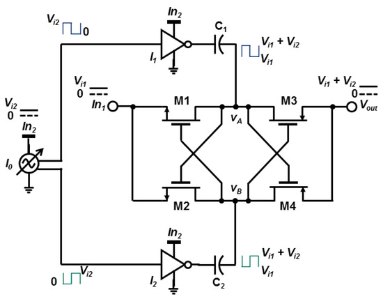
Figure 10.
Two-input DC switched-capacitor combiner, which is used as a module for the architecture shown in Figure 9.
In [31], it is shown that an accumulation process of the voltages occurs at the output node of the circuit in Figure 10. This addition of the input voltages occurs through an accumulation of electric charges in the coupling capacitors C1 and C2. The capacitors are first charged to the voltage Vi1 implying the storage of a certain amount of energy. When the voltage at those capacitors is increased to Vi1 + Vi2, the extra charge that has been stored represents an increase in the available energy on the capacitors, resulting in the addition of energies coming from the two individual sources.
The SC-based energy combiner of Figure 10 has several advantages over their inductor-based counterparts described in the previous subsection. First, it can be fully integrated, reducing the size and cost of the implementation. Also, the energy harvesting from multiple sources occurs in a concurrent way. There is not a multiplexing of inputs, imposed by the necessity of sharing a common resource as the single-inductor topology. As mentioned before, this multiplexing involves a trade-off between tracking accuracy and harvesting efficiency that is intensified by a larger number of inputs.
3.2.5. Performance Comparison of Multisource Energy Harvesting Architectures
In many cases it is difficult to compare the performance of different works found in the literature, especially when diverse technologies were used for each implementation. Most of the works also use different transducer models, so the value of total output power that is measured and reported will logically differ. However, in Table 3 a comparison is made on the performance of the various multisource energy harvesting topologies that were reviewed in this paper. We have rather focused on topological traits and capabilities, like being able to perform MPPT and battery charging operations. Peak efficiency can also be compared because it is a normalized quantity that is related to the architecture’s complexity and serves as a standard figure of merit for PMUs. The input power (when available) at which the peak efficiency is measured is included as a reference. Another important figure-of-merit is the quiescent current consumption of each implementation, and it is also included on the comparison table.

Table 3.
Comparison of multisource energy harvesting architectures.
4. Conclusions and Open Areas of Research
The Internet-of-Things “revolution” has been the driving force for many research efforts in different areas of electronic circuits and computer systems. Energy harvesting techniques has been extensively investigated as they promise to be a key enabling technology for autonomous IoT end-nodes. In particular, multisource energy harvesting has demonstrated to be a better option for system reliability.
Different architectures have been proposed for harvesting energy from multiple inputs, each of them suitable for a particular application. The simpler schemes such as the complementary use of harvesters or Power ORing topologies offer reduced system complexity and modularity, making them acceptable solutions when it is not expected that all the input sources will be delivering a significant amount of power at the same time. Energy combining has been demonstrated with multiple input switched-inductor or switched-capacitor converter architectures. As observed, the time-multiplexing nature of the shared-inductor scheme imposes a tradeoff between tracking accuracy and efficiency. In contrast, the SC approach described in this paper offers concurrent energy addition with a fully integrated approach, but its functionality and performance can still be improved. The reported architecture in [31] lacks an automatic MPPT control and battery charging functionality. The design of a complete integrated solution based on the SC unit block of Figure 10 (or other similar) is still to be investigated. A potential limitation inherent to the energy combiner scheme of Figure 9 would be the limited number of inputs that the system can accommodate, given a maximum Silicon area allocated to the converter. To increase the total number of inputs without increasing the area consumed by the integrated capacitors, some type of sharing scheme would have to be proposed. Also, algorithms could also be implemented for smart energy harvesting, where input sources can be selected depending on their available power. Intelligent battery-charging functionality, according to the levels of harvested power, is also an open area of research that has not been well explored. To date, none of these features have been found in state-of-the-art multisource harvesting architectures.
Acknowledgments
This work was supported in part by Intel, Texas Instruments, Qualcomm, CONACYT and UADY.
Author Contributions
Johan J. Estrada-López is the main author and thus responsible for writing the paper. Amr Abuellil has contributed with Section 3.2.3 about shared-inductor converters and creation of figures, Zizhen Zeng has contributed with Section 3.2.1 and Edgar Sánchez-Sinencio has been responsible for revising and supervising the paper.
Conflicts of Interest
The authors declare no conflict of interest.
References
- Al-Fuqaha, A.; Guizani, M.; Mohammadi, M.; Aledhari, M.; Ayyash, M. Internet of Things: A Survey on Enabling Technologies, Protocols, and Applications. IEEE Commun. Surv. Tutor. 2011, 17, 2347–2376. [Google Scholar] [CrossRef]
- Stankovic, J.A. Research Directions for the Internet of Things. IEEE IoT J. 2014, 1, 3–9. [Google Scholar] [CrossRef]
- Liu, X.; Huang, L.; Ravichandran, K.; Sánchez-Sinencio, E. A Highly Efficient Reconfigurable Charge Pump Energy Harvester with Wide Harvesting Lange and Two-Dimensional MPPT for Internet of Things. IEEE J. Solid-State Circuits 2016, 51, 1302–1312. [Google Scholar] [CrossRef]
- Khosro Pour, N.; Krummenacher, F.; Kayal, M. Fully Integrated Solar Energy Harvester and Sensor Interface Circuits for Energy-Efficient Wireless Sensing Applications. J. Low Power Electron. Appl. 2013, 3, 9–26. [Google Scholar] [CrossRef]
- Rozgic, D.; Markovic, D. A Miniaturized 0.78-mW/cm2 Autonomous Thermoelectric Energy-Harvesting Platform for Biomedical Sensors. IEEE Trans. Biomed. Circuit Syst. 2017, 11, 773–783. [Google Scholar] [CrossRef] [PubMed]
- Ramadass, Y.K.; Chandrakasan, A.P. An Efficient Piezoelectric Energy Harvesting Interface Circuit Using a Bias-Flip Rectifier and Shared Inductor. IEEE J. Solid-State Circuits 2010, 45, 189–204. [Google Scholar] [CrossRef]
- Zhao, J.; Ramadass, Y.; Lang, J.; Ma, J.; Buss, D. Bias-Flip Technique for Frequency Tuning of Piezo-Electric Energy Harvesting Devices. J. Low Power Electron. Appl. 2013, 3, 194–214. [Google Scholar] [CrossRef]
- Oh, T.; Islam, S.K.; Mahfouz, M.; To, G. A Low-Power CMOS Piezoelectric Transducer Based Energy Harvesting Circuit for Wearable Sensors for Medical Applications. J. Low Power Electron. Appl. 2017, 7, 33. [Google Scholar] [CrossRef]
- Bertacchini, A.; Larcher, L.; Maini, M.; Vincetti, L.; Scorcioni, S. Reconfigurable RF Energy Harvester with Customized Differential PCB Antenna. J. Low Power Electron. Appl. 2015, 5, 257–273. [Google Scholar] [CrossRef]
- Yang, G.; Stark, B.H.; Hollis, S.J.; Burrow, S.G. Challenges for Energy Harvesting Systems Under Intermittent Excitation. IEEE J. Emerg. Sel. Top. Circuits Syst. 2014, 4, 364–374. [Google Scholar] [CrossRef]
- Vankecke, C.; Assouère, L.; Wang, A.; Durand-Estèbe, P.; Caignet, F.; Dilhac, M.-J.; Bafleur, M. Multisource and Battery-Free Energy Harvesting Architecture for Aeronautics Applications. IEEE Trans. Power Electron. 2015, 30, 3215–3227. [Google Scholar] [CrossRef]
- Carli, D.; Brunelli, D.; Benini, L.; Ruggeri, M. An effective multi-source energy harvester for low power applications. In Proceedings of the Design, Automation & Test in Europe, Grenoble, France, 14–18 March 2011. [Google Scholar] [CrossRef]
- Lundager, K.; Zeinali, B.; Tohidi, M.; Madsen, J.K.; Moradi, F. Low Power Design for Future Wearable and Implantable Devices. J. Low Power Electron. Appl. 2016, 6, 20. [Google Scholar] [CrossRef]
- Romani, A.; Tartagni, M.; Sangiorgi, E. Doing a Lot with a Little: Micropower Conversion and Management for Ambient-Powered Electronics. Computer 2017, 50, 41–49. [Google Scholar] [CrossRef]
- Carlson, E.J.; Strunz, K.; Otis, B.P. A 20 mV Input Boost Converter with Efficient Digital Control for Thermoelectric Energy Harvesting. IEEE J. Solid-State Circuits 2010, 45, 741–750. [Google Scholar] [CrossRef]
- Carreon-Bautista, S.; Huang, L.; Sanchez-Sinencio, E. An Autonomous Energy Harvesting Power Management Unit With Digital Regulation for IoT Applications. IEEE J. Solid-State Circuits 2016, 51, 1457–1474. [Google Scholar] [CrossRef]
- Chowdary, G.; Chatterjee, S. A 300-nW Sensitive, 50-nA DC-DC Converter for Energy Harvesting Applications. IEEE Trans. Circuits Syst. 2015, 62, 2674–2684. [Google Scholar] [CrossRef]
- Dini, M.; Romani, A.; Filippi, M.; Bottarel, V.; Ricotti, G.; Tartagni, M. A Nanocurrent Power Management IC for Multiple Heterogeneous Energy Harvesting Sources. IEEE Trans. Power Electron. 2015, 30, 5665–5680. [Google Scholar] [CrossRef]
- Chowdary, G.; Singh, A.; Chatterjee, S. An 18 nA, 87% Efficient Solar, Vibration and RF Energy-Harvesting Power Management System With a Single Shared Inductor. IEEE J. Solid-State Circuits 2016, 51, 2501–2513. [Google Scholar] [CrossRef]
- Li, H.; Zhang, G.; Ma, R.; You, Z. Design and Experimental Evaluation on an Advanced Multisource Energy Harvesting System for Wireless Sensor Nodes. Sci. World J. 2014. [Google Scholar] [CrossRef] [PubMed]
- Tan, Y.K.; Panda, S.K. Energy Harvesting From Hybrid Indoor Ambient Light and Thermal Energy Sources for Enhanced Performance of Wireless Sensor Nodes. IEEE Trans. Ind. Electron. 2011, 58, 4424–4435. [Google Scholar] [CrossRef]
- Linear Technology. Nanopower Buck-Boost DC/DC with Energy Harvesting Battery Charger. Available online: http://cds.linear.com/docs/en/datasheet/3331fc.pdf (accessed on 1 March 2018).
- Cypress Semiconductor. Ultra Low Power Buck Power management IC for Solar and Vibrations Energy Harvesting. Available online: http://www.cypress.com/file/246676/download (accessed on 1 March 2018).
- Lhermet, H.; Condemine, C.; Plissonnier, M.; Salot, R.; Audebert, P.; Rosset, M. Efficient Power Management Circuit: Thermal Energy Harvesting to Above-IC Microbattery Energy Storage. In Proceedings of the IEEE International Digest of Technical Papers Solid-State Circuits Conference, San Francisco, CA, USA, 11–15 February 2007; pp. 62–587. [Google Scholar] [CrossRef]
- Kang, T.; Kim, S.; Hyoung, C.; Kang, S.; Park, K. An Energy Combiner for a Multi-Input Energy-Harvesting System. IEEE Trans. Circuits Syst. II Express Briefs 2015, 62, 911–915. [Google Scholar] [CrossRef]
- Amanor-Boadu, J.; Abouzied, M.A.; Carreon-Bautista, S.; Ribeiro, R.; Liu, X.; Sanchez-Sinencio, E. A switched mode Li-ion battery charger with multiple energy harvesting systems simultaneously used as input sources. In Proceedings of the 2014 IEEE 57th International Midwest Symposium on Circuits and Systems (MWSCAS), College Station, TX, USA, 3–6 August 2014; pp. 330–333. [Google Scholar] [CrossRef]
- Colomer-Farrarons, J.; Miribel-Catala, P.; Saiz-Vela, A.; Samitier, J. A Multiharvested Self-Powered System in a Low-Voltage Low-Power Technology. IEEE Trans. Ind. Electron. 2011, 58, 4250–4263. [Google Scholar] [CrossRef]
- Colalongo, L.; Dotti, D.; Richelli, A.; Kovács-Vajna, Z.M. Non-isolated multiple-input boost converter for energy harvesting. Electron. Lett. 2017, 53, 1132–1134. [Google Scholar] [CrossRef]
- Bandyopadhyay, S.; Chandrakasan, A.P. Platform Architecture for Solar, Thermal, and Vibration Energy Combining With MPPT and Single Inductor. IEEE J. Solid-State Circuits 2012, 47, 2199–2215. [Google Scholar] [CrossRef]
- Shi, C.; Miller, B.; Mayaram, K.; Fiez, T. A Multiple-Input Boost Converter for Low-Power Energy Harvesting. IEEE Trans. Circuits Syst. II Express Briefs 2011, 58, 827–831. [Google Scholar] [CrossRef]
- Abouzied, M.; Osman, H.; Vaidya, V.; Ravichandran, K.; Sanchez-Sinencio, E. An Integrated Concurrent Multiple-Input Self-Startup Energy Harvesting Capacitive-Based DC Adder Combiner. IEEE Trans. Ind. Electron. 2017. [Google Scholar] [CrossRef]
© 2018 by the authors. Licensee MDPI, Basel, Switzerland. This article is an open access article distributed under the terms and conditions of the Creative Commons Attribution (CC BY) license (http://creativecommons.org/licenses/by/4.0/).