1. Introduction
Energy harvesting has become an attractive way to power wirelessly connected electronic systems such as sensors without using batteries or other energy source with limited lifetime. The research in this field has been very intense in the last years, and solutions harvesting energy from a large set of sources such as solar light, thermal gradient, strain, vibrations, electromagnetic field, air flow, pressure variations, have been proposed.
Among the various options, the idea of exploiting the background RF signals as a power source for wireless devices is very attractive, especially due to the pervasive diffusion of RF signals used in modern communication systems. Unfortunately, the power associated with communication signals is unpredictable and typically very small, thus making it very difficult to use for providing the power supply also of very low-power devices such as sensors. To overcome this limit, the electromagnetic field for remote powering applications can be generated ad hoc.
The remote powering exploiting RF signals (e.g., Industrial Scientific and Medical (ISM) band [
1,
2]) is very attractive from the application point of view, as the radiated electromagnetic field can reach locations (in the environment, on industrial machineries, in industrial plants), where no other kind of power sources is available and cables are difficult to be placed. In this respect, the remote wireless powering is exploited, for example, in bionic systems [
3] and to power ultra-low-power devices like wireless sensor nodes [
4,
5]. The remote powering system is generally comprised of an antenna, an RF-DC power converter, and a power management circuit. The rectification circuits used to convert the RF power into a DC voltage is the most challenging building block of the whole system, whose optimization in terms of both conversion efficiency and sensitivity requires one to devise innovative solutions reducing the minimum power threshold needed for circuit operations.
Typically, in order to maximize the RF power gathered by the antenna, resonant matching networks are used to couple efficiently the Integrated Circuit (IC) converter with the antenna. Unfortunately, matching networks limit the frequency of operations around the resonance frequency, which is a problem in the case the signal/carrier frequency is not known a priori. Extending the frequency band of operations is thus highly desirable, as well as devising circuit solutions compensating the frequency shifts due to the unpredictable parasitic effects arising from the connection of the antenna to the converter IC. In this respect, the broadband co-design of the antenna and the IC converter is a key step to improve the efficiency and sensitivity performances of the whole system.
In this scenario, we present the design of an RF-DC energy conversion system comprised of the antenna and the IC converter. A reconfigurable differential RF-DC power converter architecture is selected to improve both conversion efficiency and sensitivity [
6]. The converter is combined with a matched broadband PCB antenna [
7] to enable the use of the RF energy conversion system at different frequencies in the ISM band. In order to minimize the power losses, no matching networks are used, and the antenna is designed to have an impedance matching the highly capacitive input of the IC converter.
Several papers presented in the literature focus on just one component (i.e., antenna or RF-DC converter) of an RF energy harvester. Differently from these contributions, this paper is focused on the presentation of a possible solution of a complete RF-DC energy harvesting system.
In particular, the issues related to the efficient combining of different system blocks are presented. Moreover, the whole system has been completely characterized by measurements carried out on the realized prototypes. The obtained results concerns the performance of the whole system, which is one of the most important things from an application point of view. Usually, the system architecture has to be chosen as a trade-off between opposite requirements of the single functional blocks, and combining the best solutions of each stand-alone component could not lead to the best performances of the whole system. For these reasons, we focused on the characterization of the whole system, in order to present some considerations and guidelines which can be used in the design of completely new RF energy harvesting systems.
The paper is organized as follows: The whole system is described in
Section 2. The characterization results of the integrated circuit implementing the RF-DC converter and the smart voltage regulator are described in
Section 3. In
Section 4, we described the performances of the whole system. Conclusions are given in
Section 5.
2. System Description
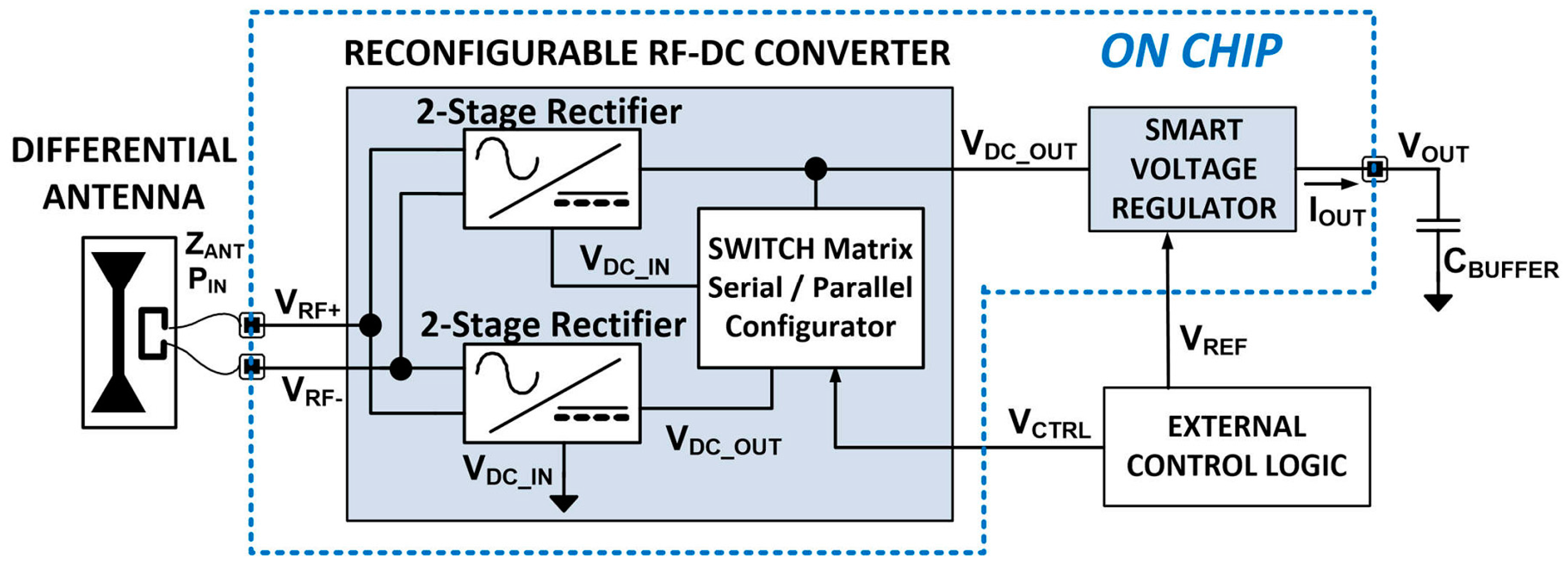
Figure 1 shows the RF energy harvesting system that we developed. It is comprised of (i) a custom differential antenna that gathers the incident RF energy; (ii) an RF-DC converter exploiting a reconfigurable architecture, which converts the RF power into a quasi-constant voltage supply; (iii) an output voltage regulator providing a constant DC voltage supply to an electrical load (e.g., an ULP wireless sensor node); (iv) an external logic circuit controlling the reconfigurable RF-DC converter.
Compared to classical solutions [
6] the use of a reconfigurable architecture for the RF-DC converter allows for improving both efficiency and sensitivity of the whole system. At the same time, the use of a differential antenna designed to match the input impedance of the rectifier simplifies the overall system design, while improving the overall efficiency, as the power losses associated with the parasitics of the matching network that would be needed are intrinsically avoided.
2.1. Reconfigurable Differential RF-DC Converter
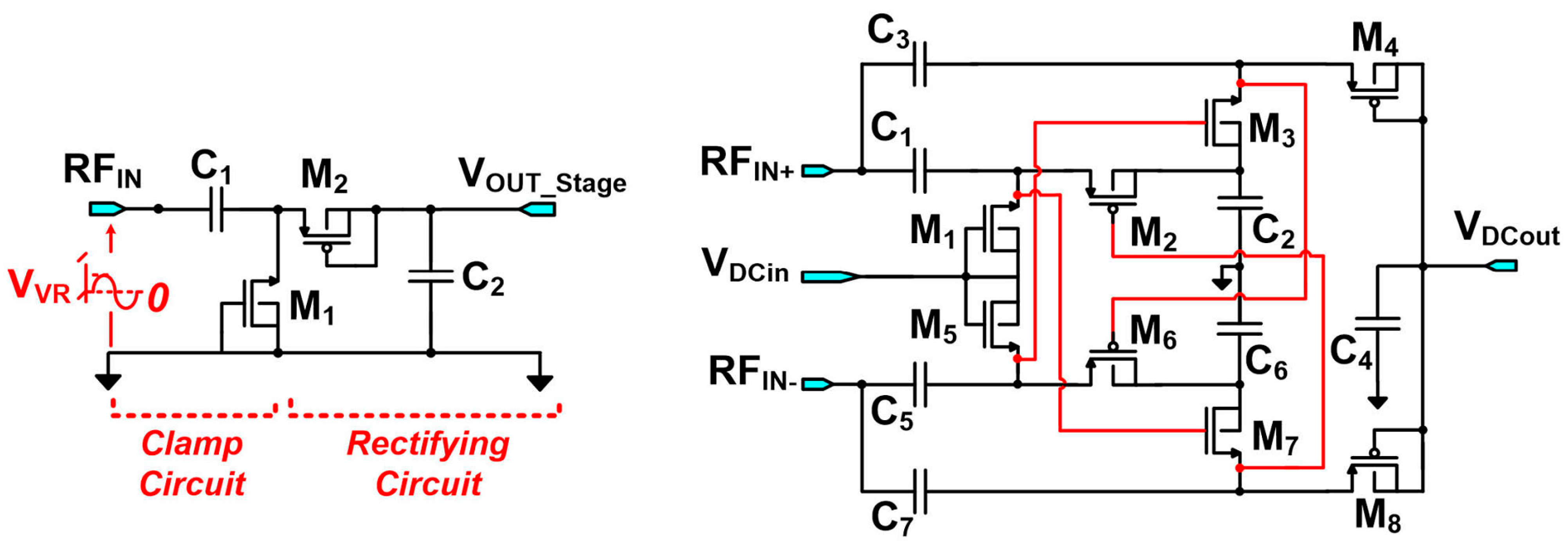
The reconfigurable RF-DC converter represents the core of the whole RF-DC energy harvesting system. It is comprised of two differential rectifier blocks derived from the classical two-stage Dickson voltage rectifier/multiplier [
8] shown in
Figure 2.
Each stage of the rectifiers is comprised of a clamp and rectifying sections: the clamp section adds a DC offset to the sinusoidal input voltage
VVR, while the rectifying section clamps the voltage to its maximum value. The steady state output voltage
VOUT_Stage depends on the input voltage amplitude,
VVR, and the voltage drop,
VM, across the transistors in diode configurations. Under the reasonable assumptions of identical transistors and negligible voltage drop across the large input capacitance,
VOUT_Stage can be calculated as
It is evident that maximizing the efficiency of the voltage rectifier requires to minimize
VM, which requires adopting Metal-Oxide-Semiconductor Field-Effect Transistors (MOSFETs) with minimum threshold voltage, reverse current and on-resistance. This technology requirement is alleviated by the differential rectifier topology, which, thanks to the cross-connection scheme shown in
Figure 2, allows for doubling the gate-source voltage of the MOSFETs compared to the classic diode-connected solutions. This is beneficial for the system efficiency, because it reduces the detrimental effects due to the threshold voltage of the MOSFETs. A detailed description of the operations of this proposed connection scheme is provided in [
6].
Figure 1.
RF energy harvester system comprised of the custom differential antenna, the RF-DC converter, the voltage regulator, the external control logic controlling the converter reconfiguration, and the external capacitor CBUFFER used for energy storage.
Figure 1.
RF energy harvester system comprised of the custom differential antenna, the RF-DC converter, the voltage regulator, the external control logic controlling the converter reconfiguration, and the external capacitor CBUFFER used for energy storage.
Figure 2.
Basic cell of a classic Dickson voltage rectifier/multiplier (left) and the proposed two-stage reconfigurable differential rectifier block with cross connection scheme highlighted (right).
Figure 2.
Basic cell of a classic Dickson voltage rectifier/multiplier (left) and the proposed two-stage reconfigurable differential rectifier block with cross connection scheme highlighted (right).
As shown in
Figure 1, the two rectifier blocks can be connected either in series or in parallel by means of a CMOS Switch Matrix controlled by the External Control Logic accordingly to the available input RF power. Changing the connection between the two rectifier blocks allows modifying the number of stages of the whole RF-DC converter: a two-stage (four-stage) converter corresponds to the case of a parallel (series) connection. In turn, this allows for modifying the resistive part of the input impedance of the converter,
ZD, modeled by the parallel of
RD and
CD, as shown in
Figure 3, where
CD accounts for the MOSFETs parasitic capacitance, while
RD depends on the load and the active power flowing into the rectification circuit. Since
RD depends also on the RF input power
PIN [
6], changing the rectifier connection allows for modifying
RD to match the resistance of the antenna impedance
ZANT =
RANT +
jXANT at different
PIN level. This allows for reducing the mismatch power losses due to the power-dependent variation of the input RF-DC converter, thus improving the efficiency of the matching network over a wider
PIN range. The impedance matching between the antenna and the converter is designed to account for the parasitic capacitance of the pad
CPAD, and the ohmic power losses due to the bonding parasitic resistance,
RBond, and inductance
LBond, which are included into the input impedance model, as shown in
Figure 3, [
9]. Furthermore, the reconfigurable circuit solution devised for the RF-DC converter allows for minimizing the efficiency reduction due to the
RD variation caused by the voltage regulator operation.
Figure 3.
Equivalent circuit used for the design of the impedance matching between the antenna and the differential RF-DC converter. ZANT is the antenna impedance; LBond and RBond are the parasitic resistance and inductance of the two bondwires, respectively; CPAD is the pad capacitance; ZD is the input impedance of the differential RF-DC converter within the ISM band modeled as the parallel of the the equivalent resistance RD and the equivalent capacitance CD.
2.2. Smart Output Voltage Regulator
The Smart Voltage Regulator (SVR) has been designed to keep the converter output voltage,
VOUT, at the constant reference voltage
VREF = 2 V. With reference to
Figure 1,
VREF is set by the external control logic.
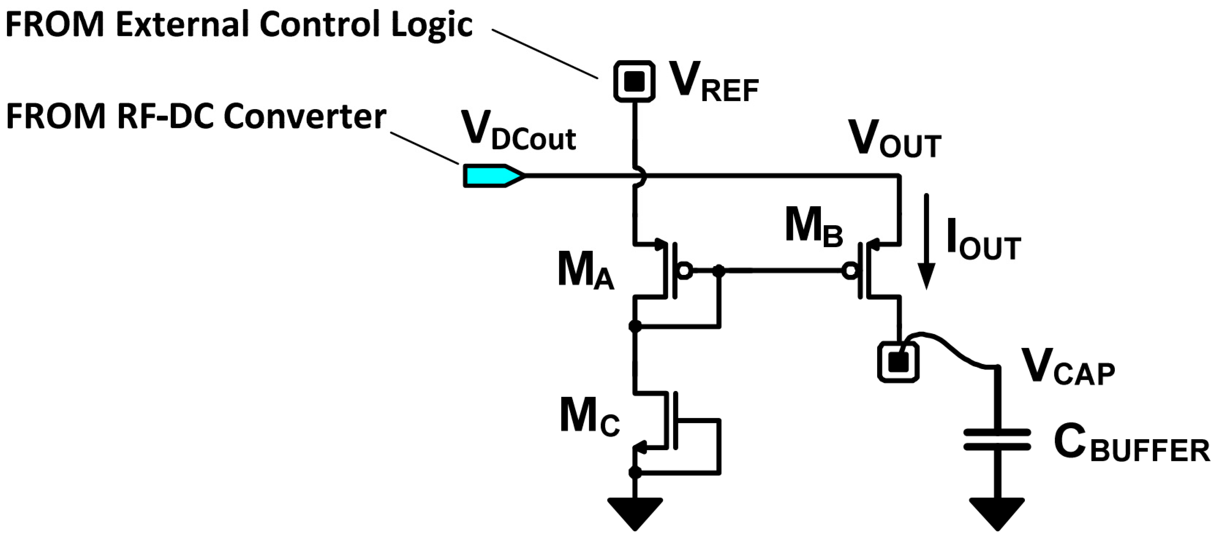
The operating principle of the SVR circuit, which resembles a classical current mirror, is very simple. With reference to
Figure 4, the transistors
MA and
MC keep constant the gate voltage of the transistor
MB. When the available antenna input power
PIN increases (decreases),
VOUT is forced to rise (fall). The higher (lower)
VOUT determines an increase (decrease) of the source-gate voltage of
MB, hence also the current drained by
MB increases (decreases). The lower (higher) equivalent DC resistance at the output of the RF-DC Converter forces the decrease (increase) of
VOUT, counteracting the initial
VOUT variation. Therefore, the SVR behaves as an active load.
Besides keeping the output voltage constant, the SVR significantly benefits the overall circuit efficiency compared to solutions employing either voltage limiters or LDO regulators. In fact, with the proposed solution, the output current, IOUT, charging the external buffer capacitor, CBUFFER, is modulated according to the available input power PIN. This allows for storing the excess input power into CBUFFER, while keeping constant the power dissipated across MB. Thus, the SVR efficiency remains constant regardless the operating conditions.
Figure 4.
Transistor level implementation of the Smart Voltage Regulator.
Figure 4.
Transistor level implementation of the Smart Voltage Regulator.
2.3. Custom Differential Antenna
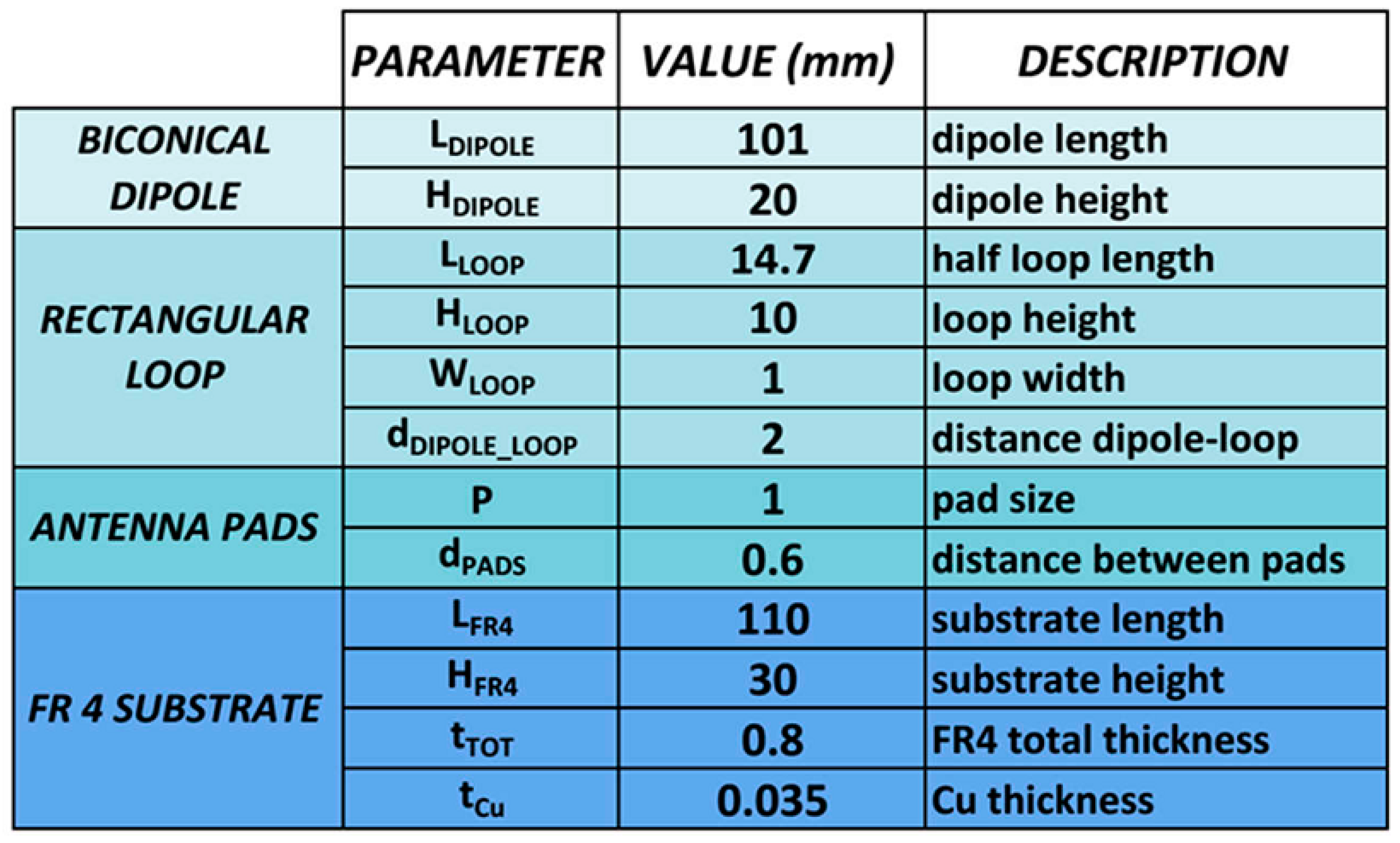
The custom differential antenna has been realized on a low cost FR4 substrate and exploits a layout reproducing a printed bi-conical radiating dipole with linear polarization. A rectangular loop couples inductively the dipole with the chip, as shown in
Figure 5. This topology has been chosen because it allows one to adjust independently the real and the imaginary parts of the antenna impedance acting on the size of the loop and its distance from radiating dipole [
10].
Figure 5.
Layout of the differential antenna realized on a FR4 substrate (up) and geometrical parameters of the antenna (down).
Figure 5.
Layout of the differential antenna realized on a FR4 substrate (up) and geometrical parameters of the antenna (down).
This significantly simplifies the design procedure, which requires one to match the antenna resistance and reactance to the converter impedance in order to maximize the power transfer and conversion. To this purpose, we also included the pad parasitic capacitance CPAD = 200 fF, and the impedance of the bond-wires used to connect the antenna to the IC, which have a resistance and an inductance of RBond = 2 Ω and LBond = 1 nH, respectively.
For the antenna design, we used the electromagnetic simulations performed with the CST Microwave Studio Software, which allowed including the effect of the antenna substrate, i.e., FR4 with relative dielectric permittivity εr = 4.3 and thickness of 0.8 mm. The antenna was designed by assuming an input impedance of the voltage regulator with RD = 10 kΩ and CD = 400 fF, with a pad and bonding parasitics equal to CPAD = 200 fF, RBond = 2 W, and LBond = 1 nH, respectively.
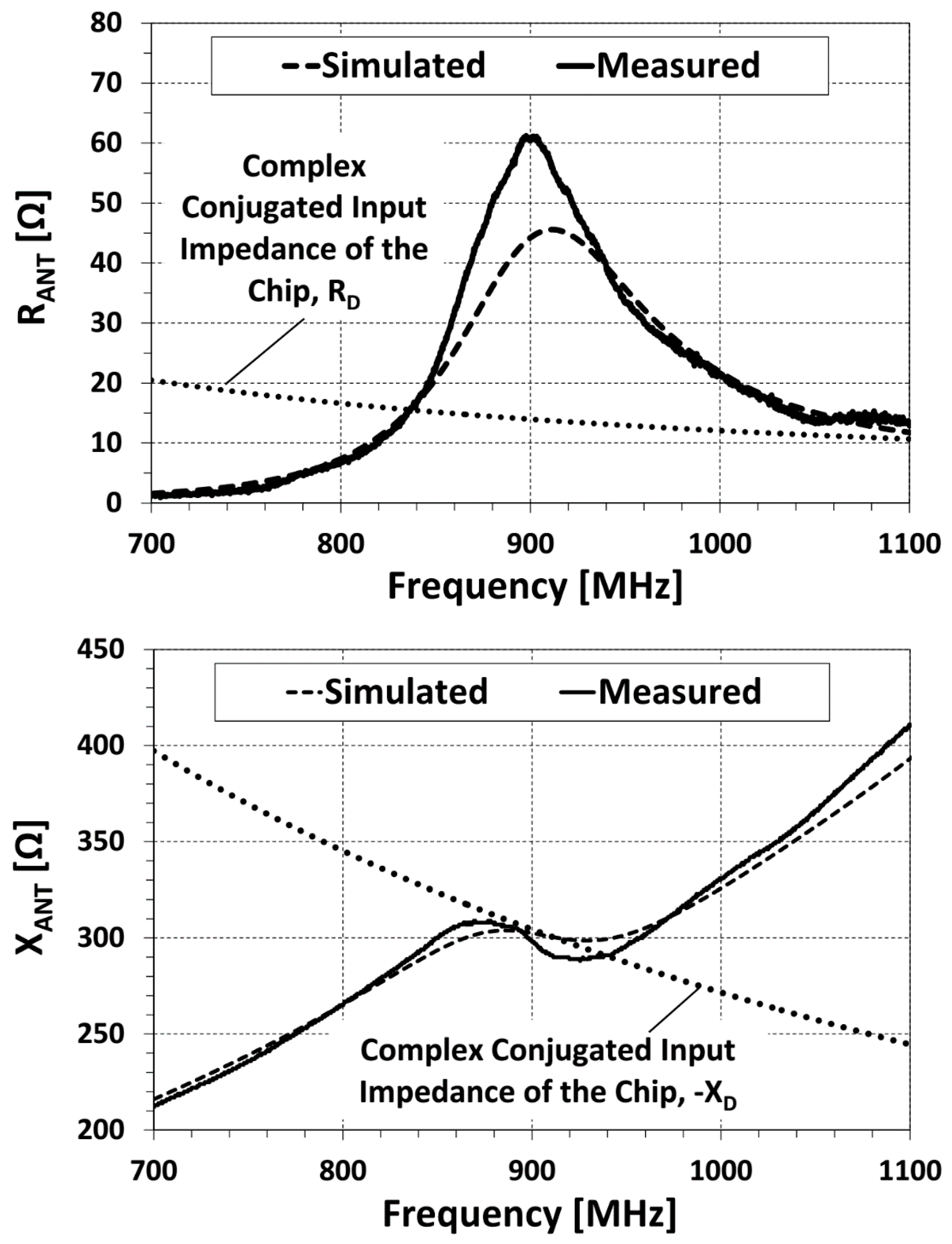
Unfortunately, the impedance matching can be effective only around the resonance frequencies, and, therefore, the design of a broadband antenna results in a very challenging task. In order to widen the band of the antenna, we designed the antenna so that its imaginary part matches the rectifier input capacitance at 900 MHz whereas the real one is at 840 MHz [
11]. In addition, the bi-conical shape of the radiating element allows further increasing the bandwidth. Simulation results, compared with the measured ones, are shown in
Figure 6.
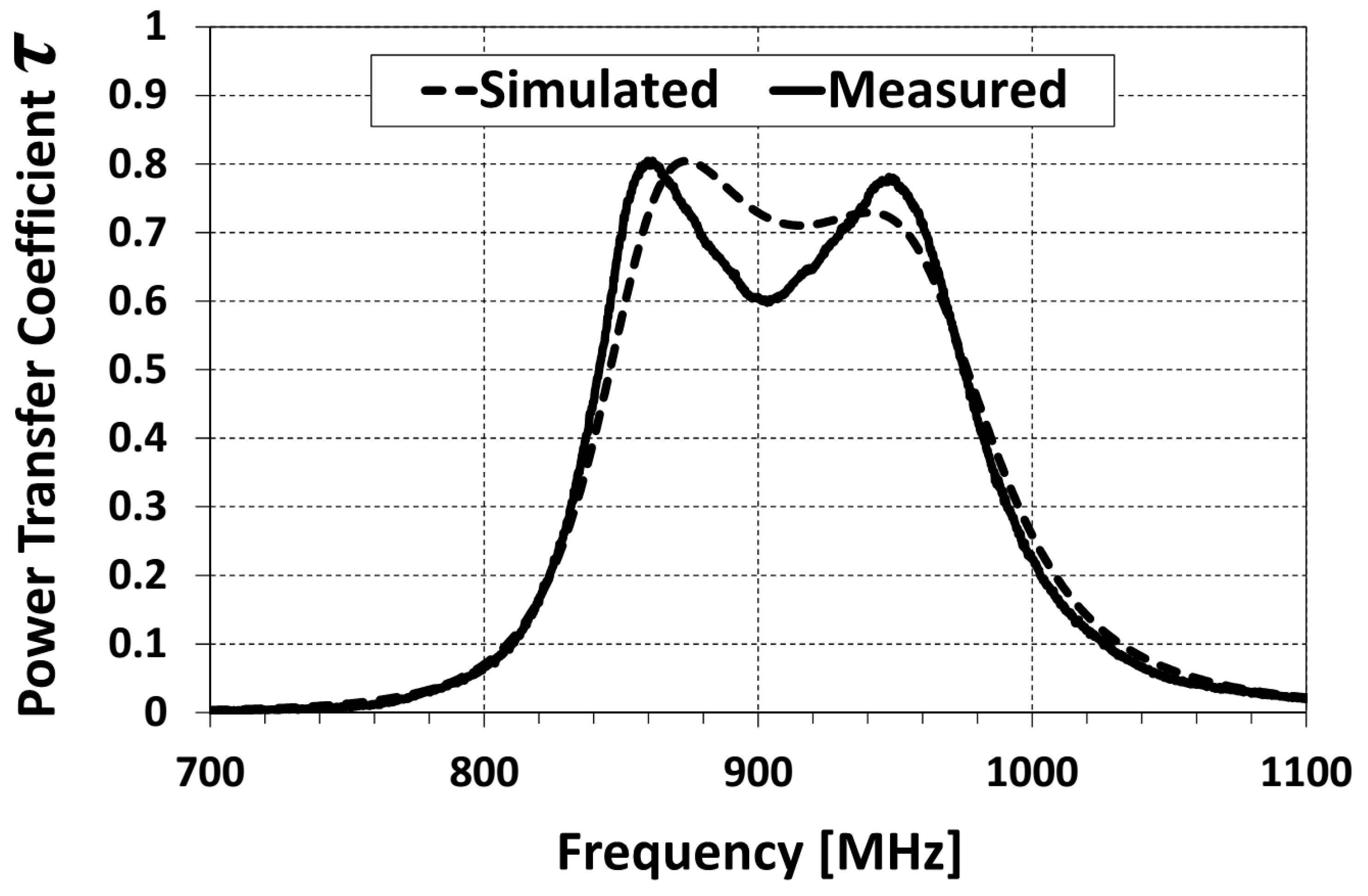
The slight penalty paid in terms of power transfer is widely compensated by the larger bandwidth as shown in
Figure 7 where the power transfer coefficient τ, [
12]
is reported. The power transfer coefficient never reaches the maximum value of 1, corresponding to the perfect matching condition; however, it is higher than 0.5, corresponding to a 3 dB of loss, over a range of 130 MHz.
Figure 6.
The real (up) and imaginary (down) parts of the measured (solid line), simulated (dashed line) input antenna impedance, and of the complex conjugated input impedance RF-DC converter chip (dotted line).
Figure 6.
The real (up) and imaginary (down) parts of the measured (solid line), simulated (dashed line) input antenna impedance, and of the complex conjugated input impedance RF-DC converter chip (dotted line).
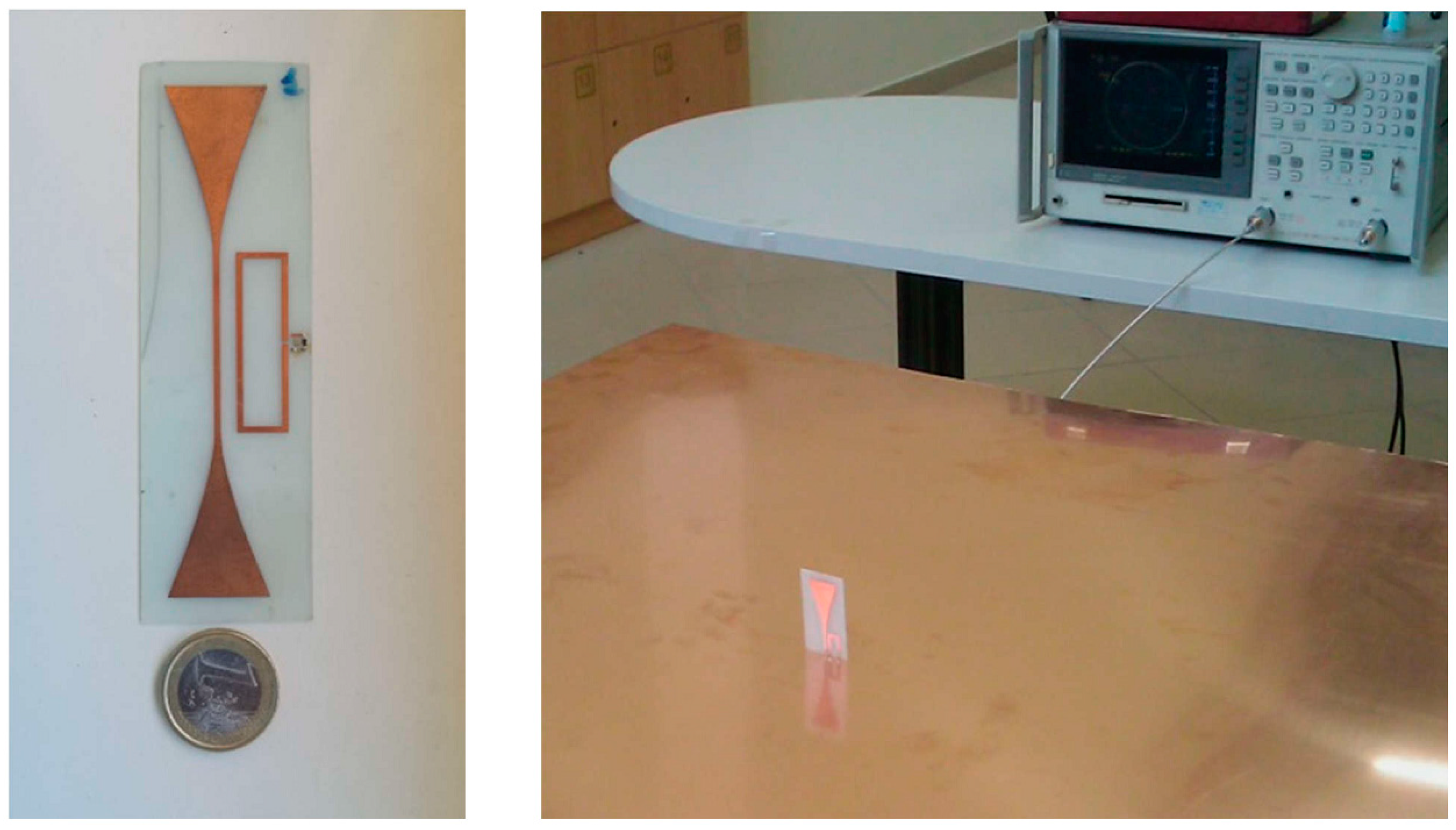
Figure 8 (left) shows the antenna prototype we realized. The measurement of the input impedance is a quite critical step due to the symmetrical input port, which should require a balun to connect it with the coaxial cable of the network analyzer, and due to the high mismatch of the antenna impedance with standard 50 Ω components. One effective solution to mitigate these problems is the set-up shown in
Figure 8 (right). Thanks to the antenna symmetry, we just used a half of the antenna placed on a
1mx
1m copper ground plane [
7]. The antenna was connected to the network analyzer through a coaxial cable placed on the other side of the copper plane. The measured input impedance and power transfer coefficient are compared with simulation results in
Figure 6 and
Figure 7 showing a good agreement. The reduction of the experimental value of the power transfer coefficient at 900 MHz is due to the higher prototype antenna resistance with respect to the numerical design.
Figure 7.
The measured (solid line) and simulated (dashed line) power transfer coefficient between antenna and chip.
Figure 7.
The measured (solid line) and simulated (dashed line) power transfer coefficient between antenna and chip.
Figure 8.
Antenna prototype (left) and antenna input impedance measurement set-up (right).
Figure 8.
Antenna prototype (left) and antenna input impedance measurement set-up (right).
3. Realization and Characterization Results of the IC Converter
The integrated circuit implementing the RF-DC converter and the Smart Voltage Regulator has been realized in STM 130 um technology. The chip area is of 550 × 400 µm2.
We characterized the performances of the RF-DC converter including the smart voltage regulator by measuring the output voltage and the converter efficiency. Such measurements have required an
ad hoc measurement setup because of the following reasons: (i) the network analyzer and all the RF instrumentation is single-ended, thus mandating the adoption of a balun for the single-ended to differential conversion; (ii) the characteristic input impedance of the RF instruments, 50 Ω, requires one to be to matched the input impedance of the differential RF-DC converter for an accurate measurement. In order to overcome the above issues, we implemented a dedicated measurement setup for the characterization of the differential RF-DC converter, which is schematized in
Figure 9. The setup is comprised of a Network Analyzer, which emulates a 50 Ω single-ended antenna and allows for measuring the reflection coefficient
S11, the PCB Balun and the PCB testing board embedding both the converter and the matching network required to match the 50 Ω output impedance of the Balun with the input impedance of the converter. A 1.5 dB insertion loss has been considered to account for interconnections and cables.
Figure 9.
Measurement setup developed for the characterization of the differential RF-DC converter. It is comprised of a Network Analyzer, a PCB BalUn and a PCB test board embedding the Matching Network and the chip under test. Bonding parasitics have been taken into account in the design of the Matching Network.
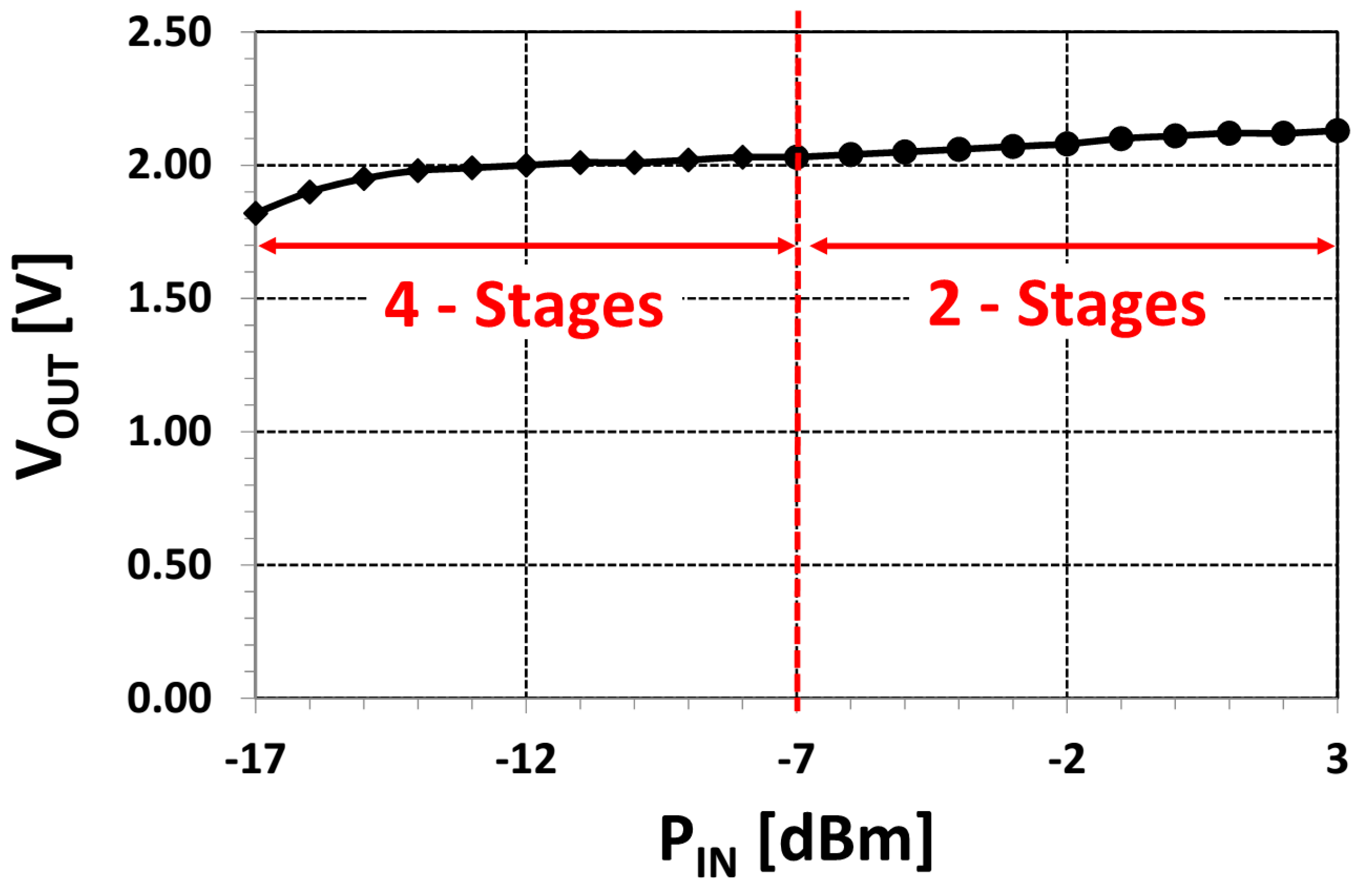
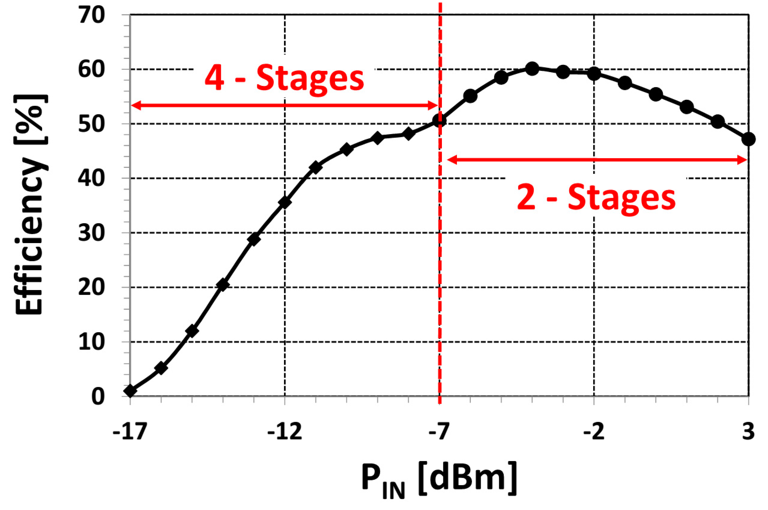
Figure 10 shows the output voltage measured at different input power level, which is around the reference voltage of ~2 V for the whole ~20 dB
PIN range. The converter starts working at −17 dBm, demonstrating a very high sensitivity. The IC efficiency calculated over the whole
PIN range peaks at 60%, while remaining above 40% over a 14 dB input power range. The above performances, among the highest ones reported in the literature, are adapted from [
13] and prove the effectiveness of the reconfigurable architecture proposed for the differential converter.
Figure 10.
Output voltage (up) and converter efficiency (down) measured at different input power levels, PIN, at 869 MHz. Similar results have been obtained at 915 MHz.
Figure 10.
Output voltage (up) and converter efficiency (down) measured at different input power levels, PIN, at 869 MHz. Similar results have been obtained at 915 MHz.
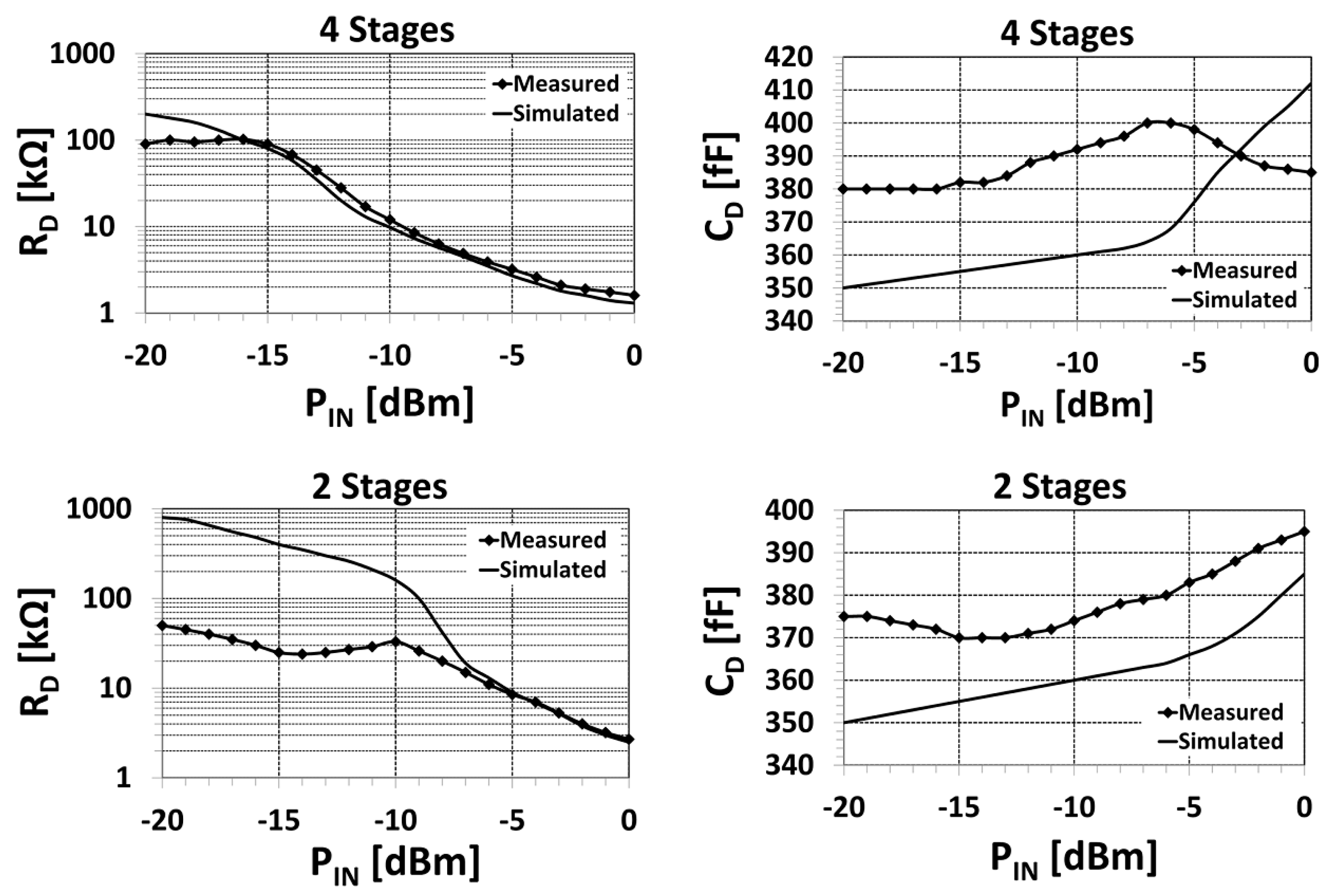
In order to properly design the antenna, we measured also the input impedance of the RF-DC converter. The differential resistance and capacitance measured at the voltage rectifier input are shown in
Figure 11 for both two-stage and the four-stage configurations. The contribution of the Balun and the PCB matching network have been de-embedded to improve the measurement accuracy. Simulations show a good agreement with measurements, except for
RD measured at input power level lower than −10 dBm.
Figure 11.
Comparison between simulated and measured input impedance (i.e., RD//CD) of the differential voltage rectifier. The input impedance is compared both for the parallel (two-stage) and series (four-stage) connection of the RF-DC Converter basic blocks.
Figure 11.
Comparison between simulated and measured input impedance (i.e., RD//CD) of the differential voltage rectifier. The input impedance is compared both for the parallel (two-stage) and series (four-stage) connection of the RF-DC Converter basic blocks.
The discrepancies of the simulated and measured input RD of the RF-DC converter are due to inaccuracy of the instrumentation for high values of RD. The reason of this inaccuracy is due to the fact that a high RD determines a |S11| dB measured with the Network Analyzer around 0 dB, and, in this condition, the Network Analyzer is less accurate.
In more detail, the inaccuracies are mainly due to the complex measurement setup we have been forced to use (see
Figure 9). From one side, all the available instrumentations are single ended and adapted to 50 Ohm. From the other side, the RF-DC converter is differential and its input impedance is not 50 Ohm and it varies accordingly with the available RF input power and the specific configuration (two-stage or four-stage). Consequently, in order to characterize the input impedance of the RF-DC converter measuring the
S11 parameter by means of a standard Network Analyzer, we had to insert a PCB balun for the single ended to differential adaption. Moreover, we also needed a tunable matching network between the balun and the RF-DC converter.
The above measurements of the rectifier input impedance were used for the design of the custom PCB antenna.
4. Realization and Characterization Results of the Whole RF Harvester System
The converter chip has been mounted on the PCB antenna realized on a FR4 substrate, while the external control logic has been implemented on a separate board.
The prototype of the whole RF energy harvester has been characterized using the experimental setup used illustrated in
Figure 12, which was developed to emulate the standard working conditions occurring in real outdoor scenarios.
Figure 12.
Setup used for the characterization of the whole system. Absorbing cones have been added to reduce the influence of reflected waves. The output current of the Smart Voltage Regulator has been measured by means of a digital multimeter in series.
Figure 12.
Setup used for the characterization of the whole system. Absorbing cones have been added to reduce the influence of reflected waves. The output current of the Smart Voltage Regulator has been measured by means of a digital multimeter in series.
The RF power signal, generated using a N5181A MXG signal generator from Agilent Technologies, is delivered to the RF energy harvesting module through a commercial broadband log-periodic transmitting antenna with linear polarization. The aligned antenna and RF energy harvester system were positioned in the maximum link direction at a distance d = 1.5 m. Their height from the soil was h = 1.8 m. A digital multimeter measured the output current of the harvester, i.e., the output of the Smart Voltage Regulator that maintains the output of the rectifier at 2 V modulating the rectifier output current. The losses due to the RF cables were de-embedded.
The characterization of the system was primarily focused on the evaluation of the energy harvesting efficiency, η, of the whole system
where
POUT is the power measured at the output of the RF energy harvester,
POUT =
VOUT ×
IOUT.
VOUT is the rectifier output voltage;
IOUT is the output current of the smart voltage regulator.
PIN is the power available at the input of the chip in case of perfect antenna-chip matching condition. It can be estimated indirectly from the Friis’s law [
14]:
where
PTX is the power transmitted by the RF signal generator;
gTX,
gRX are the gain functions of the transmitting and receiving antennas along the direction θ, ϕ respectively; χ the polarization loss factor; λ is the wavelength of the transmitted RF signal;
d is the distance between the transmitting antenna and the RF harvester. In the set-up, the antenna was polarization matched and aligned for maximum directional radiation and reception, thus Equation (3) reduces to:
being
GTX,
GRX the gain of the transmitting and receiving antennas, respectively, and they were separately characterized. For example, at the two frequencies compliant with regulations in force in North America and Europe (
i.e., 915 MHz and 869 MHz, respectively), the obtained gains have been
GTX = 7.9(8.2) dBi at 915(869) MHz;
GRX = 1.6(1.4) dBi at 915(869) MHz.
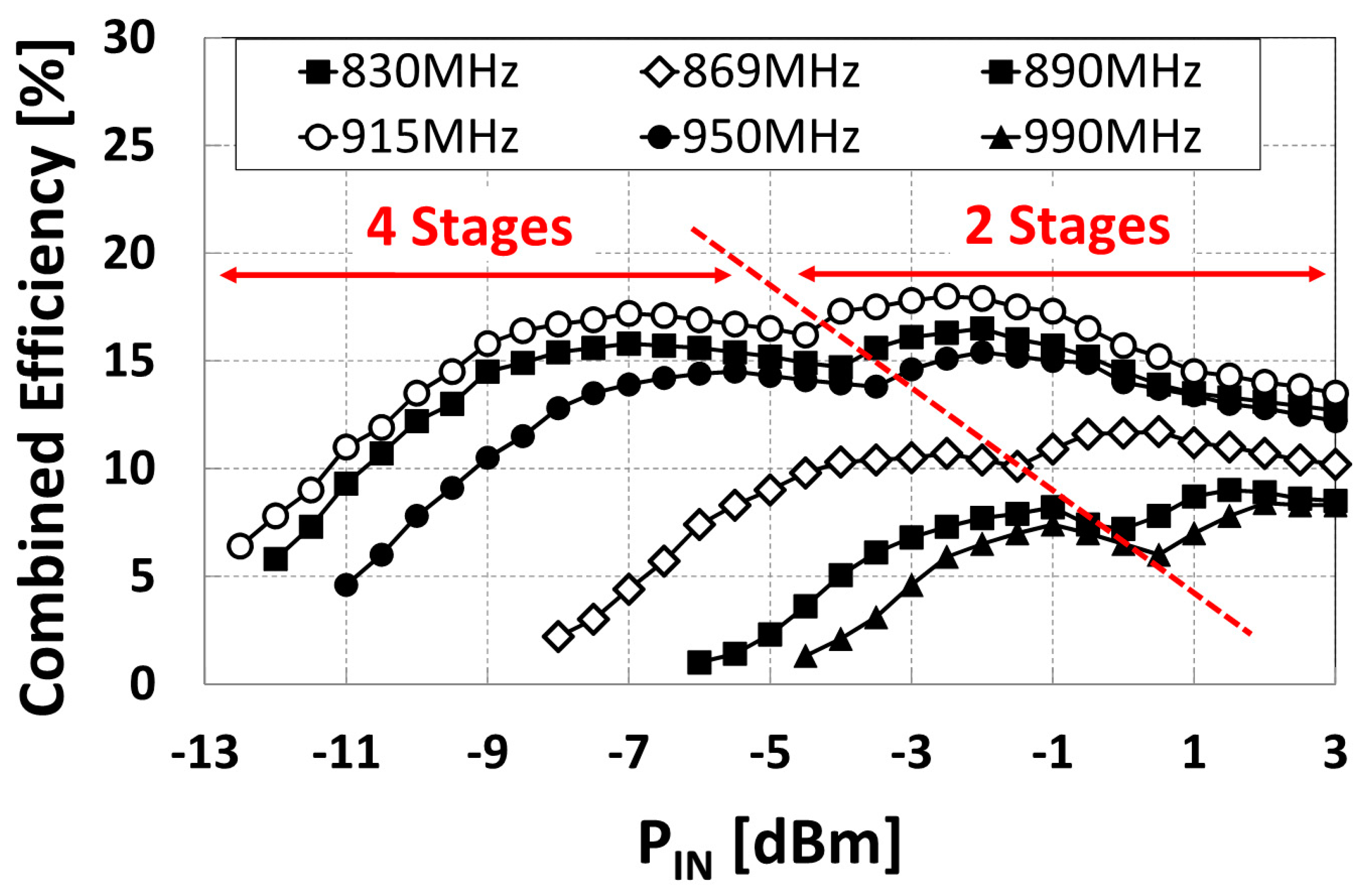
Figure 13 shows the efficiency of the whole system measured varying both the frequency and the power of the RF wave incident over the energy harvester. Efficiency curves obtained at 915 MHz and 869 MHz have been highlighted. When the series connection is selected (
i.e., four-stage configuration), the voltage rectifier shows the best sensitivity, supplying a regulated 2V output voltage starting from
PIN = −12.5 dBm (at 915 MHz). On the other hand, the parallel connection for the rectifier (
i.e., 2-stages configuration) shows the highest conversion efficiency, but it needs higher levels of
PIN to outperform the performances of the series configuration.
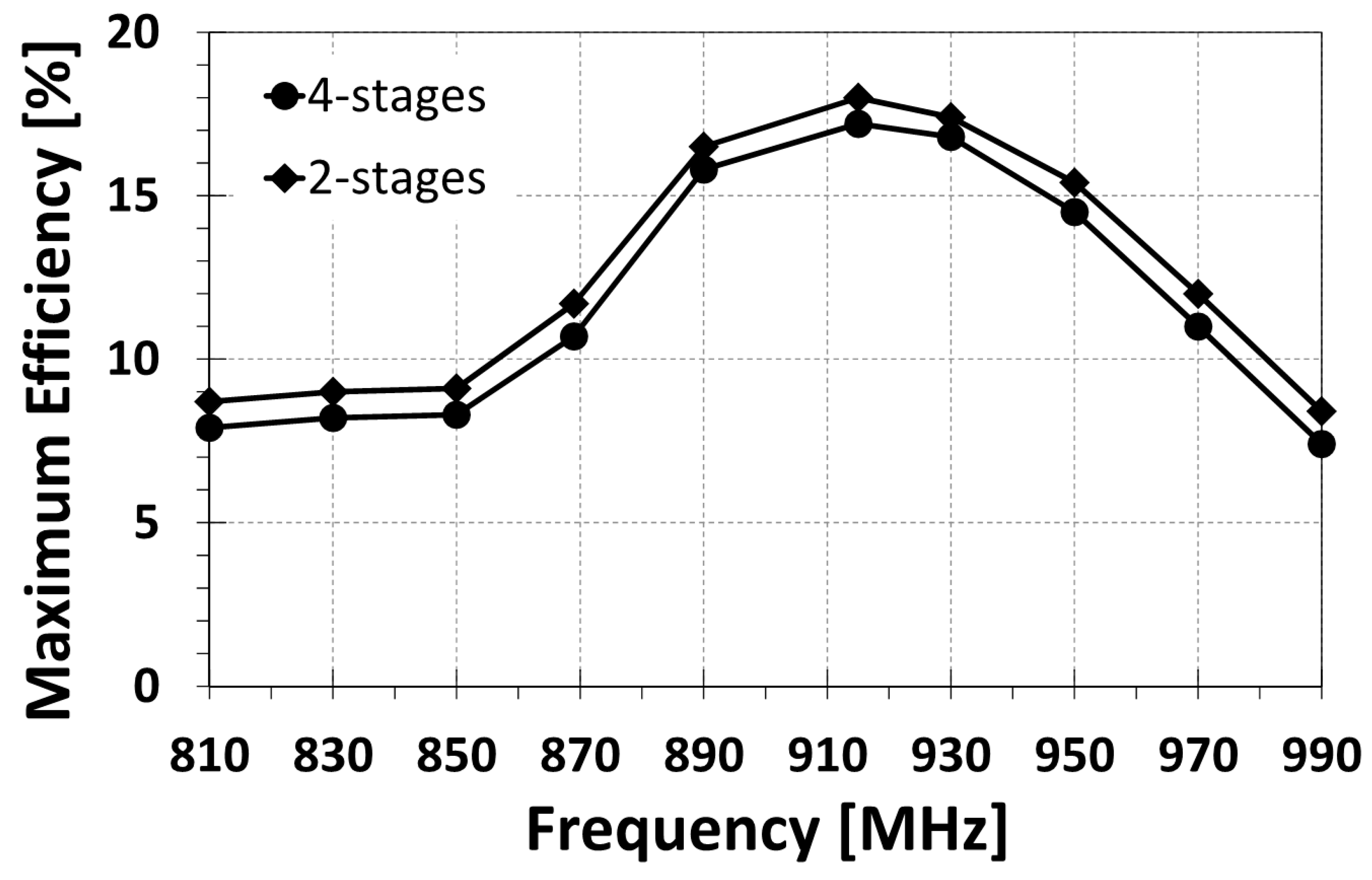
Figure 14 shows the system maximum efficiency plotted
vs. the frequency for both the series connection (
i.e., four-stage) and the parallel connection (
i.e., two-stage). Noticeably, the proposed system demonstrates an efficiency higher than 15% over a 70 MHz (55 MHz) wide-band centered at 915 MHz in case of parallel (series) connection, differing from typically narrowband RF energy harvester solutions. This is due to the implemented broadband antenna which has been designed to match the imaginary part of the chip input impedance at 900 MHz, while the real part of the antenna impedance has been chosen higher than the real part of the chip input impedance. This choice, as confirmed by the measurements, from one side allows to broaden the bandwidth as desired, on the other side does not allow to obtain the maximum power transfer at 900 MHz.
Figure 13.
Efficiency of the whole RF energy harvesting system vs. the RF input power PIN for different frequencies (not all the measured curves are shown for the sake of clarity of the figure). The frequencies compliant with regulation in force in Europe and North America are 869 MHz and 915 MHz, respectively.
Figure 14.
Maximum efficiency of RF energy harvesting system plotted vs. frequency for both four-stage and two-stage configurations.
Figure 14.
Maximum efficiency of RF energy harvesting system plotted vs. frequency for both four-stage and two-stage configurations.
The system shows a higher efficiency at 915 MHz, which is due to the better impedance matching achieved at this frequency. The reconfigurable architecture adopted for the differential rectifier benefits the efficiency, which is quite high over a large PIN range.
The main characteristics of the whole system are summarized in
Table 1, where the achieved results had been highlighted.
Table 1.
Summary of the main characteristics of the whole system.
Table 1.
Summary of the main characteristics of the whole system.
| Parameter | Value |
|---|
| RF-DC Converter Topology | Differential & Reconfigurable |
| Technology | CMOS ST130 nm |
| Output Voltage | 2.0 V |
| Sensitivity | −12.5 dBm @915 MHz |
| RF Input Power Range | 14 dB |
| Maximum Efficiency | 2-stages | 18.0% @915 MHz 11.7% @869 MHz |
| 4-stages | 17.2% @915 MHz 10.7% @869 MHz |
| Bandwidth(with η ≥ 15% and centered @915 MHz) | 2-stages | 70 MHz |
| 4-stages | 55 MHz |
| Antenna Type | Printed PCB Biconical Dipole |
| Antenna Gain | 1.6 dBi @915MHz 1.4dBi @869 MHz |
