Article

A Novel Low Power Bitcell Design Featuring Inherent SEU Prevention and Self Correction Capabilities †

1
Department of Electrical and Computer Engineering, Ben-Gurion University of the Negev, Be'er Sheva 8410501, Israel
2
Faculty of Engineering, Bar-Ilan University, Ramat Gan 5290002, Israel
*
Author to whom correspondence should be addressed.
This paper is an extended version of our paper published in IEEE S3S Conference 2014.
J. Low Power Electron. Appl. 2015, 5(2), 130-150; https://doi.org/10.3390/jlpea5020130
Submission received: 1 April 2015 / Revised: 3 June 2015 / Accepted: 8 June 2015 / Published: 23 June 2015
(This article belongs to the Special Issue Selected Papers from IEEE S3S Conference 2014)

Abstract

:
The pursuit of continuous scaling of electronic devices in the semiconductor industry has led to two unintended but significant outcomes: a rapid increase in susceptibility to radiation induced errors, and an overall rise in power consumption. Operating under low voltage to reduce power only aggravates radiation related reliability issues. The proposed “SEU Hardening Incorporating Extreme Low Power Bitcell Design” (SHIELD) addresses these two major concerns simultaneously. It is based on the concept of gating the conventional cross-coupled inverters while introducing a novel “cut-off” network. This creates redundant storage nodes and eliminates the internal feedback loop during radiation particle impact. The SHIELD bitcell tolerates upsets with charge deposits over 1 pC. Simulations confirm its advantages in terms of leakage power, with more than twofold lower leakage currents than previous solutions when operated at a 700 mV supply voltage in a 65 nm process. To validate the bitcell’s robustness, several test cases and special concerns, including multiple node upsets (MNU) and half-select, are examined.

1. Introduction

The scaling of transistor dimensions in recent years has led to an increase in power consumption, mainly due to the increase in leakage currents. Memory arrays occupy up to 70% of the die area, making memory power dissipation one of the key concerns of the semiconductor industry [1]. Low-power (LP) operation is of particular importance in VLSI chips for space applications, where available energy resources are limited. Due to the tight relationship between power consumption and voltage, one of the most attractive solutions is to scale the supply voltage. This reduces parasitic leakage currents, which define static power consumption [2]. However, low-voltage circuits are much more susceptible to radiation effects than circuits operated at nominal supply voltages.
Radiation-induced errors in electronic circuits are caused by an energy transfer when a radiation particle is knocked to the substrate, resulting in the excitement of electron-hole pairs. If the impact occurs at a transistor’s reversed biased drain junction, these carriers drift into the junction, resulting in a transient current pulse [3,4]. The prime indicator of such a single event upset (SEU) is called the “critical charge” ( Q crit ) and represents the maximal charge deposition that a node can withstand without changing its logical state. Q crit is defined as the multiplication of the node’s voltage with its capacitance (Vnode × Cnode). For this reason, lowering the supply voltage increases susceptibility to SEU [5]. Depending on the particle impact location within the chip, an overall system failure may occur.
Two main approaches have been developed to handle SEU and involve prevention and correction. At the system level, correction is typically done by Error Correction Codes (ECC) and prevention by Triple Modular Redundancy (TMR) [6]. These solutions use standard bitcell architecture and standard process and are technology independent, although they have many drawbacks in terms of additional delays and decreased efficiency related to the increased probability of multi-bit errors at small size scales [7]. At the device level, prevention is accomplished through special process techniques such as triple-well and Silicon-On-Isolator (SOI). However, these processes are expensive and do not guarantee immunity to SEU [8]. Circuit level solutions, such as DICE [9] and Quatro 10T [10], can efficiently increase SEU tolerance. Nevertheless, these solutions have flaws in the form of high power consumption and area inefficiency due to high transistor count.
Both low voltage bitcells [11,12,13,14] and radiation hardened bitcells [9,10] have been designed, but an efficient solution covering both issues is very challenging. Recently, we proposed the SHIELD bitcell [15] specifically designed for high reliability and low-power operation. It was shown that SHIELD tolerates upsets with charge deposits over 1 pC with more than twofold lower leakage currents than previous solutions when operated at a 700 mV supply voltage in a 65 nm process. In this paper, we elaborate on further research which confirms its functionality and robustnesses. In particular, a variation of the layout design for MNU avoidance is proposed, a method for reducing the minimal supply voltage by specific threshold voltage ( V T ) modifications is explored, the write speed is improved by the use of “WL boost” and the influence of “half-select” situation on the SHIELD bitcell is examined. Moreover, several test cases, such as operation in various technologies and under different supply voltages are reviewed and phase array diagrams are introduced to illustrate the bitcell’s stability.
The paper is organized as follows: In Section 2 previous related work is discussed. The proposed bitcell is discussed in Section 3. The experimental setup and results are described in Section 4. The layout design of the new bitcell is shown in Section 5. Section 6 concludes the paper.

2. Previously Proposed Radiation Hardened by Design Bitcells

In this section the two popular Radiation Hardened By Design (RHBD) bitcells, mentioned in the introduction are briefly reviewed.

2.1. DICE

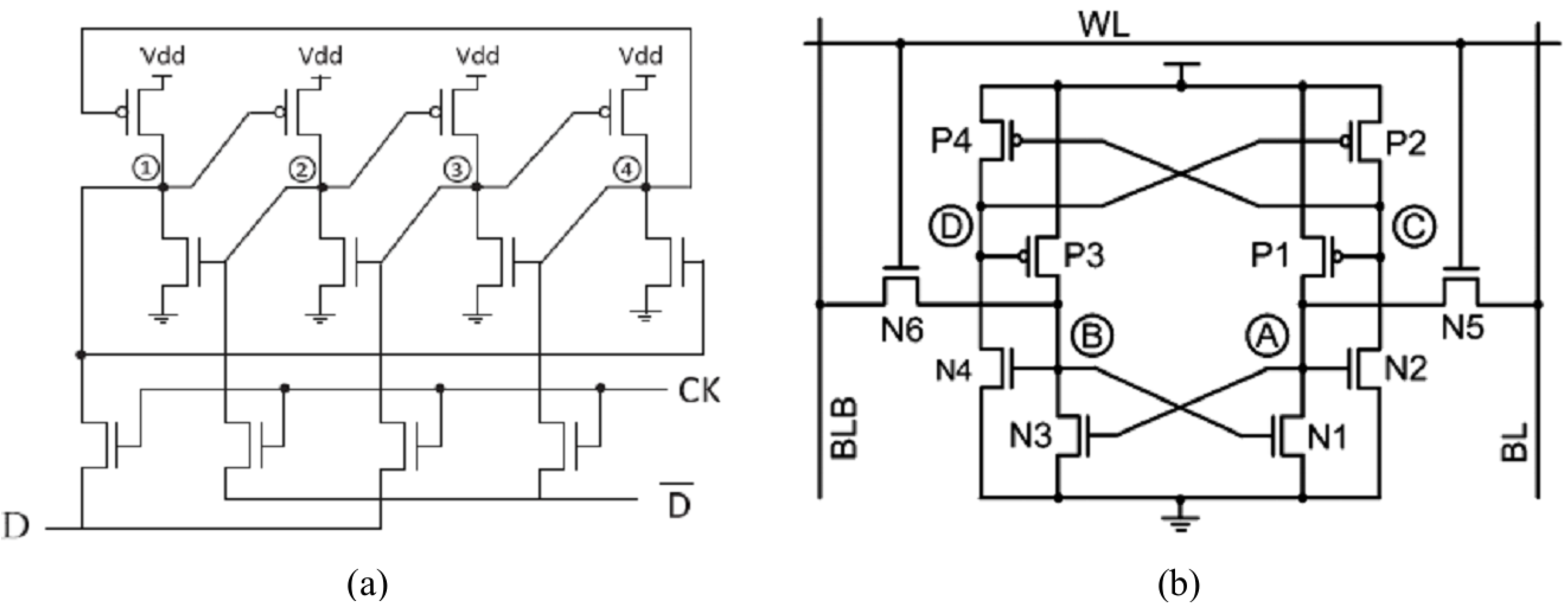
The DICE, seen in Figure 1a, uses 12 transistors and is based on a dual node feedback control methodology [9]. This means that the logic state of each of the nodes of the bitcell is controlled by two adjacent nodes. In this way a single node upset (SNU) does not propagate to the other nodes. However, its main disadvantages are its sensitivity to multi-node upset (MNU) and high power consumption because of its many transistors and leakage paths. Additionally, the DICE bitcell does not function well at low supply voltage.
Figure 1. (a) The Dice bitcell; (b) The Quatro 10T Bitcell.
Jlpea 05 00130 g001

2.2. Quatro-10T

A quad-node ten transistor soft error tolerant SRAM bitcell was presented in [10]. As seen in Figure 1b, it has two access transistors as compared to four in the DICE. This decreases the bitcell’s area and leakage current through the access transistors but significantly increases the write propagation delay. Moreover, due to its reliance on ratios, the transistors should be carefully sized to ensure correct functionality. In spite of the multiplication of the storage data nodes, the bitcell still has a sensitive node that can flip it after a radiation particle hit. Overall, the bitcell reduces the SEU rate (compared to the standard 6T SRAM bitcell) thus making it a good candidate for SEU hardening memory at sea level but it is still too sensitive for space applications.

3. The Proposed SHIELD Bitcell

In this section the proposed design is introduced, and its operation in different modes (hold, read, write) is discussed. Then, the mechanism which allows an inherent SEU hardening of the SHIELD bitcell is described.

3.1. Proposed Bitcell Structure

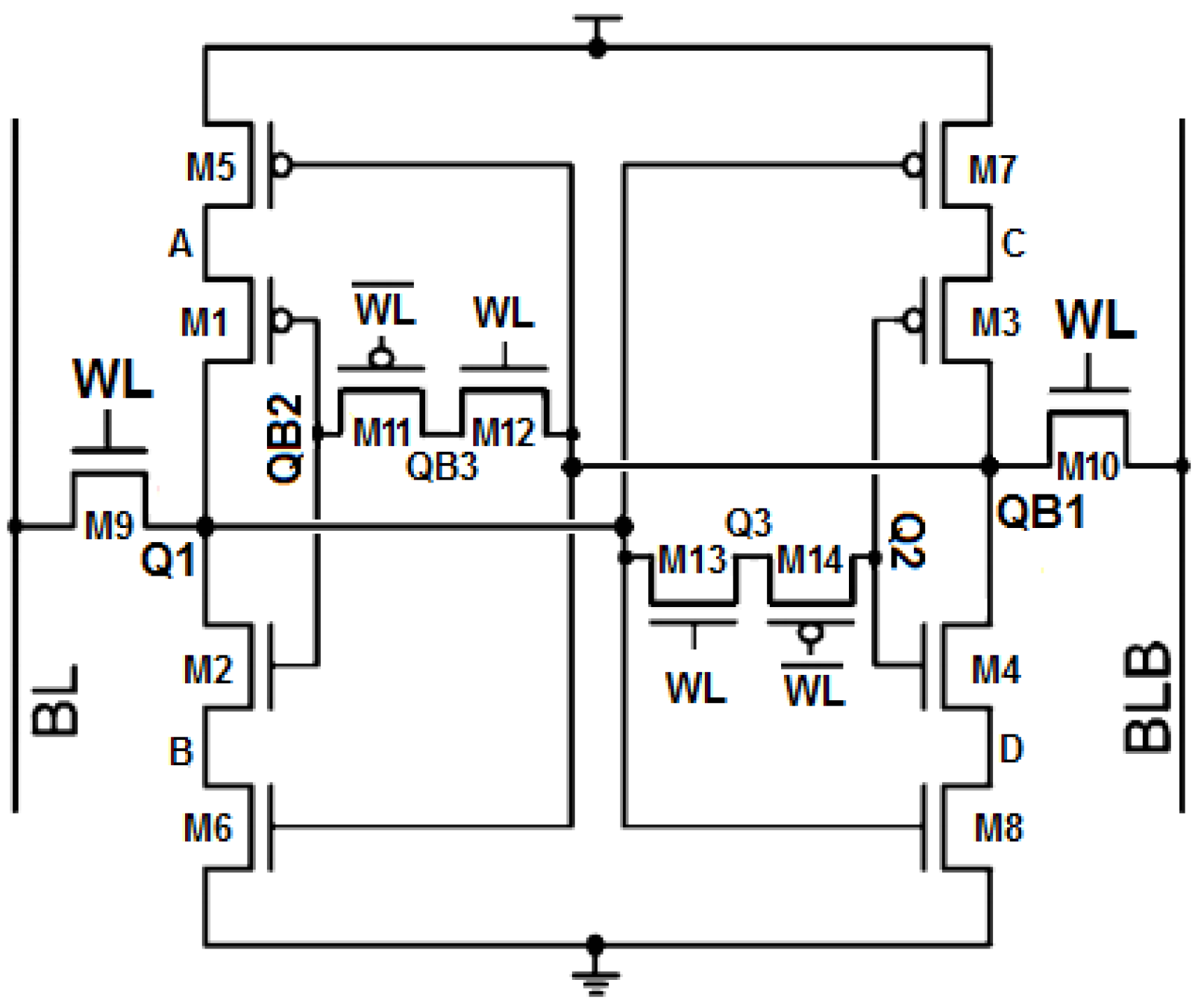
The proposed bitcell is presented in Figure 2. To mitigate SEU susceptibility, SHIELD uses gated inverters (M5-M1-M2-M6 and M7-M3-M4-M8). A gated inverter is an inverter with an additional input gate. If both inputs are in the same logical state, the output will be equivalent to that of a regular inverter. When the inputs differ from each other, the output floats with the logical state of the previous output. Novel radiation tolerant “cut-off” networks (M11-M12 and M13-M14) are connected between the two inputs of each gated inverter. This topology has two sets of separated dual data nodes ( Q 1 - Q 2 and Q B 1 - Q B 2 ). One set serves as the main data storage node and the other is for its inverted counterpart. Two additional access NMOS transistors (M9 and M10) are added for read and write purposes, as in the standard 6T SRAM. The fact that there is no need for a “read constraint” or a “write constraint” (explained in detail in the “Functionality” section), allows SHIELD to operate properly at unified minimal sizing, thus reducing its overall area and power consumption.
Figure 2. The proposed SEU Hardening Incorporating Extreme Low Power Bitcell Design (SHIELD).
Jlpea 05 00130 g002

3.2. Functionality

3.2.1. Write Operation
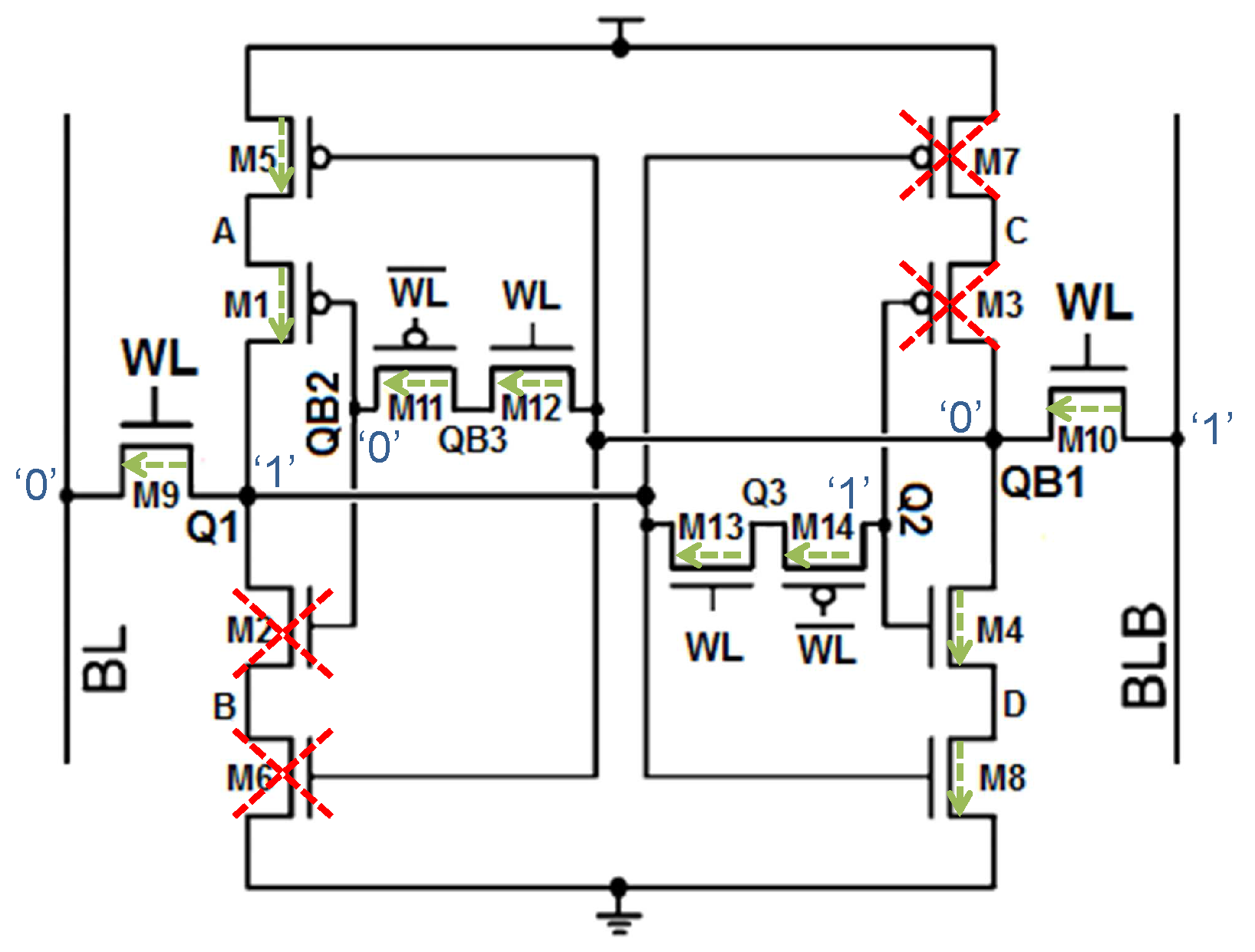
The Write operation resembles the standard 6T SRAM. It pre-charges the differential bit-lines (BL and BLB) signals to the desired data followed by the assertion of the word-line (WL) signal and its complement ( WL ¯ ). This opens the access and “cut-off” network transistors, as seen in Figure 3. After a short transient time, the voltage set at the “1” holding main data storage node ( Q 1 / Q B 1 ) is a result of the contention between the pull up network (PUN) and the access transistor. The logical state of the secondary data storage nodes ( Q 2 , Q B 2 ) is set by voltage propagation through the cut-off network, which consists of a serial NMOS and PMOS. Since NMOS does not propagate full V D D and PMOS does not propagate full GND, the logical state of the secondary data storage nodes is weaker. For symmetrical reasons, we will present write “0” operation ( Q 1 changes its state from logical “1” to “0”). Write “1” is entirely the same except that it operates on the opposite nodes. First, the BL and BLB are pre-charged to “0” and “1” respectively. While writing, WL goes to “1” and WL ¯ to “0” turning both of the ’cut-off’ network transistors and the access transistors M9 to M14 ON. We assume that the bitcell is storing a “1”, M1 and M5 are ON. After a short transient time, the voltage set to node Q 1 is the outcome of the contention between the PUN and the access transistor. The PUN must be weaker than the access transistor for the write operation to be successful. At standard 6T SRAM, this condition is met by implementing special sizing to satisfy the “write constraint”. The proposed design achieves the same outcome at minimal sizing since its PUN consists of two serially connected transistors that double its resistance path. Hence, Q 1 is pulled down lower than the voltage threshold (VM) turning M8 OFF and M7 ON. At the same time Q 2 is pulled down, turning M3 ON and M4 OFF. This results in a change in the logical state of the Q B 1 node from “0” to “1”.
Figure 3. SHIELD Write operation.
Jlpea 05 00130 g003

3.2.2. Hold State

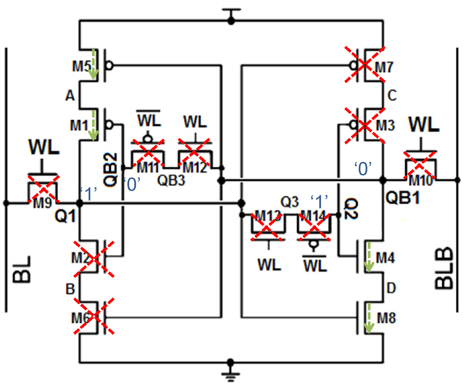
At Hold state WL = “0” and WL ¯ = “1” enclosing the data stored in Q 2 and Q B 2 , as can be seen in Figure 4. In the normal operation mode (i.e., no radiation impact), the Q 1 , Q 2 pair has the same logical state (“0” or “1”) while the Q B 1 , Q B 2 pair is in the opposite state. Note that the secondary data storage nodes are floating and their logical state is held by leakage currents as will be further elaborated at Section 3.2.4. To illustrate, let us assume the bitcell is in logical “1”. At this state, Q 1 = “1”, turns M8 ON and M7 OFF; Q 2 = “1”, turns M4 ON and M3 OFF; Q B 1 = “0”, turns M5 ON and M6 OFF and finally Q B 2 = “0”, turns M1 ON and M2 OFF. This topology results in a low resistant path from the supply rails to the data storing nodes Q 1 and Q B 1 , which allows them to replenish voltage levels to hold the stored data as seen in Figure 4.
Figure 4. SHIELD at Hold state.
Jlpea 05 00130 g004

3.2.3. Read

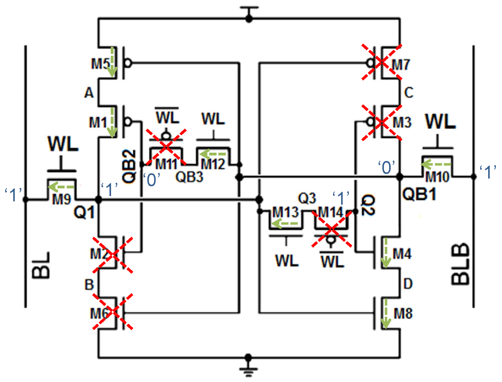
At Read operation, BL and BLB are pre-charged to V DD prior to WL assertion. A sense amplifier, connected to BL and BLB senses the voltage drop at the “0” holding node in order to determine which data the bitcell holds. The read operation can result in a bit-flip if the pull down network (PDN) is weaker than the access transistor at the “0” holding node. For a standard 6T SRAM, this condition is denied by implementing special sizing to satisfy the “read constraint”. The proposed SHIELD bitcell eliminates the need for such sizing as it is inherently protected against read bit-flips. Unlike the Write operation, for the Read operation, only the WL is asserted and not WL ¯ . This results in transistors M9, M10, M12, M13 turning ON, but M11 and M14 stay turned OFF, as seen in Figure 5. Thus, in the case where the main data storage node ( Q 1 / Q B 1 ) is flipped as a result of a read operation, the secondary data storage node ( Q 2 / Q B 2 ) will not be affected. This state resembles the aftermath of a particle impact at the main data storage node, and therefore the bitcell will recover its original state using the same built-in SEU recovery mechanisms as described in the following section. Since the NMOS transistors at the cut-off network (M12, M13) are turned ON, the median nodes ( Q 3 / Q B 3 ) exhibits charge sharing with the main data storage nodes ( Q 1 / Q B 1 ), accordingly. Read tpd is determined by the “0” holding side. This charge sharing has the effect of slowing down the read tpd, since the PDN at the “0” holding side has to pull down the extra charge, that is being accumulated at Q 3 / Q B 3 through the bitline by the access transistor (M9/M10), as well. This effect, though, is quite minor.For example, normal read tpd value at 700 mv supply voltage is 122.6 ps, whereas if M12/M13 didn’t participate in the operation and no charge sharing occurred, read tpd would be 111.5 ps.
Figure 5. SHIELD Read operation.
Jlpea 05 00130 g005

3.2.4. Behavior of the Secondary Data Storage Nodes
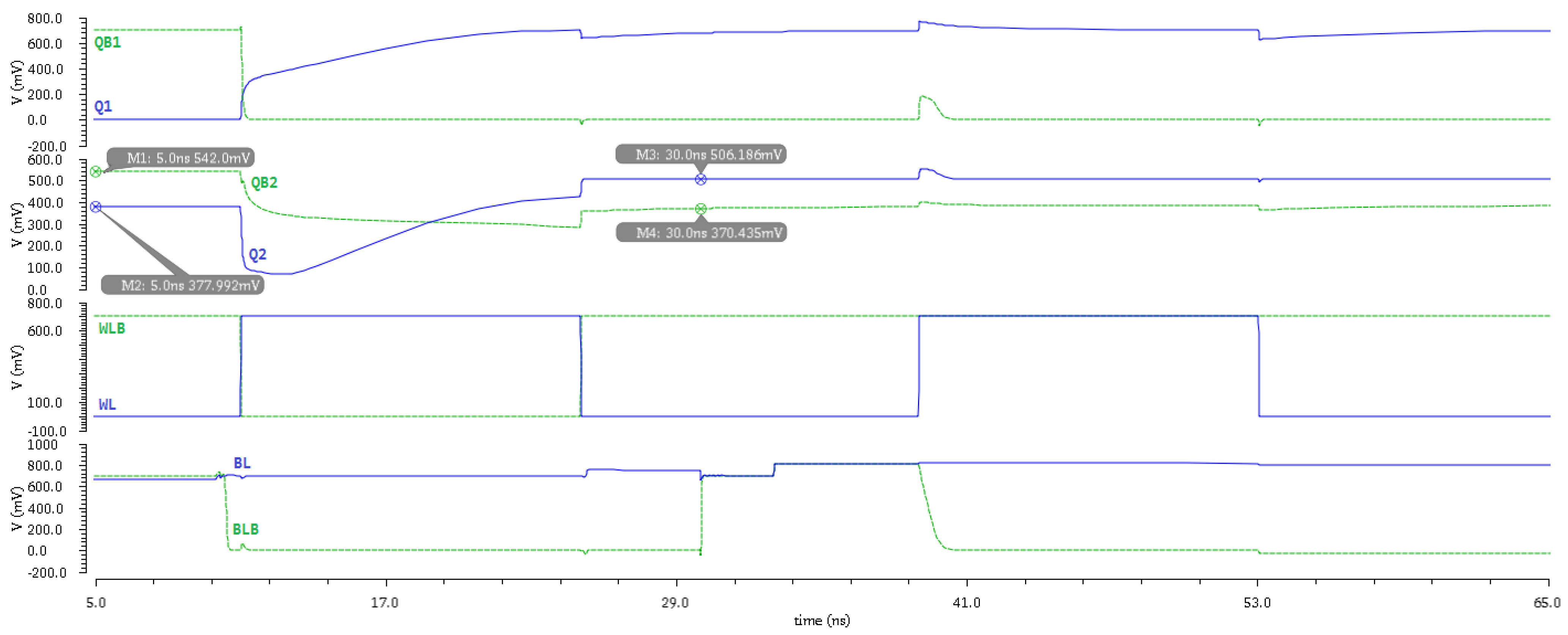
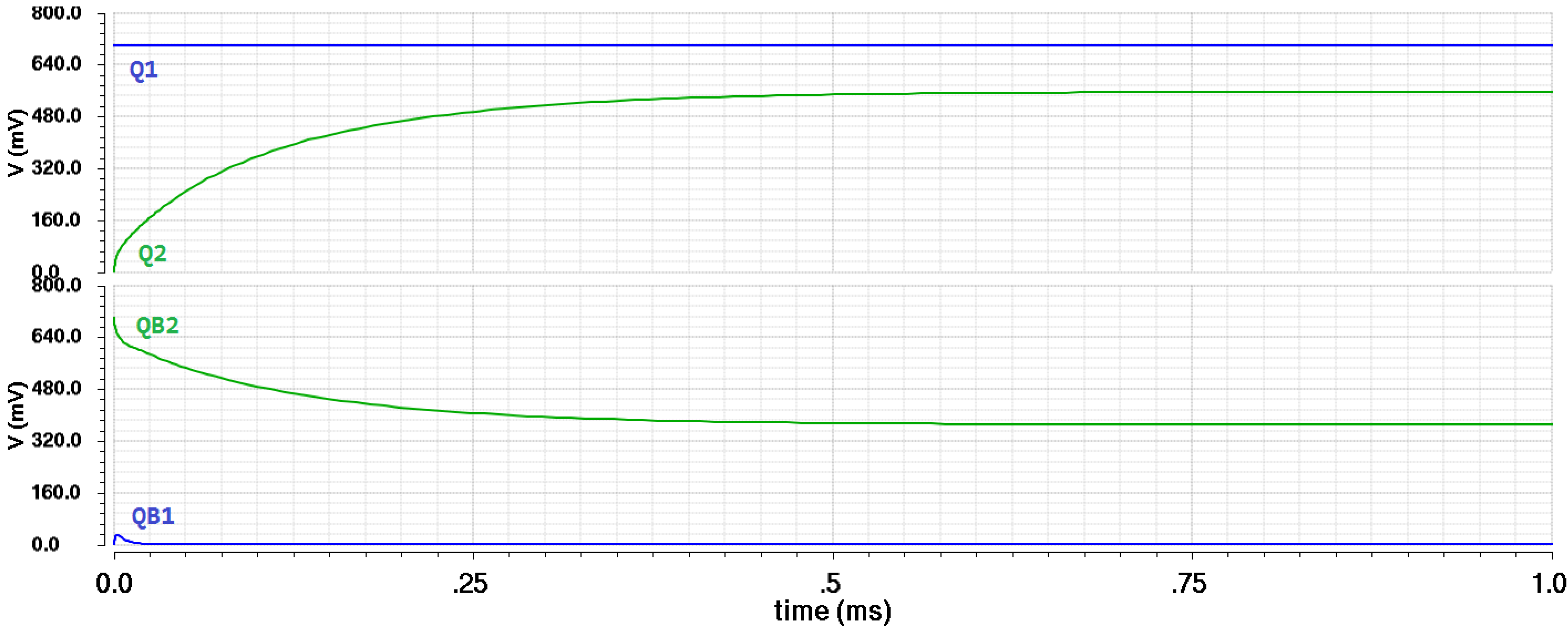
The voltage levels of the secondary data storage nodes ( Q 2 / Q B 2 ) are set during the “write” operation by propagation through the “cut-off network”, which consists of a serially connected PMOS and NMOS. The NMOS can drive voltage up to V D D V T and the PMOS can drive voltage as low as V T . Therefore, the voltage at the secondary data storage nodes can swing between V T and V D D V T . At the hold state, these nodes are floating and are held by leakage currents through the “cut-off network”. These currents are weak, since the main and secondary data storage nodes at each side holds the same logical state, resulting in low V D S equal to V T . As can be seen in Figure 6, Q 2 reaches a level of 542 mV ( V D D V T ) and Q B 2 reaches a level of 377 mV ( V T ) at hold state. Note that after WL assertion, the voltage levels of the main and secondary data storage nodes equate, before gaining the expected levels. This is due to the charge sharing effect between them.
Figure 6. Data nodes voltage during READ after WRITE sequence with supply of 700 mv.
Jlpea 05 00130 g006
The state described above is held stable while the bitcell is in “hold” state with leakage currents thorough the “cut-off” network from the main data storage node ( Q 1 / Q B 1 ) to the secondary data storage node ( Q 2 / Q B 2 ). Figure 7 shows SHIELD in “hold” state while each of the secondary data storage nodes is initialized to the opposite logical state of its complimentary main data storage node. As can be seen, the secondary data storage nodes reach their expected levels ( V D D V T and V T , respectively) by the leakage currents.
Figure 7. Secondary data storage nodes ( Q 2 , Q B 2 ) held by leakage currents.
Jlpea 05 00130 g007

3.3. SEU Hardening

This section discusses radiation particle impacts at the proposed bitcell’s sensitive nodes, and the mechanisms by which the bitcell precludes a SEU from transpiring as a result. The “cut-off” network is comprised of PMOS and NMOS devices connected in series. At Hold state both transistors of the “cut-off” network are turned OFF by external WL/ WL ¯ control signals. The impact of a radiation particle can induce negative voltage at the source of an NMOS and turn it ON even when the gate is biased GND, since V g a t e V s o u r c e = 0 V s o u r c e > V t . The same logic applies to PMOS, in that a particle impact can induce voltage levels higher than V DD at its source node and turn it ON even when the gate is biased V DD , since V s o u r c e V g a t e = V s o u r c e V DD > V t . For this reason, if the “cut-off” network had consisted of only one type of transistor, this would have made it fail at “1” → “0” radiation impact induced transitions when using a single NMOS for the “cut-off” network, and at “0” → “1” transitions when using a single PMOS. The chained formation ensures tight sealing of the “cut-off” network by assuring that when one of the transistors fails the other will stay close and a SEU transient will not permeate to the other end of the “cut-off” network. The PMOS transistor was chosen to encapsulate the secondary data storage node ( Q 2 , Q B 2 ) because it is less susceptible to radiation impact induced transients since it dwells within an N-well. Substantial part of the charge, generated at the substrate along the radiation particle track by the excitement of the electron hole pairs, is not being collected at the reverse-biased drain junction. Only charges deposited in close proximity to the junction’s immediate surroundings will be collected, while the rest will recombine, diffuse out or be collected by the bulk contact. The dimensions of this collection volume depends on the junction’s area and depth, as well as the striking particle’s track through the silicon. If this track passes through an N-well to its full depth, some of the charge will be collected by the N-well/Substrate reverse-biased PN junction instead of the drain’s. In this sense, the N-well acts as a potential barrier, limiting the collection volume by preventing charges deposited beyond the N-well boundaries from diffusing back to the struck drain junction, resulting in reduced charge collection [4,16]. An analysis of three different potentially hazardous cases at which the bitcell might exhibit a bit-flip is presented below. Due to the bitcell’s symmetry, particle impacts at Q 1 and Q 2 alone will be discussed. Impacts at Q B 1 and Q B 2 are identical, except that they operate on the opposite nodes.

3.3.1. Particle Impact at Node Q 1 from “0” to “1”

When an energized particle hits the reversed biased PMOS (M1) drain at the “0” holding Q 1 node, a current transient changes its logical state from “0” to “1”. The “cut-off” network prevents the transient from propagating over to Q 2 . The result is that M7 turns OFF and M8 turns ON. However, at the same time, M3 is turned ON and M4 is turned OFF due to the “0” stored in Q 2 . Thus, Q B 1 does not change its logical state; hence M2 and M6 remain turned ON, enabling the struck node Q 1 to replenish its original state.

3.3.2. Particle Impact at Node Q 1 from “1” to “0”

In the event of a particle hitting the reversed biased NMOS (M2) drain at the “1” holding Q 1 node, a current transient changes its state from “1” to “0”. The “cut-off” network prevents the transient from propagating over to Q 2 . the result is that M7 turns ON and M8 turns OFF. However, at the same time, M3 is turned OFF and M4 is turned ON due to the “1” stored in Q 2 . Thus Q B 1 does not change its logical state; hence M1 and M5 remain turned ON, enabling the struck node Q 1 to replenish its original state.

3.3.3. Particle Impact at Node Q 2 from “0” to “1”

Recall that Q 2 is only affected when the drain is reversed biased; i.e., the logical “0” at Q 2 as it is enclosed by a PMOS transistor. The current transient changes its state from “0” to “1”. The result is that M3 turns OFF and M4 turns ON. However, at the same time, M7 is turned ON and M8 is turned OFF due to the “0” stored in Q 1 . Thus Q B 1 does not change its logical state. While Q 2 does not have a direct path to the supply rails, it will eventually restore its original state by leakage currents through the “cut-off” network transistors M13 and M14. This process takes longer than the restoration of the main storage node Q 1 after being struck and it depends on the charge deposited, but it prevents an immediate flipping effect of the bitcell’s logical state. Read operation involves only the main data storage nodes, therefore, flipping of the secondary data storage nodes will not effect the read data. Only the combination of a strike at Q 1 when Q 2 has not sufficiently regained its logical state will result in a bit-flip. Nonetheless, the probability of the same bitcell being struck twice within this small restoration time window such that the two critical nodes change their state simultaneously are fairly low.
To illustrate the bitcell operation described in this section, representative write, read, and upset suppression events are shown in Figure 8 with the minimal operating supply voltage of 700 mV.
Figure 8. Waveform of write-strike-read operations. (blue line representing Q 1 /BL and green line representing Q B 1 /BLB).
Jlpea 05 00130 g008

4. Simulations and Results

The bitcell was simulated and compared to the standard 6T SRAM bitcell and existing circuit level radiation hardened bitcells. All the bitcells were implemented using a standard digital TSMC 65 nm CMOS technology—a 1P9M single N-well low-power process.

4.1. SEU Mitigation

4.1.1. SEU Modeling

A particle strike at a transistor’s reversed biased drain node manifests itself as fast-rising slow-establishing current interference [17]. To simulate an SEU impact on the bitcell’s sensitive nodes, a current source was connected to these nodes. The mathematical function traditionally used to portray the transfiguration of the current source over time is the double exponential current model [18]:
I t = Q τ f τ r e t τ f e t τ r
where Q is the amount of charge deposited as a result of the ion strike, which may vary with the particle hitting the node. τ r is the collection time constant, and τ f is the ion track establishment constant. For the simulations conducted here, the τ r value was set to be 45 ps, and τ f value to be 145 ps as in [18]. Q crit was calculated as the time integral over the minimum parasitic current source that causes a bit-flip. Linear energy transfer (LET) is the particle’s stopping power, which is measured in energy loss per unit path length in MeVcm 2 /mg units. It is essentially the amount of energy that an ion deposits per unit depth in a given material. The natural space environment consists of particles with varying LETs. The probability distribution of a particle drops rapidly for LET values exceeding 20 MeVcm 2 /mg to an extent where particles with LET values above 30 MeVcm 2 /mg are exceedingly rare. For this reason, a bitcell that can withstand such a particle strike at its sensitive nodes without being flipped can be considered immune to SEU [19]. To translate these values into our chosen parameter for determining a bitcell’s capability to sustain a particle hit without causing an SEU, Q crit , the following formula [20] was applied:
Q l = 1 . 6 · 10 2 · L E T · ρ E P
where Q l is the total deposited charge given in units of pC/μm, Ep is the electron-hole pair ionization energy (minimum energy required to create an electron-hole pair for a given material) given in units of eV, LET is in units of MeVcm 2 /mg, and ρ is the substrate density given in units of g/cm 3 . In the case of the commonly used silicon, Ep is 3.6 eV and ρ is 2.33 g/cm 3 , which gives values of approximately 310 fC/μm charge deposition for extremely high energy particles with a LET of 30 MeVcm 2 /mg. A value of 1 pC/ μm corresponds to the worst case scenario of particle impacts of up to 100 MeVcm 2 /mg. However, not all the charge deposited on the substrate is collected. A reversed biased node can only collect a charge from its adjacent surroundings, which extends to approximately 1 μm [4]. For this reason, we consider a bitcell with Q crit of over 1 pC as having complete SEU immunity.

4.1.2. SEU Simulation Results

Particle strike suppression according to the double-exponential model was tested in statistical Monte Carlo (MC) simulations for every type of disrupt event.
Table 1 summarizes SEU robustness of SHIELD, DICE, Quatro-10T and 6T SRAMs by measuring the Q crit values of several bitcells at a 700 mV supply voltage. The results show that the proposed SHIELD bitcell is fully immune to SEU induced in a natural space environment.
Table 1. Comparison of Q crit values.
SEU SimulationSHIELDDICEQuatro-10T6T
Q 1 :“1” →“0”>1 pC>1 pC>1 pC2.2 fC
Q 1 :“0” →“1”>1 pC>1 pC3.7 fC5.6 fC
Q 2 :“1” →“0”NP>1 pC2.5 fC-
Q 2 :“0” →“1”>1 pC>1 pC>1 pC-
Q crit >1 pC>1 pC2.5 fC2.2 fC
NP—Not Possible (Junction is not in reverse bias).

4.2. Power Consumption

Traditionally, the prime source of power dissipation has been dynamic consumption. However, as the industry has moved into sub-micron technologies, the scaling of the transistor sharply has increased the sub-threshold leakage currents, resulting in static power consumption as the dominant cause of power dissipation [21].
The SHIELD bitcell’s static power consumption value was measured and compared to the static power of the standard 6T bitcell and other existing circuit level radiation hardened bitcells. A transient simulation of 200 μs was conducted to assure all nodes at the bitcell have stabled and the leakage current has converged. Bitlines were pre-charged for the worst case scenario (voltage level opposite to those in the adjacent data node). The temperature used for simulation are nominal 25c. Higher temperature degrades minority carrier’s mobility on one hand, however at the same time it reduced V T which raises sub-threshold leakage currents exponentially with temperature. Sizing of SHIELD and 6T was set according to Section 5 and sizing criteria for DICE and Quatro 10T were set according to [9,10] respectively. Table 2 presents the leakage currents and the static power consumption comparison at a supply voltage of 700 mV.
Table 2. Power consumption and leakage current values measured at a 700 mV supply voltage.
BitcellLeakage Current [pA]Static Power [pW]
SHIELD25.3717.76
6T38.9727.28
DICE41.9329.35
Quatro 10T52.536.7
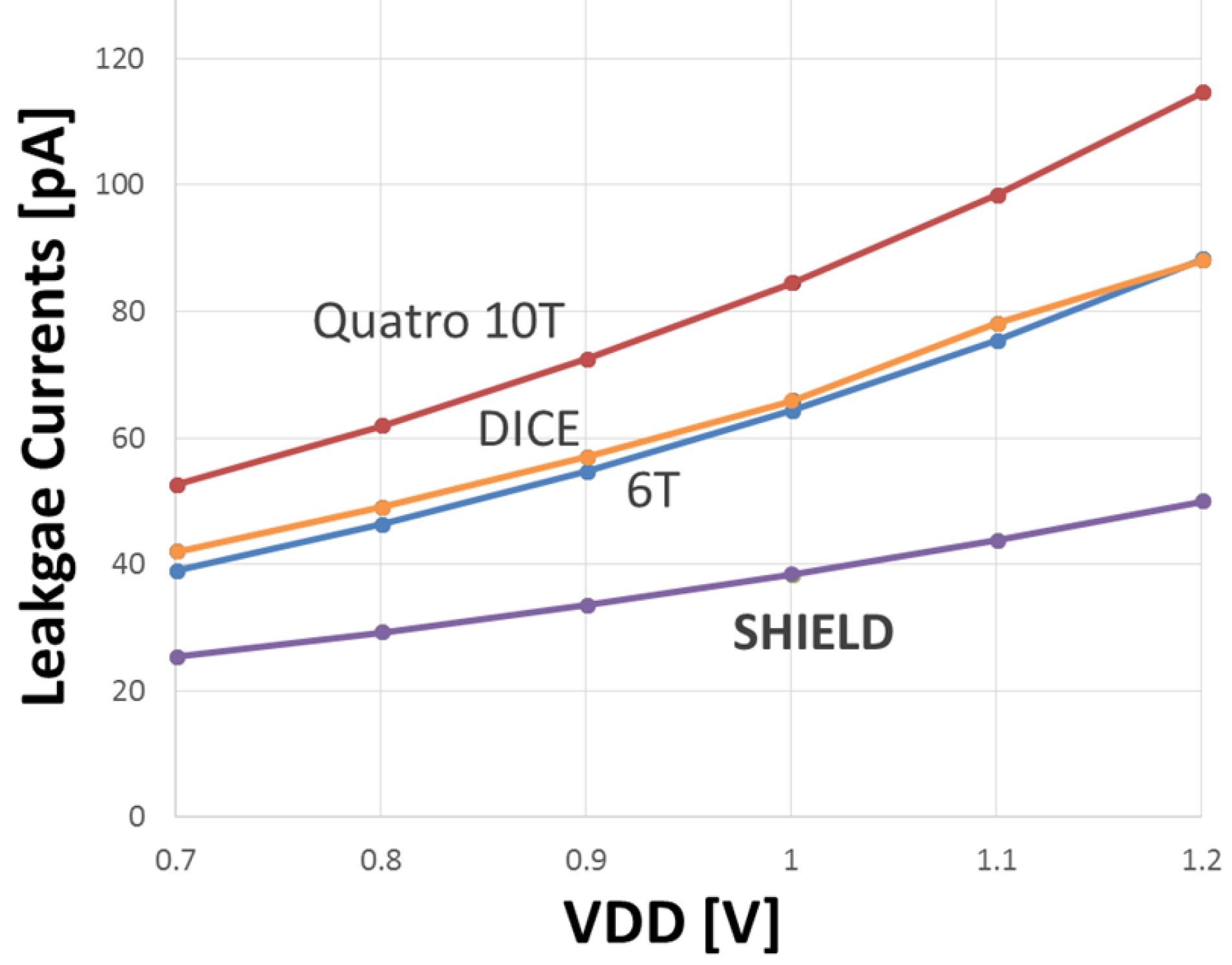
Figure 9 shows the leakage current and static power comparison between the simulated bitcells at different supply voltages.
Figure 9. Leakage currents of various bitcells as a function of supply voltage.
Jlpea 05 00130 g009
All curves represent mean values interpolated from 1000 MC samples. The findings show that the SHIELD has the lowest power consumption at all voltages. Not only does the SHIELD bitcell consumes less static power than other circuit level SEU hardened bitcells, but it also consumes less static power than the standard 6T bitcell, in spite of its high transistor count. These results stem from the use of gated inverters in the design, which provide the bitcell with internal leakage suppression capabilities through additional serial resistance in the bitcell’s leakage path to the supply rails. It should be noted, that while the DICE has the same SEU tolerance ability as SHIELD, its power consumption is higher, with values attaining 1.65 times for the DICE over SHIELD’s at 700 mV supply voltage, and more with higher supply voltages.

4.3. Improvement of Tpd

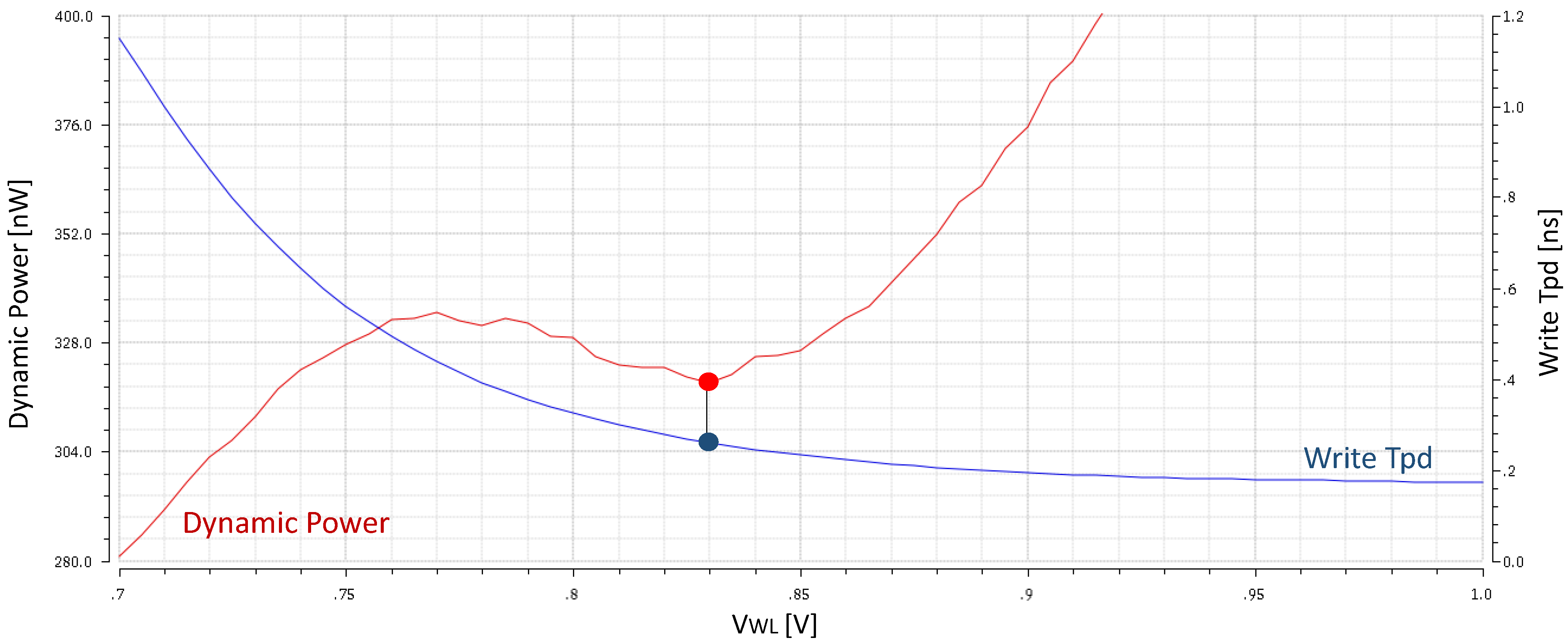
Since at write operation, SHIELD needs to drive both the main and secondary data storage nodes, the write operation suffers from higher tpd figures (1.149 ns at a 700 mV supply voltage). To ease the write operation to obtain a faster write tpd, “WL boost” was introduced to further strengthen the access transistor over the PUN. This technique raises the WL voltage beyond the regular supply voltage. While “WL boost” helps reduce write tpd, the increase in the access transistor current results in more dynamic power consumption. The simulations showed a local minimum of power consumption minimum at WL assertion of 829 mV, at which the power consumption was only 13.4% higher than that of a regular WL assertion of 700 mV (equal to the supply voltage). Write tpd reduces exponentially in such a way that beyond 0.8 V the differences can be ignored. Therefore, a sweet spot between low dynamic power consumption and fast write operation at 700 mV supply voltage exist at 829 mV boost voltage, as shown in Figure 10. At this point SHIELD reaches a write tpd of 260.9 ps, which is a 4.4× improvement in write tpd over regular WL assertion. Essentially, this solution eliminates the high write tpd concern. In addition to this improvement in performance, “WL boost” also improves the voltage levels set to the secondary data storage nodes ( Q 2 , Q B 2 ), while writing to the “1” holding node.
Figure 10. WL boost sweet spot in terms of write Tpd and dynamic power consumption.
Jlpea 05 00130 g010
The “WL boost” technique has benefits for read operation as well, as it improves the read tpd by increasing the access transistors’ driving strength. This results in a 1.55× improvement, attaining 79.16 ps Read tpd. In general, reducing the strength of the PDN in relation to the access transistor through the use of “WL boost” might result in the reduction of the cells’ stability up to the point of a read bit-flip. However, as explained in Section 4.4, SHIELD regards this situation as obsolete due to the same mechanism of SEU hardening.

4.4. Half Select Functionality

The majority of the SRAM bitcells which target low power operation suffer from susceptibility to half-select failures. Half-select situations occur during write operations when only some of the bits that share the same wordline are to be written. Usually the bitlines of the bitcells which are not written to and share the same wordline, are biased for the read operation which ensures that the bitcells will not be written to. Therefore, the read margin is often the limiting factor in supply voltage scaling of SRAM bitcells. This either leaves the bitcell susceptible to half-select failures or eliminates the option of partial row writes—a real problem if bit-interleaving is desired to minimize the probability of multiple-bit failures.
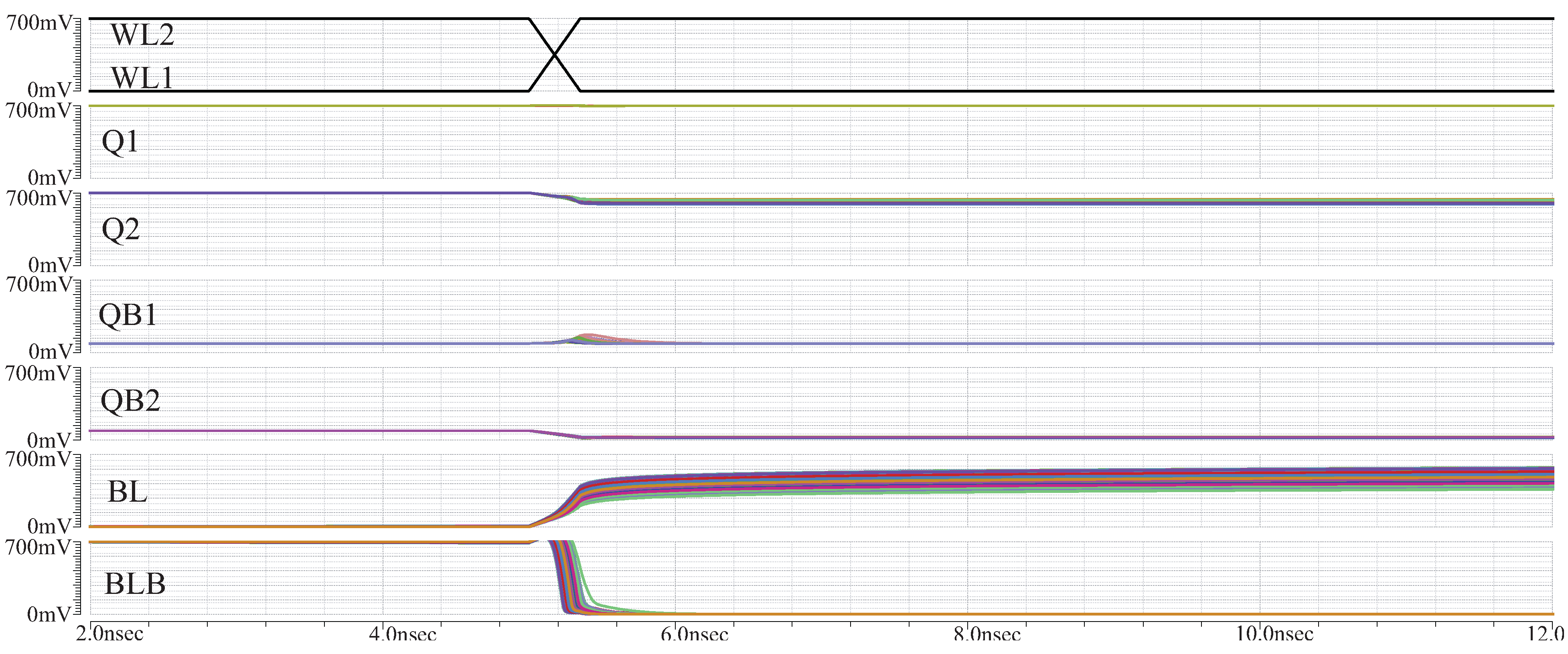
In the SHIELD bitcell, a half-select situation will indeed occur during a partial row write. However, given the strong recover mechanism of the bitcell and the indirect write operation through the cut-off network, the bitcell provides robust half-select stability. During a bit-masked write operation, the tri-state BL and BLB drivers of the non-selected cells are set to their high-impedance state, floating the bitlines. In the worst-case situation, during which the non-selected BL and BLB are driven to the opposite level than that stored in the bitcell prior to the half-select cycle, the floating charge will be discharged through Q 1 or Q B 1 without causing a bit-flip. This is shown in Figure 11 for 1000 MC samples at V DD = 700 mV. The figure depicts a bitcell in a chosen row under worst-case half-select situations. Both the BL and the BLB were initialized at the voltage opposite to that stored in the bitcell, and at the onset of a write operation (rising-edge of WL1), the BLs were floated. In all cases, only a slight disrupt was seen on the storage nodes of the bitcell, and this was quickly suppressed as the bitline charge was discharged through the mechanism of the bitcell.
Figure 11. SHIELD half select functionality.
Jlpea 05 00130 g011

4.5. Bitcell Stability

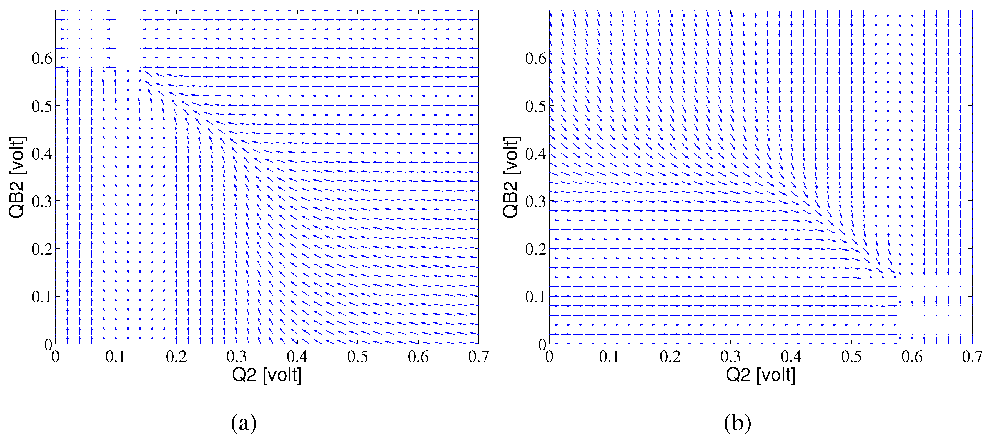
Static stability is achieved when only a single stable output state is possible for any initial condition, i.e., when all vectors converge to the same point in the state space. This is the case for both hold states (“1” or “0”) of the SHIELD bitcell, in that a set of stable points is obtained that creates a stable area. Since both main data storage nodes Q 1 and Q B 1 are held in their states by strong feedback, any disruption at these nodes will be resolved through the low resistance path to V DD or GND, unlike the case of a disruption at the secondary data storage nodes Q 2 or Q B 2 which recover through leakage currents of the “cut-off” network. To illustrate the static stability of the SHIELD bitcell during disrupts of the secondary data storage nodes, Figure 12 depicts the phase-portraits of both types of bitcell hold states (holding “0” and holding “1”) with a supply voltage of 700 mV. These plots were assembled by sampling the voltage of Q 2 and Q B 2 nodes under the assumption of any given initial value in the state space when the bitcell stores “0” (Figure 12a) and the bitcell stores “1” (Figure 12b). For example, at the “0” holding state, it can be seen that Q 2 will converge to a value of less than 150 mV and Q B 2 will converge to a value higher than 600 mV. These voltage levels are sufficient to preserve the robustness of the bitcell.
Figure 12. (a) Dynamic stability analysis of SHIELD storing “0”; (b) Dynamic stability analysis of SHIELD storing “1”.
Jlpea 05 00130 g012

4.6. Functionality under Reduced Supply Voltage

Simulation shows that at supply voltages below 700 mV SHIELD demonstrates functionality, although with reduces performance in terms of the inner inverter’s PMOS (M1/M3) which is in cut-off state. This results in a high resistance path between the main data storage node storing a “1” to the supply rails. This is due to the fact that the secondary storage nodes ( Q 2 / Q B 2 ) are floating at the hold state. To deal with this issue, two design modifications were considered:
  • “Cut-off” network transistors (M11 to M14) implementation using lvt transistors.
    The rationale behind this modification is the increase of voltage margin at the Q 2 and Q B 2 nodes, by propagating a larger voltage swing during the write operation. This guarantees that at the side holding a logic “0”, the inner inverter PMOS transistor (M1/M3) will be in cut-off state (closed) and its complementary NMOS transistor (M2/M4) will be in sub-threshold state (open).
  • Replacement of the inner transistors of the gated inverter (M1 to M4) by lvt transistors.
    The rationale behind this modification is to make the inner inverter transistors more sensitive to the voltage levels of the secondary data storage nodes ( Q 2 / Q B 2 ), at the gate of the inner inverter.
An optimization test compared the use of each of the solutions, both together and separately, under supply voltages between 500 mV and 700 mV, as shown in Table 3. The only solution (2) which uses lvt transistors at the inner inverter improved the problematic performance below 700 mV supply voltage of the PMOS of the inner inverter region. This modification translates into better bitcell stability but comes at a cost in terms of power consumption and overall layout size because lvt transistors induce higher leakage and consume more area due to DRC rules.
Table 3. Below 700 mV operation optimization.
SuggestedSupplyLeakageStaticM1/M3
ModificationsVoltage [V]Current [pA]Power [pW]PMOS state
Before modifications0.515.587.79 Cut-off
0.618.110.86 Cut-off
0.720.814.56 Sub-threshold
Solution 10.515.647.82 Cut-off
0.618.1410.88 Cut-off
0.720.8314.58 Sub-threshold
Solution 20.516.698.34 Sub-threshold
0.619.2911.57 Linear
0.722.115.47 Linear
Solutions 1 and 20.516.698.34 Sub-threshold
0.619.2911.57 Sub-threshold
0.722.115.47 Sub-threshold

4.7. Technology In-Dependency

The simulation was replicated at 90 nm and 180 nm to confirm the bitcell’s functionality in terms of SEU immunity and power consumption. As the node scales, the Q crit scales along with it, because it is linear with node capacitance, as explained in the introduction. For this reason, higher nodes are usually employed for space applications. SHIELD bitcell’s SEU immunity was preserved for these technology nodes. Table 4 show SHIELD static power consumption at various nodes. The static power consumption differs between technologies, however the same ratio of SHIELD/6T static power was preserved despite the change in supply voltages, so that it was still lower than the regular 6T standard bitcell.
Table 4. Technology in-dependency in terms of leakage current and static power consumption.
NodeBitcellLeakage Current [pA]Static Power [pW]
65 nmSHIELD25.3717.76
6T38.9727.28
90 nmSHIELD7.75.4
6T9.576.7
180 nmSHIELD2.591.82
6T3.682.57

5. Layout Design

Nowadays, it is common to harden memories by applying the system level method of triple modular redundancy (TMR) [6]. The TMR method uses three standard 6T bitcells for one bit, and adds a “voting” logic to make a majority decision as to the data stored at the triplet. The layout needed for each stored bit using TMR is inherently three times larger and requires an additional area penalty in favor of the “voting” logic. Since this is the most frequent solution in the industry, we compared SHIELD area to this solution.
In order to minimize the overall layout area, all transistors except for M5-M8 corresponded to W = 150 nm, L = 60 nm. This was done to avoid certain jog related DRC rules that bind a high minimal transistor size. Transistors M5-M8 which act as an interface to the supply rails, were minimal in size (W = 120 nm, L = 60 nm) to reduce power consumption.
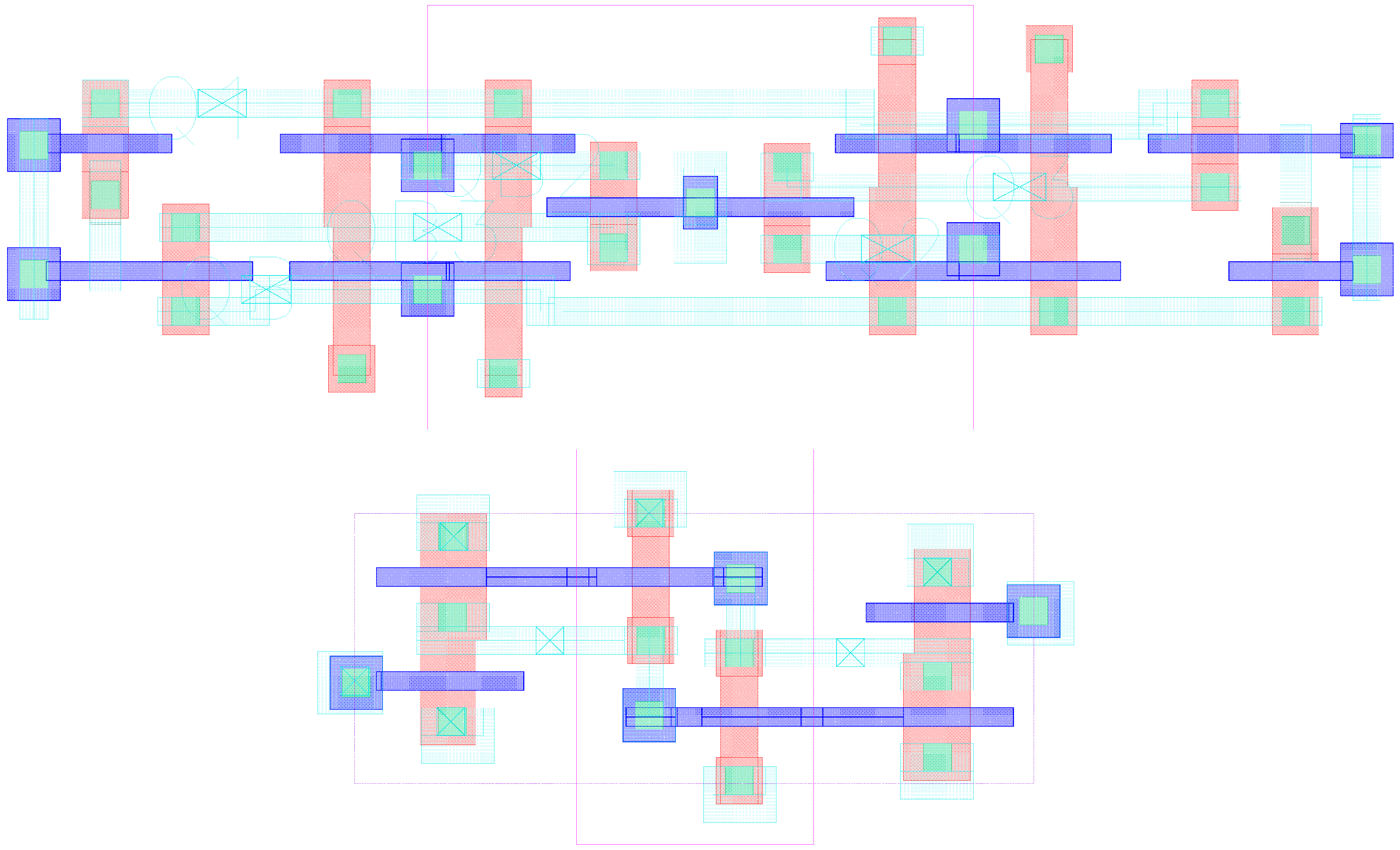
Figure 14 presents the layout design of SHIELD compared to our layout of a standard 6T bitcell. The standard 6T bitcell sizing was set according to “read constraint” and “write constraint” to be PU: W = 120 nm, L = 60 nnm, PD: W = 215 nm , L = 60 nm , PG: W = 180 nm , L = 60 nm. Full design rules were used in both implementations. Enforcing reduced design rules for SRAM implementation in both implementations could shrink the cell significantly. The proposed design achieves an area penalty of only 2.07× the standard 6T SRAM bitcell, making it extremely area efficient compared to the TMR solution.
Figure 13. Layout Design of the SHIELD bitcell (4.3 μm × 0.93 μm).
Jlpea 05 00130 g013
Figure 14. Layout Design of the SHIELD bitcell compared with the 6T SRAM bitcell (2.19 μm × 0.87 μm).
Jlpea 05 00130 g014

Layout Variation for MNU Tolerance

A charge deposited on the substrate by an energized particle diffuses and spreads out, which can result in a Multiple Node Upset (MNU). Since SHIELD reduces SEU susceptibility through redundancy, such a strike at a specific sensitive node pair ( Q 1 - Q 2 / Q B 1 - Q B 2 / Q 1 - Q B 1 ) would result in a bit-flip. According to [16], the range of possible charge sharing is about 2 μm between two NMOS transistors and 1.62 μm between two PMOS transistors in the same N-WELL given its lesser collection volume due to the N-WELL. Between NMOS and PMOS the range of possible charge sharing is only 0.6 μm as a result of the potential barrier from the P-substrate to the N-WELL. Thus, as a means of minimizing the probability of a simultaneous upset of both sensitive nodes, we devised an alternative layout design such that all sensitive PMOS-PMOS node pairs are placed in separate N-WELLs, see Figure 15. However, this solution incurs a larger area penalty. It should be noted that the larger the process, the more robust the bitcell is inherently to MNU, as the distances between the sensitive nodes increase.
Figure 15. Alternative Layout Design for MNU suppression.
Jlpea 05 00130 g015

6. Conclusions

In this paper, a novel SEU immune bitcell (SHIELD) featuring low power capabilities was proposed. Simulations showed complete immunity to SEU induced in a natural space environment. SHIELD exhibits significantly lower power characteristics than previously proposed SEU tolerant bitcells and the standard 6T bitcell. The SHIELD demonstrates functionality at a minimal supply voltage of 700 mV. This ability to operate regularly at low supply voltages and withstand radiation particle impact makes it as compatible as a low power bitcell in radiation abundant environments where energy resources are limited, such as space. Simulations demonstrated robust stability and in-dependency with the technology node. The layout design incurs an area penalty of only 2.07× compared to the standard 6T bitcell, which makes the bitcell smaller than the typical TMR solution. Future work includes the fabrication of a test chip containing the proposed bitcell memory array in standard CMOS technology and testing it under standard space radiation conditions.

Author Contributions

All authors have participates in all phases leading to the conception of this paper, and have devoted time and effort at all aspects of the paper including simulating and phrasing.

Conflicts of Interest

The authors declare no conflict of interest.

References

  1. Calhoun, B.H.; Wang, A.; Chandrakasan, A. Modeling and sizing for minimum energy operation in subthreshold circuits. IEEE J. Solid-State Circuits 2005, 40, 1778–1786. [Google Scholar] [CrossRef]
  2. Roy, K.; Mukhopadhyay, S.; Mahmoodi-Meimand, H. Leakage current mechanisms and leakage reduction techniques in deep-submicrometer CMOS circuits. IEEE Proc. 2003, 91, 305–327. [Google Scholar] [CrossRef]
  3. Messenger, G.C. Collection of charge on junction nodes from ion tracks. IEEE Trans. Nucl. Sci. 1982, 29, 2024–2031. [Google Scholar] [CrossRef]
  4. Karnik, T.; Hazucha, P. Characterization of soft errors caused by single event upsets in CMOS processes. IEEE Trans. Dependable Secur. Comput. 2004, 1, 128–143. [Google Scholar] [CrossRef]
  5. Chandra, V.; Aitken, R. Impact of technology and voltage scaling on the soft error susceptibility in nanoscale cmos. In Proceedings of the IEEE International Symposium on Defect and Fault Tolerance of VLSI Systems, Boston, MA, USA, 1–3 October 2008; pp. 114–122.
  6. Sterpone, L.; Violante, M. Analysis of the robustness of the TMR architecture in SRAM-based FPGAs. IEEE Trans. Nucl. Sci. 2005, 52, 1545–1549. [Google Scholar] [CrossRef]
  7. Chen, C.L.; Hsiao, M.Y. Error-correcting codes for semiconductor memory applications: A state-of-the-art review. IBM J. Res. Dev. 1984, 28, 124–134. [Google Scholar] [CrossRef]
  8. Schwank, J.R.; Ferlet-Cavrois, V.; Shaneyfelt, M.R.; Paillet, P.; Dodd, P.E. Radiation effects in SOI technologies. IEEE Trans. Nucl. Sci. 2003, 50, 522–538. [Google Scholar] [CrossRef]
  9. Calin, T.; Nicolaidis, M.; Velazco, R. Upset hardened memory design for submicron CMOS technology. IEEE Trans. Nucl. Sci. 1996, 43, 2874–2878. [Google Scholar] [CrossRef]
  10. Jahinuzzaman, S.M.; Rennie, D.J.; Sachdev, M. A Soft Error Tolerant 10T SRAM Bit-Cell with Differential Read Capability. IEEE Trans. Nucl. Sci. 2009, 56, 3768–3773. [Google Scholar] [CrossRef]
  11. Teman, A.; Pergament, L.; Cohen, O.; Fish, A. A Minimum Leakage Quasi-Static RAM Bitcell. J. Low Power Electron. 2011, 1, 204–218. [Google Scholar] [CrossRef]
  12. Teman, A.; Pergament, L.; Cohen, O.; Fish, A. A 250 mV 8 kb 40 nm Ultra-Low Power 9T Supply Feedback SRAM (SF-SRAM). IEEE J. Solid-State Circuits 2011, 46, 2713–2726. [Google Scholar] [CrossRef]
  13. Vaknin, A.; Yona, O.; Teman, A. A Double-Feedback 8T SRAM Bitcell for Low-Voltage Low-Leakage Operation. In Proceedings of the 2013 IEEE SOI-3D-Subthreshold Microelectronics Technology Unified Conference (S3S), Monterey, CA, USA, 7–10 October 2013; pp. 1–2.
  14. Kulkarni, J.P.; Roy, K. Ultralow-Voltage Process-Variation-Tolerant Schmitt-Trigger-Based SRAM Design. IEEE Trans. VLSI Syst. 2012, 20, 319–332. [Google Scholar] [CrossRef]
  15. Pescovsky, A.; Chertkow, O.; Atias, L.; Fish, A. SEU Hardening: Incorporating an Extreme Low Power Bitcell Design (SHIELD). In Proceedings of the SOI-3D-Subthreshold Microelectronics Technology Unified Conference (S3S), Millbrae, CA, USA, 6–9 October 2014; IEEE: Piscataway, NJ, USA; pp. 1–3.
  16. Amusan, O.A.; Witulski, A.F.; Massengill, L.W.; Bhuva, B.L. Charge Collection and Charge Sharing in a 130 nm CMOS Technology. IEEE Trans. Nucl. Sci. 2006, 53, 3253–3258. [Google Scholar] [CrossRef]
  17. Dodd, P.E.; Massengill, L.W. Basic mechanisms and modeling of single-event upset in digital microelectronics. IEEE Trans. Nucl. Sci. 2003, 50, 583–602. [Google Scholar] [CrossRef]
  18. Garg, R.; Jayakumar, N.; Khatri, S.P.; Choi, G.S. Circuit-level design approaches for radiation-hard digital electronics. IEEE Trans. VLSI Syst. 2009, 17, 781–792. [Google Scholar] [CrossRef]
  19. Hass, K.J.; Ambles, J.W. Single event transients in deep submicron CMOS. In Proceedings of the Midwest Symposium on Circuits and Systems, Las Cruces, NM, USA, 8–11 August 1999; Volume 42, pp. 122–125.
  20. Schwank, J.R.; Shaneyfelt, M.R.; Dodd, P.E. Radiation hardness assurance testing of microelectronic devices and integrated circuits: Radiation environments, physical mechanisms, and foundations for hardness assurance. IEEE Trans. Nucl. Sci. 2013, 60, 2074–2100. [Google Scholar] [CrossRef]
  21. Kim, N.S.; Austin, T.; Baauw, D.; Mudge, T.; Flautner, K.; Hu, J.S.; Irwin, M.J.; Kandemir, M.; Narayanan, V. Leakage current: Moore’s law meets static power. Computer 2003, 36, 68–75. [Google Scholar]