2. System Overview and Design
The central element of the identification system is the ID generator, a circuit that produces an N-bit ID number based on small variations in the IC due to manufacturing. The number should be random, with each bit having equal likelihood of being “0” or “1”. The random event is the manufacture of the IC, which occurs only once.
Many circuits exhibit measurable differences due to manufacturing variation that could be used to generate random, unique data. These include memories, such as SRAM power-up state [
10] and static noise margin [
11], and DRAM retention fails [
12]. Variations in delay lines and arbiters [
13], ring-oscillators [
9], scan-chain power-up state [
14], and cross-coupled inverters [
15,
16,
17], as well as direct measurements of the drain current of individual FETs [
6] have also been examined for the generation of unique identification data and PUFs.
All random ID implementations have the property that not all of the random ID bits are necessarily reliable. The ID generator circuit should produce the same ID number every time it is activated, but in such systems some bits are more reliable than others, and unreliable bits may occasionally flip between successive ID generation events. Ultimately, this could cause errors in the identification process. Current literature solves this problem by requiring each sensor to transmit its generated ID number back to the external reader, which increases the amount of data that must be transmitted. However, for such systems, wireless communication is frequently the largest energy consumer, so any reduction in transmitted data directly improves system performance. It has been observed that prior knowledge of which bits are unreliable can be used to increase the accuracy of identification [
15,
18], and that the reliability of individual bits can be determined by examining the magnitude of the underlying variation [
17].
Ideally, the ID generator bits would not be temporally random: successive reads or power-on cycles would always produce the same ID number for the lifetime of the IC. However, due to the nature of manufacturing variations and the presence of electrical noise, the value of individual bits may vary over multiple read operations. We can model the output of the ID generator, which we will call the generated code, G, as a discrete, N-bit random variable. For each bit, we can assign a probability, p, such that the probability of bit evaluating to “1” is p, and evaluating to “0” is . An N-bit ID generator can then be completely described by a sequence of N probabilities .
Based on this ID generator, each IC can then be assigned an ID code
C, where
In other words, the chip code C is the most likely value of the random variable G, the output of one read of the ID generator. It is this number that will be used to identify the IC.
2.1. Remote Identification
When an external reader attempts to locate a particular IC among a population of ICs, variations in the output of the ID generators may cause errors. For example, consider an external reader that tries to locate IC A by transmitting the chip code for chip A, . All chips in the population receive this code, and compare it to their generated codes, G. If then chip A concludes it is being addressed and can reply to the external reader. However, this may lead to false negative errors if unreliable bits in chip A’s ID generator result in .
The common way to deal with this problem is to use a slightly different approach. To find chip A in a population of M chips, an external reader transmits an inquiry to all the chips, which all reply with their generated codes, . The external reader then computes the Hamming distance between all the received codes and chip code A, for all i. The value of that has the smallest Hamming distance to is then concluded to have come from chip A.
We call this approach remote identification, since the target chip A is unable to positively conclude it is being addressed. Rather, identification happens remotely (from the perspective of the chip), at the external reader. The primary drawback of this approach is that the chip must transmit its generated code, increasing the energy consumed by the radio. This may also cause problems for systems involving large numbers of chips: some system for staggering their replies must be implemented to avoid collisions.
2.2. On-Chip Identification
By on-chip identification, we mean an addressing protocol by which chips are able to positively conclude they are being addressed. This can be accomplished with knowledge of the reliability of individual ID generator bits. Each bit of the ID generator can be classified as reliable or unreliable, based on each bit’s value of
p. Although
p is a continuous random variable, we can approximate it as a discrete random variable
, where
The variable ϵ is the threshold of reliability: reliable bits have a probability ϵ of flipping during read, and unreliable bits are treated as evaluating to either “0” or “1” with equal probability.
3. Circuit Implementation
Although there are many types of manufacturing variation that could serve as sources of entropy for a random ID generator, the type chosen for this application is the variation between the threshold voltage,
, of two identically drawn FETs. Because the variance of
is inversely proportional to the device area [
19], both devices are drawn as the minimum size available in the technology. A schematic of an
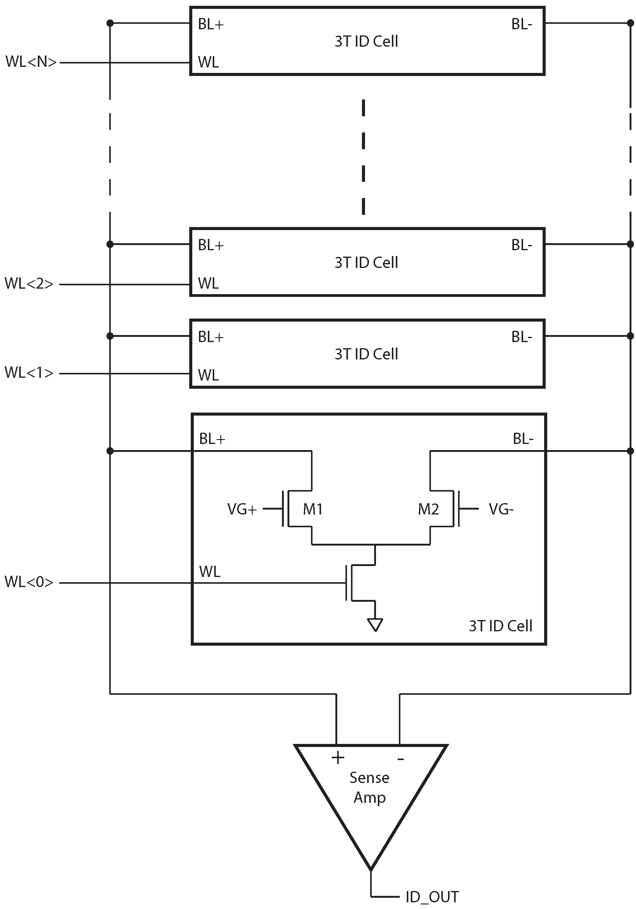
N-bit random ID generator is shown in
Figure 1.
Figure 1.
N-bit ID generator. The organization is similar to that of a memory, where multiple ID cells share a common set of bit-lines and a sense amplifier.
Figure 1.
N-bit ID generator. The organization is similar to that of a memory, where multiple ID cells share a common set of bit-lines and a sense amplifier.
The organization of the ID generator is similar to that of a memory. Each ID cell produces one random bit, based on the difference between M1 and M2. When equal gate voltages are applied to M1 and M2, the difference creates a difference in drain currents, , the polarity of which is detected by the sense amplifier (SA). A column of N ID cells is read sequentially to produce an N-bit random ID number. A simple shift register is used to drive the word-line signals rather than a row decoder, since random access is not necessary, and this requires less energy and area.
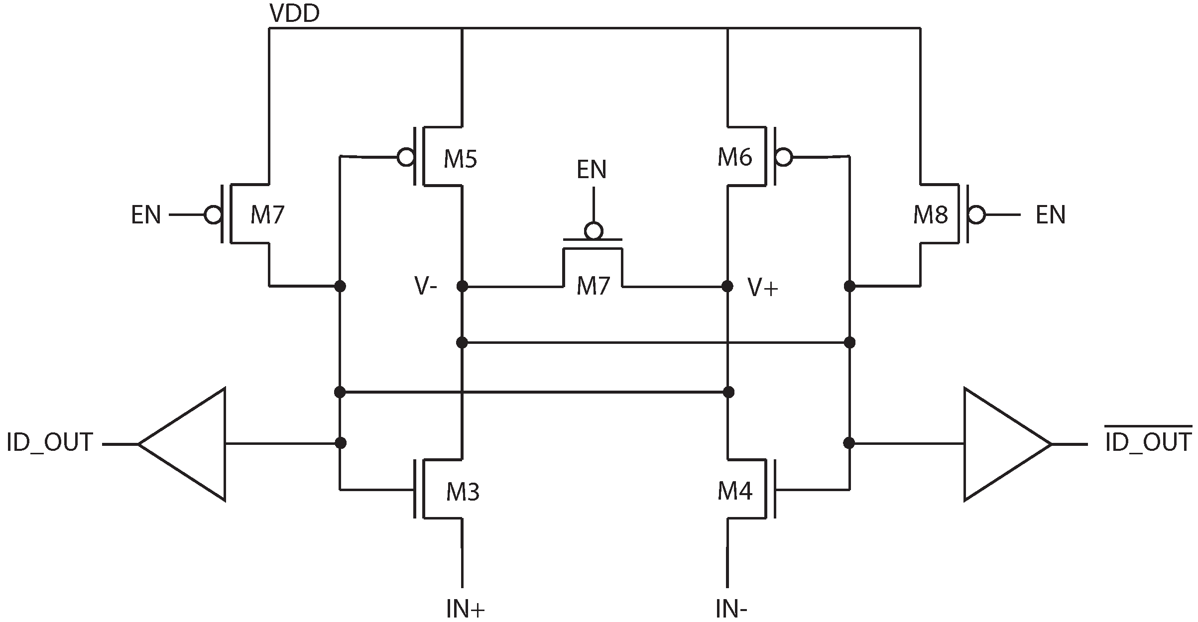
Because the SA should be constructed with negligible input referred offset, a single SA built from large devices is constructed, and shared by the column. A schematic of the latch-based sense amplifier is shown in
Figure 2. This structure is preferred for low-energy operation since it draws no static current after it has settled to its final state. Sharing the SA among multiple bits also amortizes the SA leakage current.
Figure 2.
Schematic of the latch-based sense amplifier in
Figure 1.
Figure 2.
Schematic of the latch-based sense amplifier in
Figure 1.
3.1. Noise Analysis
In the absence of electrical noise, reading from a single ID cell would be entirely deterministic. However, when the sense amplifier is activated, the total difference between the ID cell currents is the combination of the inherent offset due to device mismatch and any electrical noise, such that
The internal nodes of the sense amplifier,
and
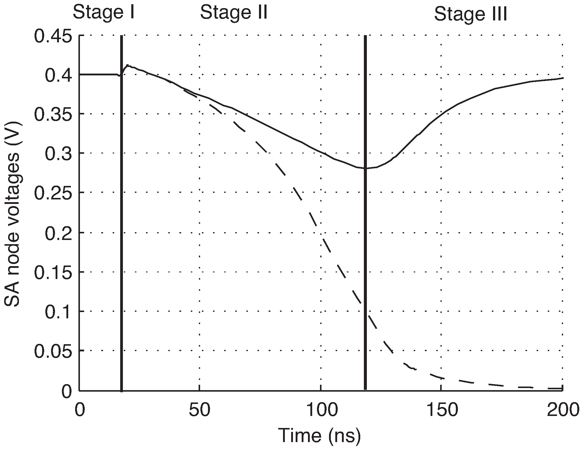
, are pre-charged to VDD prior to sensing, and devices M5 and M6 are off at the start of a read operation. When the sense amplifier is activated, the internal nodes are discharged by the ID cell current. When one of the nodes discharges sufficiently to turn on M5 or M6, the positive feedback is engaged and the amplifier settles to a stable state. A simulation of this is shown in
Figure 3, showing the three stages of operation.
The total difference voltage developed on the internal SA nodes,
, is the sum of the individual difference voltages due to mismatch and noise.
Figure 3.
Simulated operation of SA. Stage I: pre-charge, Stage II: integration, Stage III: positive feedback.
Figure 3.
Simulated operation of SA. Stage I: pre-charge, Stage II: integration, Stage III: positive feedback.
The effect of the mismatch and noise on the circuit output can be calculated. The probability of
being positive at the time the SA feedback is activated is:
This is given by:
where
is the probability density function of the normally distributed random variable
, with variance
.
Finally, this can be rewritten in terms of the equivalent input noise,
.
3.2. ID Cell Reliability
Knowing the relationship between
p and
allows for the reliability of each ID cell to be determined quickly. The magnitude of
necessary for a given reliability threshold
ϵ,
, can be calculated by inverting Equation (
9) with
.
As described in [
17], two tests can then be performed on each ID cell, first by adding a difference voltage
between the gates of M1 and M2 during read, such that
. If the result is a “0”, then
. Next, a difference voltage
is applied. If the result is a “1”, then
. The ID cell can then be classified into one of three categories: reliable “1”, reliable “0”, or unreliable, based on the two tests. The classification system is shown in
Table 1.
4. Masked Addressing
Because unreliable ID bits may lead to identification errors, some method for ensuring reliable identification is required. One obvious possibility would be to simply exclude all chips that have unreliable ID bits from use, but this would significantly reduce the yield, particularly in systems employing large numbers of ID bits.
Table 1.
Classification of ID cells based on reliability tests, where is the magnitude of the threshold voltage difference required for reliable operation, C is ID code, and M is the ID mask.
Table 1.
Classification of ID cells based on reliability tests, where is the magnitude of the threshold voltage difference required for reliable operation, C is ID code, and M is the ID mask.
| | Classification | C | M |
|---|
| True | False | “0” | 0 | 1 |
| False | False | Unreliable | X | 0 |
| False | True | “1” | 1 | 1 |
An alternative is to record which ID bits of a particular chip are reliable, and then exclude the unreliable ID bits from use during identification. This is accomplished by recording two numbers for every chip: an
N-bit ID code
C, and an
N-bit code mask
M. Each bit
is equal to “1” if the corresponding ID code bit
is reliable, and equal to “0” if
is unreliable. The values of
and
can be determined from the reliability tests as indicated in
Table 1.
To identify a particular chip
A, an external reader transmits both
and
. Every chip receives this code and activates its ID generator, which produces a generated code,
G, and then tests the following equality
If this equality is true, the chip can determine it is being addressed. Because the generated code, , will only vary from among the bits excluded by the mask, , this will ensure reliable identification. The protocols for initial chip characterization and subsequent chip identification are given below.
4.1. Chip Characterization
Chip characterization occurs once for each chip, recording
C and
M, which are necessary to identify the chip in the future.
- (1)
A single chip A, to be characterized, is placed in range of the external reader. The external reader transmits a characterize signal.
- (2)
The chip applies a voltage difference to the ID cells, activates the ID generator, and records the output .
- (3)
The chip applies a voltage difference to the ID cells, activates the ID generator, and records the output .
- (4)
The chip transmits and to the external reader.
- (5)
The external reader computes:
- (6)
The external reader stores and for chip A.
4.2. Chip Identification
Chip identification occurs when the system needs to locate a particular chip from a group of chips. Following identification, the chip can reply with a simple acknowledgement, and any other data to be collected.
- (1)
To identify chip A, the external reader transmits and . All chips within range receive this message.
- (2)
Each chip activates its ID generator, with zero voltage difference applied to the ID cells, producing a generated code G.
- (3)
Each chip evaluates the statement
- (4)
If the preceding step evaluates to true, the chip concludes it is being addressed.
4.3. Performance Metrics
An effect of this addressing scheme is that the maximum number of chips that can be addressed is reduced from the theoretical maximum of
. If only chips that have a number of unstable bits less than or equal to some maximum value,
U, are selected for use, than the maximum number of chips that can be uniquely addressed is
For a chip with
U unreliable bits, a false negative can only occur if there is an error among one of the
reliable bits. If the probability of an error in one of the reliable bits is
ϵ, then the false negative rate is
Errors among reliable bits could also cause false positive identifications. Calculating the combined probability of any false positive event is difficult, so we will restrict the calculation to single bit errors, since the probability of
E bit errors is
, which decreases rapidly for
. For
, only chips with codes within Hamming distance 1 of the target chip code can cause false positives. In the worst case, for an
N bit code with
U unreliable bits, there are
possible chip codes within a Hamming distance of 1. However, this number is usually much larger than the maximum number of uniquely addressable chips,
S, given by Equation (
15). In actual practice, therefore, there are at most
other chips that could cause false positive errors. The probability of any of these chips causing a false positive is then
The total error rate,
can then be found
Restricting the use of chips to those that have a number of unreliable bits less than or equal to
U reduces the yield. If the probability that a bit is unreliable is
, then the yield is given by
5. Experimental Results
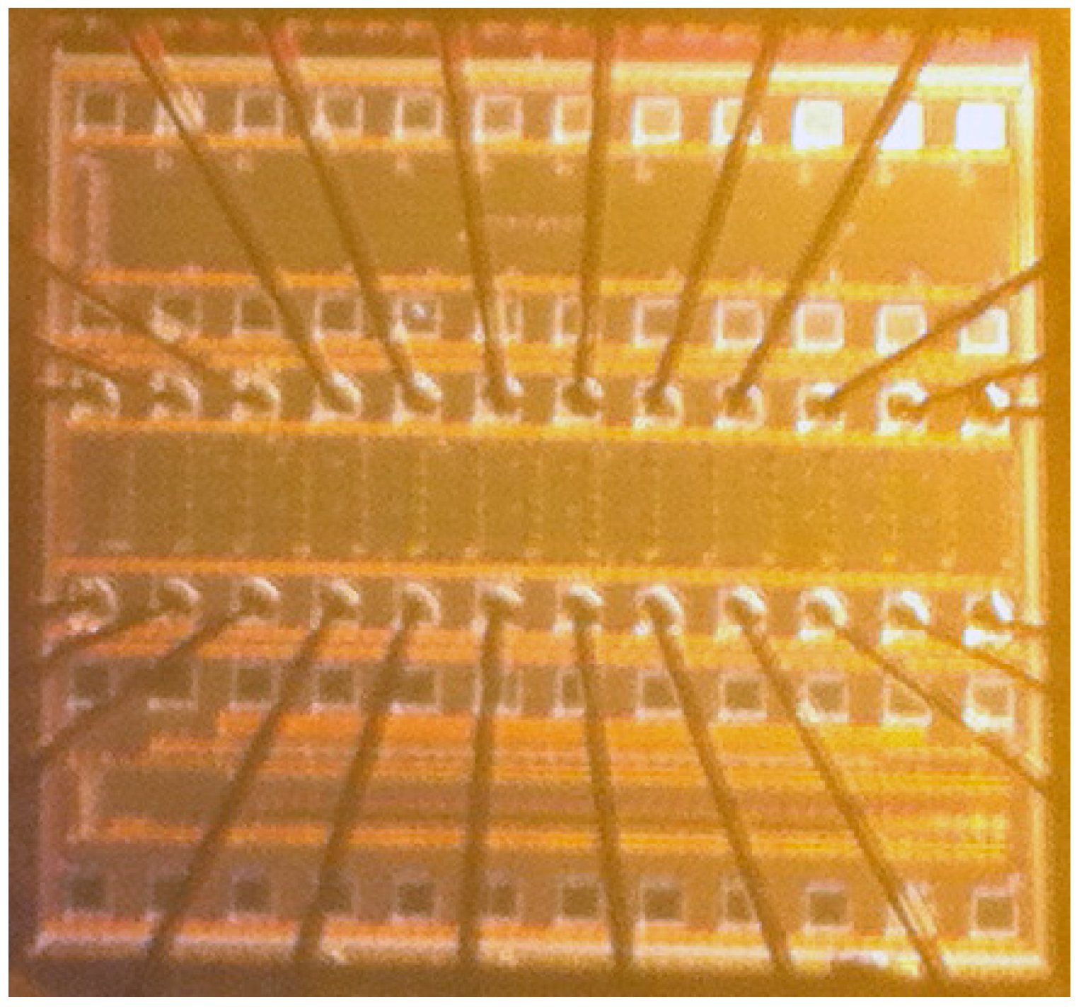
The proposed circuit was fabricated in a 130 nm CMOS process. A photograph of the manufactured die is shown in
Figure 4. As in
Figure 1, one column of ID cells shared a single SA, with 32 ID cells per column. A shift register is used to generate the row select signal, and each shift register is shared by 32 columns to for a 32 × 32 array. Fifteen of these arrays are contained on each die, for a total of 15,360 ID bits per die. One 32-bit column, including the SA, occupies an area of 68.5 × 4.3 μm. For measurement, the value of
was 400 mV.
Figure 4.
Photograph of random ID chip with 15,360 ID bits, fabricated in 130 nm CMOS process.
Figure 4.
Photograph of random ID chip with 15,360 ID bits, fabricated in 130 nm CMOS process.
For each ID cell, the value of
p was determined by reading from the cell 1000 times, and counting the number of results equal to “1”. To find the value of the threshold voltage mismatch,
in the ID cell, the gate of M1 was held fixed, and the gate of M2 was swept in 1 mV increments. At each increment, the ID cell was read 100 times. From these two measurements, the relationship between
p and
was determined, and plotted in
Figure 5. From this data, the value of the input referred voltage noise,
, was determined to be 1.5 mV.
If a reliability threshold of
is chosen, Equation (
10) indicates ID cells with
mV will behave reliably. Of the fabricated ID cells examined,
satisfy this inequality and can be classified as reliable (
). More generally,
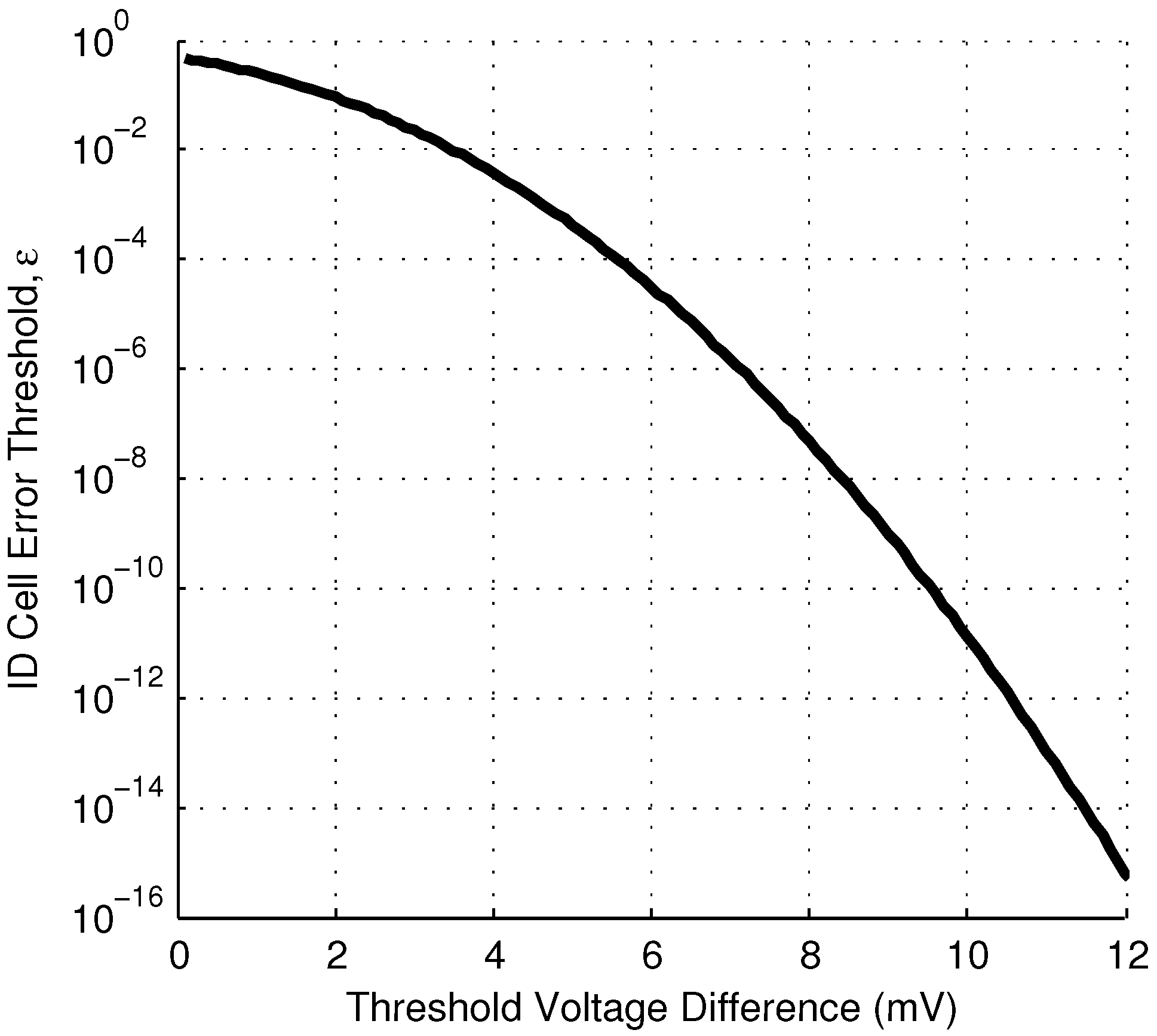
Figure 6 shows the relationship between
and the reliability threshold, and
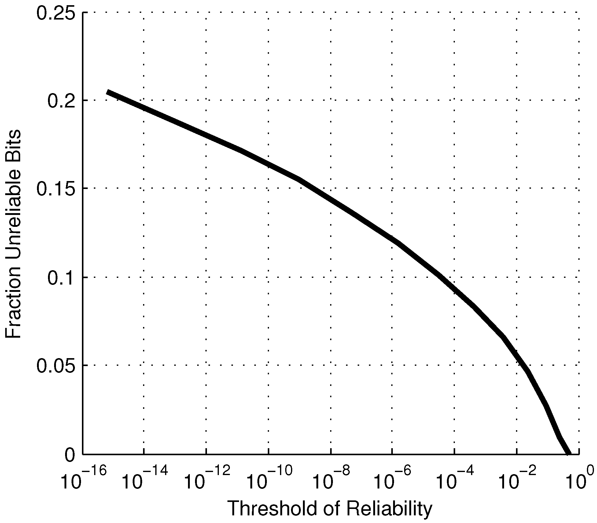
Figure 7 shows the fraction of unreliable bits for a given reliability threshold.
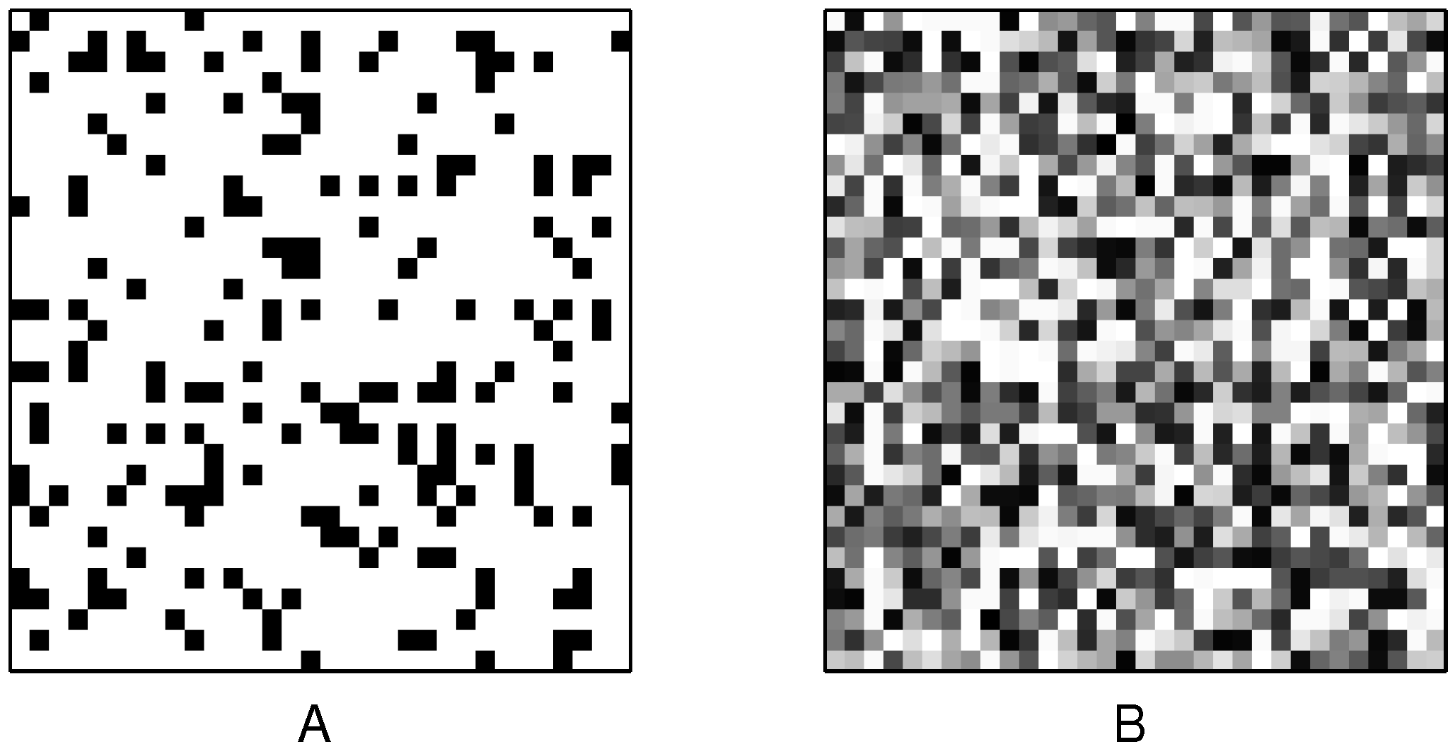
The location of unreliable cells for an arbitrarily chosen 32 × 32 array is shown in
Figure 8. The unreliable cells are shown in black. The magnitude of
is also shown for the same array. This indicates that unreliable bits have random spatial distribution in the array. The measured distribution of
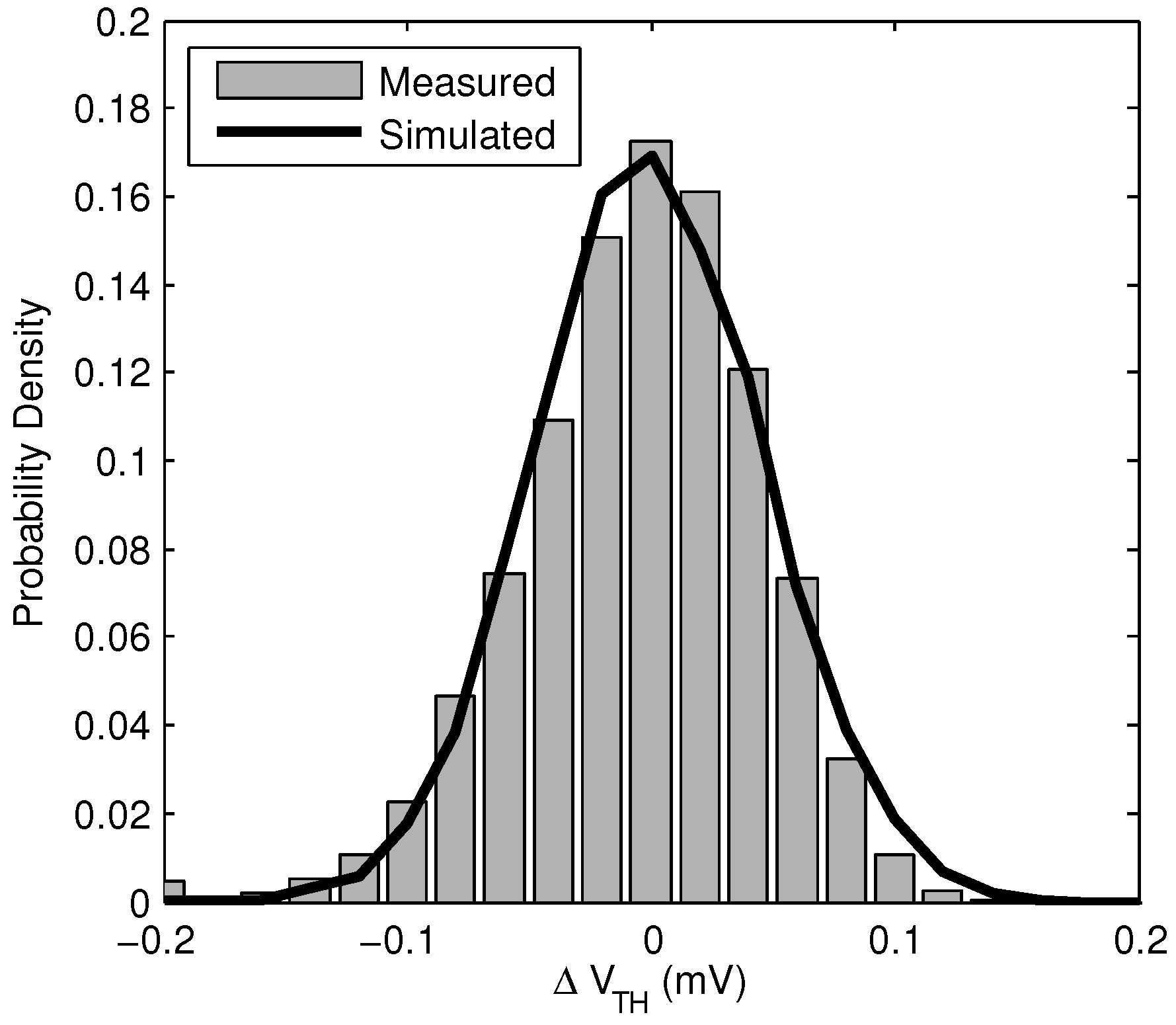
is shown in
Figure 9, along with a Monte Carlo simulation of the same distribution. This shows the distribution of
can be accurately predicted in advance for well modeled processes.
Figure 5.
Relationship of ID cell probability,
p, to threshold voltage mismatch
, measured over 15,360 bits. Equation (
9) is also plotted with
= 1.5 mV.
Figure 5.
Relationship of ID cell probability,
p, to threshold voltage mismatch
, measured over 15,360 bits. Equation (
9) is also plotted with
= 1.5 mV.
Figure 6.
Relationship between ID cell error rate, ϵ, and the magnitude of the threshold voltage mismatch in the ID cell, .
Figure 6.
Relationship between ID cell error rate, ϵ, and the magnitude of the threshold voltage mismatch in the ID cell, .
The relationship between
and the reliability threshold depends on the value of
, which will vary in different technologies. Equation (
9) shows that the required
is linearly related to
,
i.e., a 10× increase in
would require a 10× increase in the difference threshold
to maintain the same error threshold. This may reduce the yield, if the standard deviation of the threshold voltage is not also higher in the alternate technology.
The energy consumption was measured to be 39 fJ/bit at a readout rate of 40 kBps. This is 23× less than the next lowest published value of 930 fJ/bit [
16]. The decreased energy consumption is likely due to the lower supply voltage, sharing of a single SA (which amortizes the SA leakage current), and the use of a shift register for sequential access rather than a row decoder. The effective area per bit (32-bit column and sense amplifier divided by 32), is 9.2 μm
.
Figure 7.
Fraction of manufactured bits that can be expected to be unreliable for a given threshold of reliability, ϵ.
Figure 7.
Fraction of manufactured bits that can be expected to be unreliable for a given threshold of reliability, ϵ.
Figure 8.
(A) Location of unreliable bits ( mV), shown in black, in a 32 × 32 array of random ID cells. (B) Magnitude of in the same array, where black is 0 mV and white is 50 mV.
Figure 8.
(A) Location of unreliable bits ( mV), shown in black, in a 32 × 32 array of random ID cells. (B) Magnitude of in the same array, where black is 0 mV and white is 50 mV.
Figure 9.
Normalized histogram showing measured and simulated distribution of . Measured sample size is 15,360 bits, and simulated sample size is 10,000 bits.
Figure 9.
Normalized histogram showing measured and simulated distribution of . Measured sample size is 15,360 bits, and simulated sample size is 10,000 bits.
As previously noted, having a non-zero number of unreliable bits,
U, reduces the maximum number of addressable chips from the theoretical maximum of
. For this system, with
= 1.5 mV, a chosen reliability threshold of
and
, and a 99.9% yield, the maximum number of addressable chips
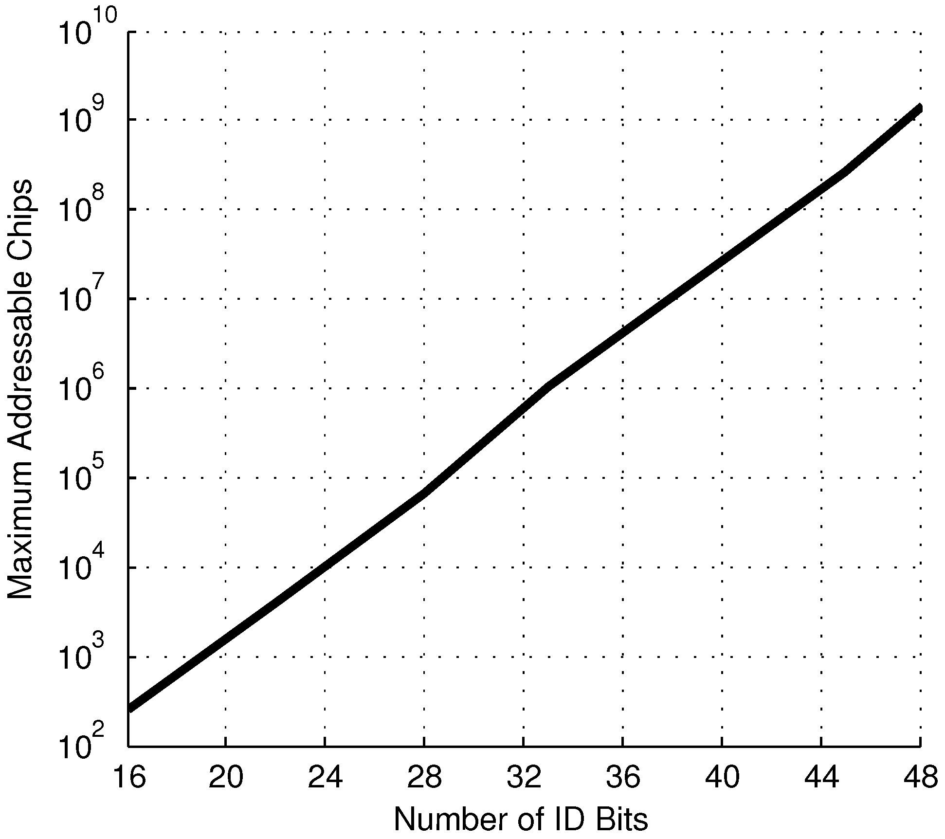
versus the number of ID bits is shown in
Figure 10. This shows reasonable performance as the addressing scheme is scaled up to large systems.
Figure 10.
Maximum number of addressable chips under the masked addressing system for a given number of random ID bits, N.
Figure 10.
Maximum number of addressable chips under the masked addressing system for a given number of random ID bits, N.
5.1. Temperature Dependence
To evaluate the reliability of the random ID system over temperature, the change in
was measured for all the ID cells over 30
C and 50
C increases in temperature. We observed that for each ID cell, the temperature dependence of
varies, in part proportionally to
, and in part randomly between cells. The change in
over the observed range is roughly linear with temperature, and so can be expressed as
where
K is a random variable, with mean value proportional to
:
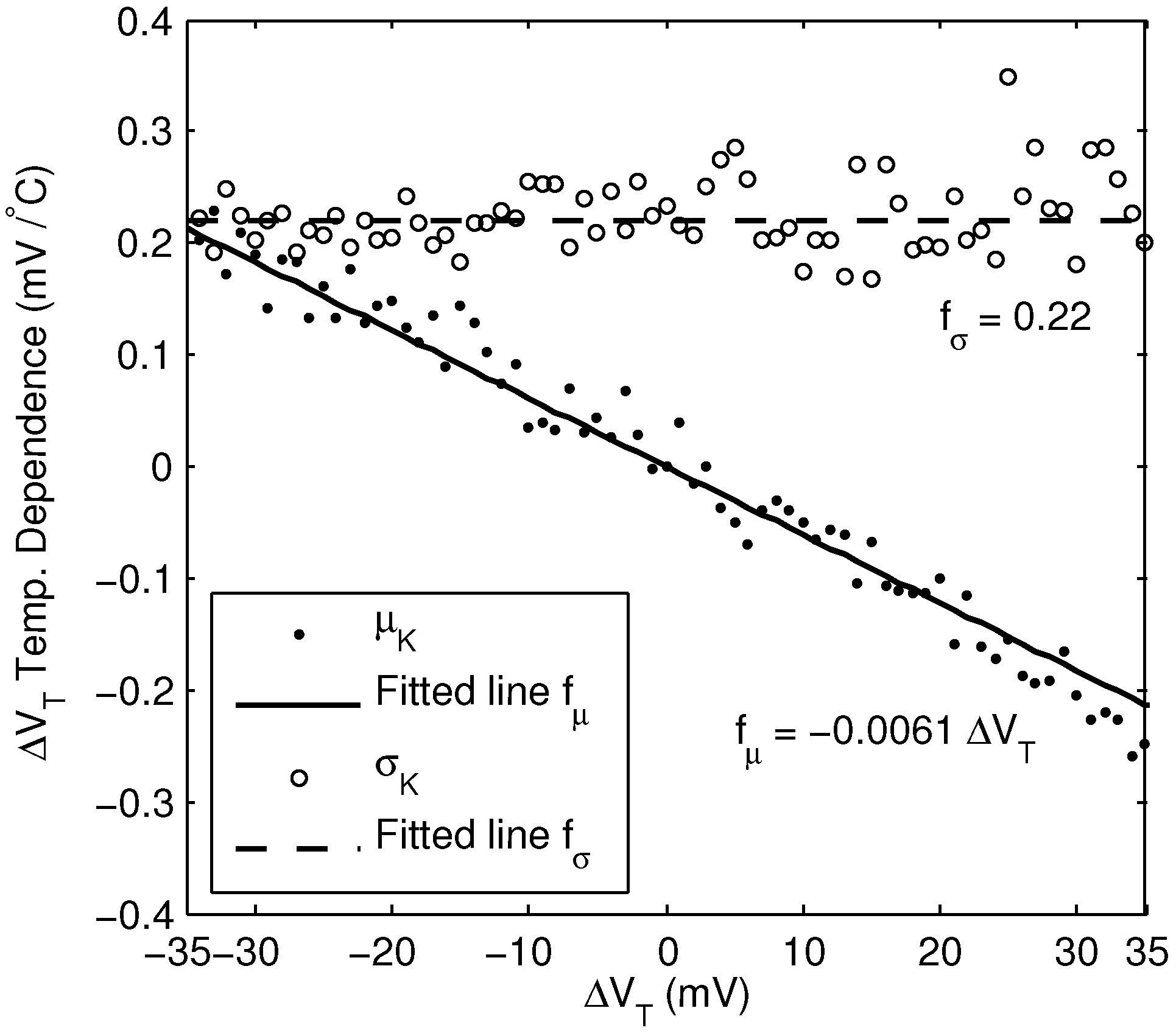
The temperature coefficient,
a, was found to be −6.1 × 10
C
. Because
a is negative, the magnitude of
tends to decrease as temperature increases. The standard deviation of
K was found to be
mV/
C. A plot of the mean and standard deviation of the temperature dependence is shown in
Figure 11, over a range of
values.
A possible explanation for the apparent randomness of the temperature dependence is that the devices M1 and M2 in
Figure 1 are assumed to differ only in their values of
, when in fact other device parameters such as the mobility
, gate oxide capacitance
, and effective dimensions
W and
L will vary as well [
19]. For example, in the preceding characterization scheme, if devices M1 and M2 are determined to have equal drain currents when driven with equal gate voltages, it is assumed that their values of
are equal. However, it could also be that their values of
are unequal, and other devices parameters are unequal in such a way that the drain currents remain equal. These other device parameters will then have their own, unequal temperature dependence [
20], resulting in the apparent random temperature dependence. A possible improvement to this work would be a more elaborate characterization scheme in which the mismatch between devices M1 and M2 could be more completely determined, although this would increase the complexity of the characterization scheme.
Figure 11.
Mean and standard deviation of the change in per 1 C change in temperature, derived from measurement of 15,360 bits of a single chip.
Figure 11.
Mean and standard deviation of the change in per 1 C change in temperature, derived from measurement of 15,360 bits of a single chip.
The practical effect of this is that a larger value of
must be selected for reliable operation, due to the combined effects of electronic noise and temperature dependence. For positive values of
, and if all temperature dependencies are assumed to fall within
, then the worst case temperature shift from
to
over an increase in temperature
is
Rearranging Equation (
23) and substituting
and
gives the value of
measured at nominal temperature that is required to ensure
after a temperature increase of
.
That is, by only selecting ID cells with
, it is ensured that after a
increase in temperature, the new threshold voltage difference will satisfy the original reliability requirement,
. For example, using the previously determined value of
mV, and assuming a possible temperature increase of 10
C, Equation (
24) indicates that
mV. This increases the fraction of unreliable bits to
.
This method could be employed by determining the parameters
a and
σ of Equation (
24) once for a particular manufacturing process. The characterization of individual chips would then not require any extra measurements beyond the two already required by the characterization scheme, and these measurements do not have to be taken at a particular temperature. This method is, however, inefficient due to the constraint imposed by Equation (
23), which assumes the worst case temperature dependence. This is highly unlikely for any given ID cell; a large fraction of cells characterized in this way as unreliable would in fact behave reliably. An obvious alternative would be simply to characterize each cell twice, once at each extreme of the expected operating temperature range, and only select cells that have the same classification at both extremes as reliable. This is more efficient, in the sense that the fraction of unreliable bits will be smaller, but requires a temperature controlled environment for characterizing each chip, which is frequently expensive and time-consuming to employ.
5.2. Addressing Parameter Selection
The selection of the particular parameters of the addressing scheme depends heavily on the particular application. In most cases, the specifications will require the selection of three minimum requirements: (1) address space size (S); (2) yield (Y); and (3) error rate (). After these requirements are specified, the other parameters of the masked addressing scheme can be determined. The parameters of a hypothetical system are determined here using experimentally derived data, to give an indication of the performance of this work.
Consider a system with the specifications
,
,
, and a possible
C. Given the requirement
and Equation (
15), the following constraint is imposed
Given this constraint, a lower limit for
N can be found using Equation (
20), with
and
. The smallest value that satisfies these conditions is
, setting
. Finally the total error rate can be found using Equation (
19) to be
.
