Sub-Threshold Standard Cell Sizing Methodology and Library Comparison
Abstract
:1. Introduction
2. Sub-Threshold Cell Sizing Methodology
2.1. Sub-Threshold Current Distribution Model

 is the mobility; C is the oxide capacitance;
  the sub-threshold slope factor; and U is the thermal voltage.
  is the gate to source voltage;
  is the drain to source voltage;
  is the threshold voltage, consists of zero biasing voltage, terminal voltages and device size effects [17]. From Equation (1), one can see that the current has an exponential relationship with the gate-to-source voltage and the threshold voltage of the transistor.
 as a Normal distribution and model the distribution of the transistor current using [18,19] as follows:

 stands for the mean value and
  stands for the standard deviation. In this model
  and
and  are regarded as technology parameters for a given W and L set. With the width and length tuning,
  and
and  also change accordingly due to RSCE. Therefore, depending on the range of W and L , different distributions of the
  are used in the sizing model.
2.2. Sub-Threshold Cell Balancing Method
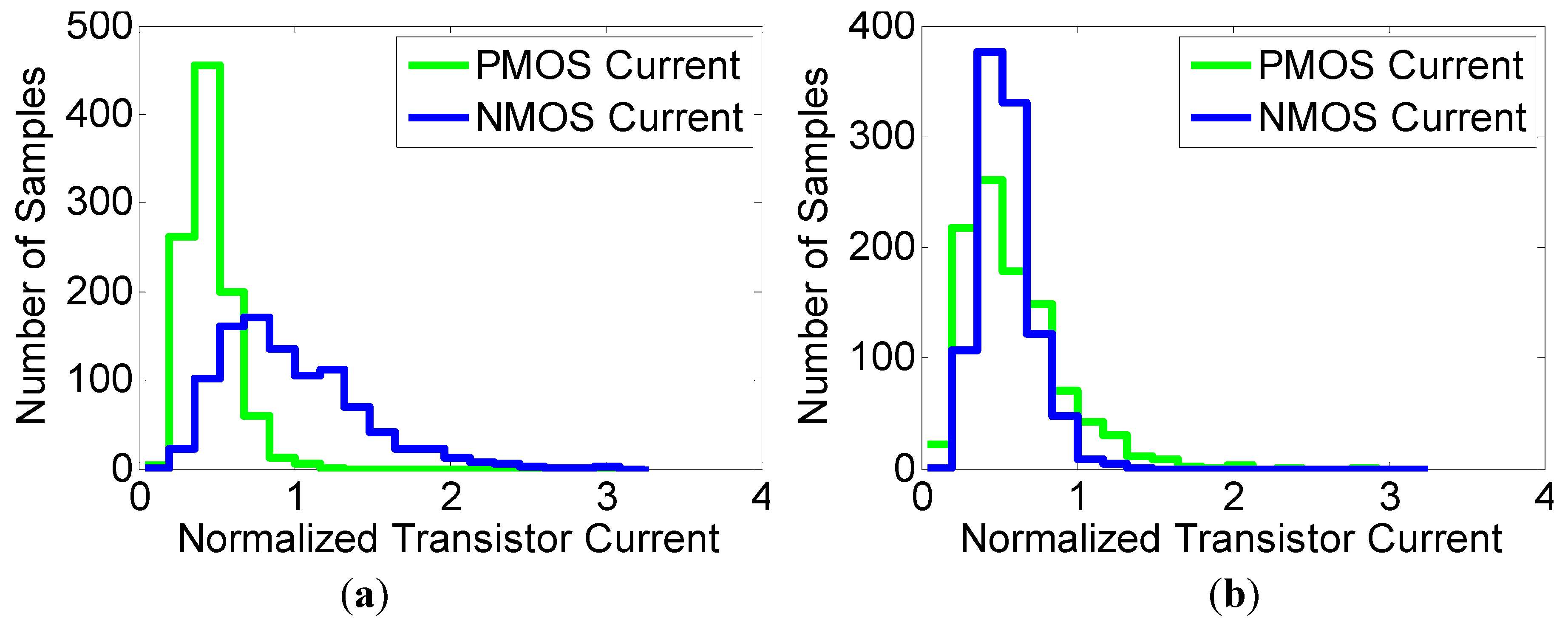
 . In the proposed sizing methodology, the ratio of the pull-up to pull-down transistors is determined by the balance between the current distributions of the PMOS and NMOS transistors. The difference with regard to the conventional sizing approach is that the current spread caused by the
  variation is taken into account.
 . From this, one can derive [1]:

 is a technology parameter defined by the mobility and oxide capacitance of the NMOS and PMOS transistors.
  is also used as the conventional sizing factor. Given the
  mean and variance values, Equation (3) serves as the current balancing equation. The NMOS and PMOS current distributions can be closely matched based on Equation (3).
2.3. Stack Sizing Model
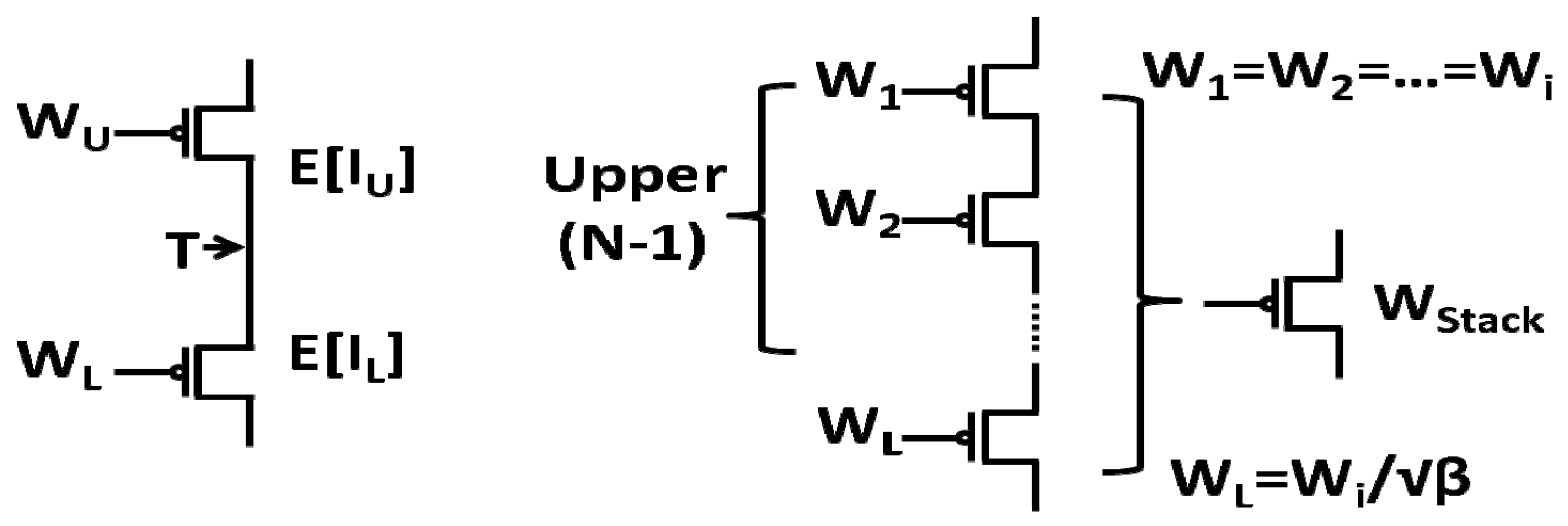
 PMOS transistors [lower
  NMOS transistors] have a similar impact on the current behavior of the stack. Therefore, let these
  transistors have equal sizes. Using the results of [9,20] to calculate the equivalent transistor width of the stack,
  , the mean current of
  transistors in a stack is calculated as follows [1]

 is a technology fitting parameter and λ is the DIBL effect coefficient [9]. To simplify the calculation of the equivalent transistor size of the stack, the length of each transistor in the stack is held fixed. Let the width of all
  transistors be
  and the width of the remaining transistor be
  , as shown in Figure 2. The width of the equivalent transistor is denoted as to
  . The same procedure holds for NMOS transistors.
 is also a technology dependent fitting parameter. With Equations (4) and (5), one can easily derive the optimal stack width ratio for the stack’s maximum current or minimum current spread. To achieve the maximum current, the lower PMOS (upper NMOS) transistor needs to be sized
  times smaller with regard to the upper PMOS (lower NMOS) transistors. The variation of the current stack can be written as:

 variation is treated as a given technology dependent parameter for given sizing (source bulk modulation is not taken into account). Table 1 is also an indicator of the large current variability when many transistors stacked transistors are used in the sub-threshold regime.
| Number of transistors in series | Simulation results | Normalized
 | Calculation from Equation (6) | |
|---|---|---|---|---|
 (A) (A) |  | |||
| 2 × 0.50 μm | 2.31 × 10⁻⁸ | 42.35% | 1 | 1 |
| 3 × 0.33 μm | 1.39 × 10⁻⁸ | 53.03% | 1.252 | 1.237 |
| 4 × 0.25 μm | 1.11 × 10⁻⁸ | 58.68% | 1.386 | 1.401 |
| 5 × 0.20 μm | 0.95 × 10⁻⁸ | 66.18% | 1.563 | 1.573 |
2.4. Parallel Sizing Model
 for
for  needs to be introduced to improve the accuracy of the model. This correlation factor was not needed in series-connected transistors because in that case the source-bulk modulation overshadows the correlation. The mean and variance of the current of N identical parallel connected transistors is [1]

 is the width of one single transistor,
  and
and  . The equivalent width for parallel transistors can be calculated from Equation (7) [1].

 times the width of the transistors in parallel.
 | Number of parallel transistors | Simulated  (A) (A) | Normalized  | Calculation from Equation (7) |
|---|---|---|---|
| 1 × 1.20 μm | 1.18 × 10⁻⁷ | 1.00 | 1.00 |
| 2 × 0.60 μm | 1.33 × 10⁻⁷ | 1.13 | 1.12 |
| 3 × 0.40 μm | 1.41 × 10⁻⁷ | 1.19 | 1.24 |
| 4 × 0.30 μm | 1.52 × 10⁻⁷ | 1.29 | 1.36 |
| 5 × 0.24 μm | 1.71 × 10⁻⁷ | 1.45 | 1.48 |
| 6 × 0.20 μm | 1.91 × 10⁻⁷ | 1.62 | 1.61 |
2.5. Complex Cell Translation
| Algorithm 1. |
| 1. If n transistors in Parallel |
| 2. Then Size of parallel transistors: |
| 3. W1 = W2 = … = Wn |
| 4. Parallel Equivalent Size: Equation (8) |
| 5. If m transistors in Series |
| 6. Then Size of transistors in stack: |
7.  |
| 8. Stack Equivalent Size: Equation (4) |
| 9. *U means next to output node; L means away from output node. |

 as the unit size of the N network. Then, the size of the equivalent transistor of B // C is
  according to Equation (8). With transistor A in series connection, the size of A can be defined by the second if then rule, as
  . The equivalent size of A, B // C is defined by Equation (4) as
  . The size of transistor D is equal to the size of the equivalent parallel-connected transistors. A similar procedure can be followed to size the transistors of the P network.
  for
for  and
and  for
for  . Then, the equivalent size of the worst-timing transition path in the N network becomes
  . This is balanced against the equivalent transistor resulting from the best timing transition path in the P network using Equation (3) to find the actual width values of
  for the N and P networks. Other combinations of equivalent transistors on the best/worst timing transition path of the N/P network can be derived accordingly.
3. Library Characterization
4. Library Comparisons

5. Circuit Synthesis Comparisons
5.1. ITC B14 Benchmark
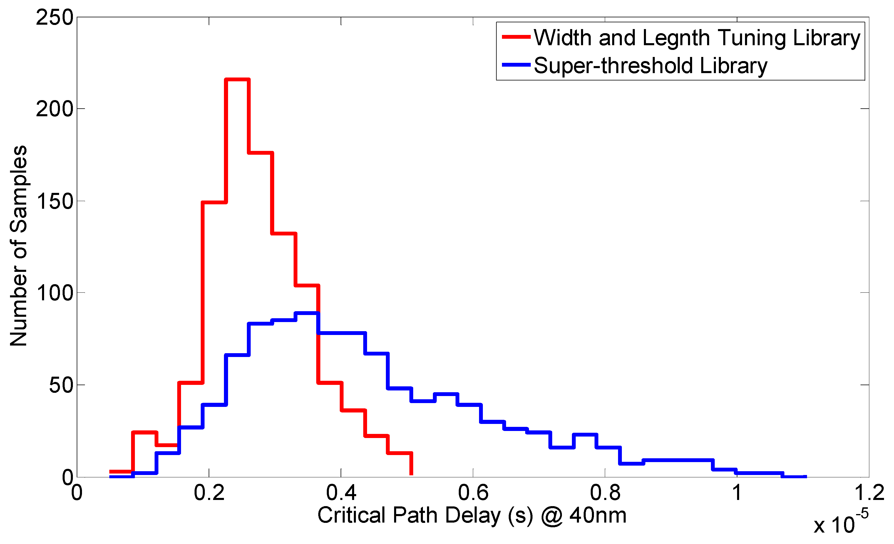
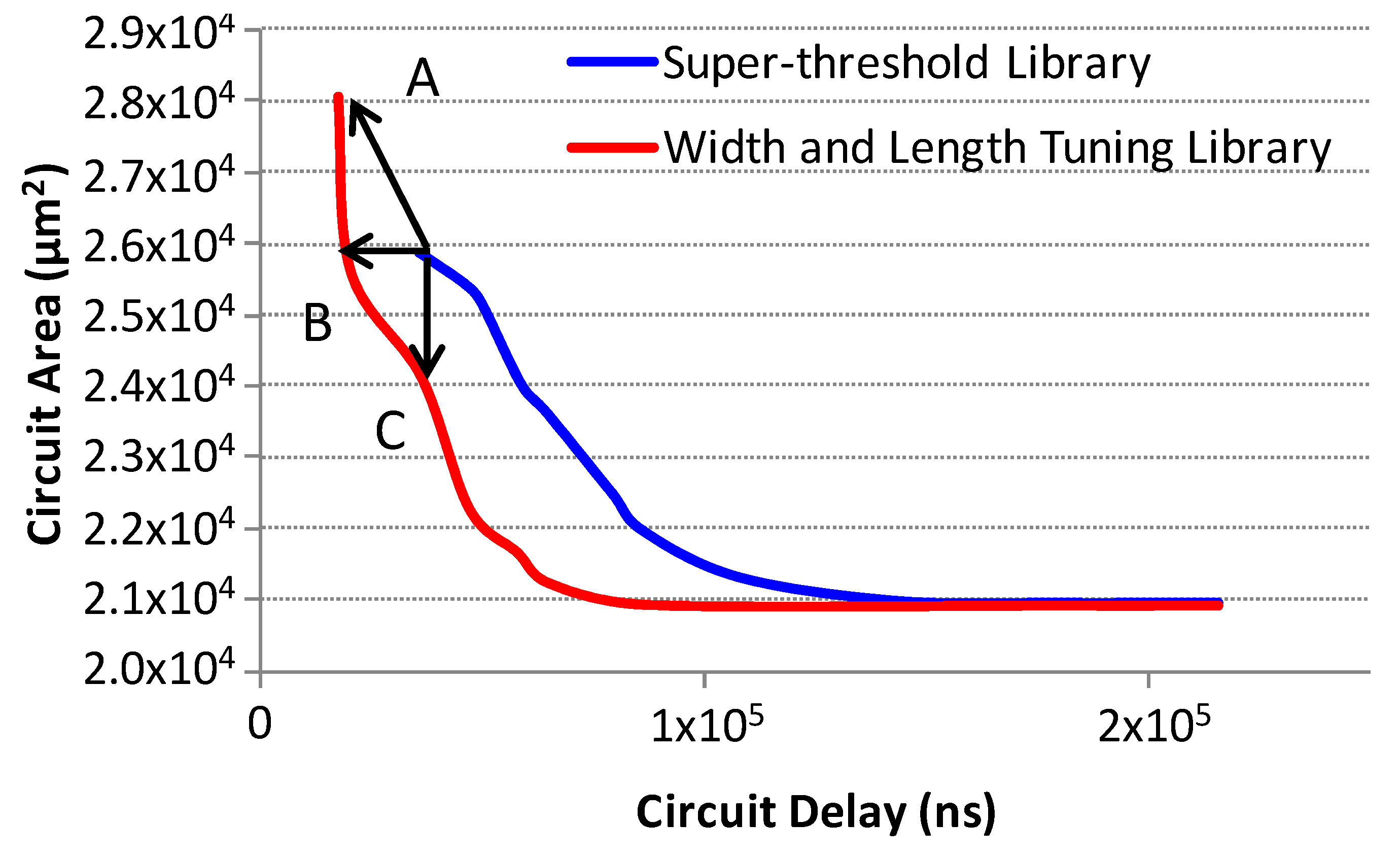
5.2. ITC Benchmark Circuits
| Delay (ns) | % | Area (μm2) | % | Total Power (nW) | % | ||||
|---|---|---|---|---|---|---|---|---|---|
| Super-threshold library | Width and length tuning | Super-threshold library | Width and length tuning | Super-threshold library | Width and length tuning | ||||
| B01 | 850 | 480 | 43.5 | 320 | 334 | −4.4 | 0.502 | 0.308 | 38.6 |
| B02 | 780 | 450 | 42.3 | 213 | 227 | −6.6 | 0.237 | 0.161 | 32.1 |
| B03 | 880 | 510 | 42.0 | 582 | 660 | −13.4 | 0.229 | 0.164 | 28.4 |
| B04 | 1170 | 630 | 46.2 | 2120 | 2525 | −19.1 | 1.267 | 0.865 | 31.7 |
| B05 | 1820 | 1030 | 43.4 | 3118 | 3664 | −17.5 | 1.336 | 0.920 | 31.1 |
| B14 | 3600 | 1720 | 52.2 | 25866 | 28056 | −8.5 | 3.795 | 2.780 | 26.7 |
| Delay (ns) | % | Area (μm2) | Total Power (nW) | % | ||||
|---|---|---|---|---|---|---|---|---|
| Super-threshold library | Width and length tuning | Super-threshold library | Width and length tuning | Super-threshold library | Width and length tuning | |||
| B01 | 850 | 500 | 41.2 | 320 | 315 | 0.502 | 0.298 | 40.6 |
| B02 | 780 | 490 | 37.2 | 213 | 204 | 0.237 | 0.148 | 37.6 |
| B03 | 880 | 750 | 14.8 | 582 | 555 | 0.229 | 0.138 | 39.7 |
| B04 | 1170 | 810 | 30.8 | 2120 | 2077 | 1.267 | 0.765 | 39.6 |
| B05 | 1820 | 1200 | 34.1 | 3118 | 3114 | 1.336 | 0.826 | 38.2 |
| B14 | 3600 | 2000 | 44.4 | 25866 | 25614 | 3.795 | 2.466 | 35.0 |
| Delay (ns) | Area (μm2) | % | Total Power (nW) | % | ||||
|---|---|---|---|---|---|---|---|---|
| Super-threshold library | Width and length tuning | Super-threshold library | Width and length tuning | Super-threshold library | Width and length tuning | |||
| B01 | 850 | 850 | 320 | 243 | 24.1 | 0.502 | 0.238 | 52.6 |
| B02 | 780 | 780 | 213 | 177 | 16.9 | 0.237 | 0.144 | 39.2 |
| B03 | 880 | 880 | 582 | 536 | 7.9 | 0.229 | 0.139 | 39.3 |
| B04 | 1170 | 1170 | 2120 | 1671 | 21.2 | 1.267 | 0.877 | 30.8 |
| B05 | 1820 | 1820 | 3118 | 2726 | 12.6 | 1.336 | 0.723 | 45.9 |
| B14 | 3600 | 3600 | 25866 | 24121 | 6.7 | 3.795 | 2.852 | 24.8 |
6. Conclusions
References
- Liu, B.; Ashouei, M.; Huisken, J.; de Gyvez, J.P. Standard Cell Sizing for Subthreshold Operation. In Proceedings of the 49th Design Automation Conference (DAC), San Fransico, CA, USA, 3–7 June 2012; pp. 962–967.
- Liu, B.; de Gyvez, J.P.; Ashouei, M. Library Tuning for Subthreshold Operation. In Proceedings of the 2012 IEEE Subthreshold Microelectronics Conference (SubVT), Waltham, MA, USA, 9–10 October 2012; pp. 1–3.
- Calhoun, B.H.; Wang, A.; Chandrakasan, A. Modeling and sizing for minimum energy operation in subthreshold circuits. Solid-State Circ. IEEE J. 2005, 40, 1778–1786. [Google Scholar]
- Kwong, J.; Ramadass, Y.; Verma, N.; Koesler, M.; Huber, K.; Moormann, H.; Chandrakasan, A. A 65nm Sub-Vt Microcontroller with Integrated SRAM and Switched-Capacitor DC-DC Converter. In Proceedings of the IEEE International Solid-State Circuits Conference (ISSCC), San Fransico, CA, USA, 3–7 February 2008; pp. 318–616.
- Seok, M.; Jeon, D.; Chakrabarti, C.; Blaauw, D.; Sylvester, D. A 0.27V 30MHz 17.7nJ/Transform 1024-pt Complex FFT Core with Super-Pipelining. In Proceedings of the 2011 IEEE International Solid-State Circuits Conference Digest of Technical Papers (ISSCC), San Fransico, CA, USA, 20–24 February 2011; pp. 342–344.
- Bol, D.; Kamel, D.; Flandre, D.; Legat, J.-D. Nanometer MOSFET Effects on the Minimum-Energy Point of 45nm Subthreshold Logic. In Proceedings of the 14th ACM/IEEE International Symposium on Low Power Electronics and Design, San Fancisco, CA, USA, 19–21 August 2009; pp. 3–8.
- Kwong, J.; Chandrakasan, A.P. Variation-Driven Device Sizing for Minimum Energy Sub-Threshold Circuits. In Proceedings of the 2006 International Symposium on Low Power Electronics and Design (ISLPED), Tegernsee Germany, 4–6 October 2006; pp. 8–13.
- Kim, T.-H.; Hanyong, E.; Keane, J.; Kim, C. Utilizing Reverse Short Channel Effect for Optimal Subthreshold Circuit Design. In Proceedings of the 2006 International Symposium on Low Power Electronics and Design (ISLPED), Tegernsee, Germany, 4–6 October 2006; pp. 127–130.
- Keane, J.; Hanyong, E.; Tae-Hyoung, K.; Sapatnekar, S.; Kim, C. Subthreshold Logical Effort: A Systematic Framework for Optimal Subthreshold Device Sizing. In Proceedings of the 43rd Design Automation Conference, San Fransico, CA, USA, 24–24 June 2006; pp. 425–428.
- Jun, Z.; Jayapal, S.; Busze, B.; Huang, L.; Stuyt, J. A 40 nm Inverse-Narrow-Width-Effect-Aware Sub-Threshold Standard Cell Library. In Proceedings of the 48th Design Automation Conference (DAC), San Diego, CA, USA, 5–9 June 2011; pp. 441–446.
- Bol, D.; Flandre, D.; Legat, J.-D. Technology Flavor Selection and Adaptive Techniques for Timing-constrained 45nm Subthreshold Circuits. In Proceedings of the 14th International Symposium on Low Power Electronics and Design, San Fancisco, CA, USA, 19–21 August, 2009; pp. 21–26.
- Bol, D.; de Vos, J.; Hocquet, C.; Botman, F.; Durvaux, F.; Boyd, S.; Flandre, D.; Legat, J. SleepWalker: A 25-MHz 0.4-V Sub-mm2 7-uW/MHzMicrocontroller in 65-nm LP/GP CMOS for low-carbon wireless sensor nodes. Solid-State Circ. IEEE J. 2013, 48, 20–32. [Google Scholar]
- Blesken, M.; Lu, X; Tkemeier, S.; Ruckert, U. Multiobjective Optimization for Transistor Sizing Sub-threshold CMOS Logic Standard Cells. In Proceedings of 2010 IEEE International Symposium on Circuits and Systems, Paris, France, 30 May–2 June 2010; pp. 1480–1483.
- Abouzeid, F.; Clerc, S.; Firmin, F.; Renaudin, M.; Sicard, G. A 45nm CMOS 0.35v-optimized Standard Cell Library for Ultra-low power Applications. In Proceedings of the 14th ACM/IEEE International Symposium on Low Power Electronics and Design, San Fancisco, CA, USA, 19–21 August 2009; pp. 225–230.
- Tsividis, Y. Operation and Modeling of the Mos Transistor (The Oxford Series in Electrical and Computer Engineering); Oxford University Press: New York, USA, 2004; pp. 62–96. [Google Scholar]
- Wang, A.; Calhoun, B.H.; Chandrakasan, A.P. Sub-Threshold Design for Ultra Low-Power Systems; Springer: New York, USA, 2006; pp. 27–32. [Google Scholar]
- Avant, Star-Hspice User's Manual; Synopsys: Mountain View, CA, USA, 2000; pp. 798–801.
- Crow, E.L.; Shimizu, K. Lognormal Distributions: Theory and Applications; Marcel Dekker: New York, NY, USA, 1988; pp. 195–210. [Google Scholar]
- Bo, Z.; Hanson, S.; Blaauw, D.; Sylvester, D. Analysis and Mitigation of Variability in Subthreshold Design. In Proceedings of the 2005 International Symposium on Low Power Electronics and Design, San Diego, CA, USA, 8–10 August 2005; pp. 20–25.
- Al-Hertani, H.; Al-Khalili, D.; Rozon, C. A New Subthreshold Leakage Model for NMOS transistor Stacks. In Proceedings of the IEEE Northeast Workshop on Circuits and Systems, Montreal, Canada, 5–8 August 2007; pp. 972–975.
- Fenton, L. The sum of log-normal probability distributions in scatter transmission systems. Commun. Syst. IRE Trans. 1960, 8, 57–67. [Google Scholar]
- Gemmeke, T.; Ashouei, M. Variability Aware Cell Library Optimization for Reliable Sub-Threshold Operation. In Proceedings of the European Solid States Circuits Conference (ESSCIRC), Bordeaux, France, 17–21 September 2012; pp. 42–45.
- Bhasker, J.; Chadha, R. Static Timing Analysis for Nanometer Designs: A Practical Approach; Springer: New York, USA, 2009; pp. 26–43. [Google Scholar]
- Pelgrom, M.J.M.; Duinmaijer, A.C.J.; Welbers, A.P.G. Matching properties of MOS transistors. Solid-State Circ. IEEE J. 1989, 24, 1433–1439. [Google Scholar]
- Corno, F.; Reorda, M.S.; Squillero, G. RT-level ITC'99 benchmarks and first ATPG results. Des. Test Comput. IEEE 2000, 17, 44–53. [Google Scholar] [CrossRef]
© 2013 by the authors; licensee MDPI, Basel, Switzerland. This article is an open access article distributed under the terms and conditions of the Creative Commons Attribution license (http://creativecommons.org/licenses/by/3.0/).
Share and Cite
Liu, B.; De Gyvez, J.P.; Ashouei, M. Sub-Threshold Standard Cell Sizing Methodology and Library Comparison. J. Low Power Electron. Appl. 2013, 3, 233-249. https://doi.org/10.3390/jlpea3030233
Liu B, De Gyvez JP, Ashouei M. Sub-Threshold Standard Cell Sizing Methodology and Library Comparison. Journal of Low Power Electronics and Applications. 2013; 3(3):233-249. https://doi.org/10.3390/jlpea3030233
Chicago/Turabian StyleLiu, Bo, Jose Pineda De Gyvez, and Maryam Ashouei. 2013. "Sub-Threshold Standard Cell Sizing Methodology and Library Comparison" Journal of Low Power Electronics and Applications 3, no. 3: 233-249. https://doi.org/10.3390/jlpea3030233
APA StyleLiu, B., De Gyvez, J. P., & Ashouei, M. (2013). Sub-Threshold Standard Cell Sizing Methodology and Library Comparison. Journal of Low Power Electronics and Applications, 3(3), 233-249. https://doi.org/10.3390/jlpea3030233


