A Digital Auto-Zeroing Circuit to Reduce Offset in Sub-Threshold Sense Amplifiers

Abstract
:1. Introduction
 that is achieved for strong inversion operation. In addition it causes increased cell instability and a severely degraded read-current [1,2]. Several attempts have been made before to tackle the problem of offset voltage in sense amplifiers (SAs) including redundancy [3], transistor upsizing [4], digitally controlled compensation [5] and dynamic compensation [6]. Our approach to eliminating offset is a digital auto-zeroing (DAZ) scheme inspired by analog amplifier offset correction [7]. The main advantages of the approach are the near-zero offset after cancellation, offset tuning, and the automatic temperature, voltage, and aging tracking achievable using a repeated offset calibration phase, which makes the design useful in the sub-threshold region due to the high offset voltage sensitivity to supply voltage and temperature variations. In Verma and Chandrakasan [3], SA redundancy is used. It requires the SRAM bit-line from each column be connected to N different SAs. One SA will be selected whose offset is bound by the high and low logic levels of bit-line. This scheme statistically reduces the reliance on SAs with high offset, but it adds area and test time calibration to select the SA to use from each set. In Pileggi [4], transistor upsizing is used. A linear response surface model was developed to relate the SA offset voltage to the threshold voltages variations. The model is used to determine the statistical optimized transistors sizing. The optimized design resulted in a 25% decrease in the standard deviation of the offset voltage at a cost of 10% increase in active area. In Ryan and Calhoun [1], a methodology is proposed for sizing sub-VT SAs to minimize offset using SAs for ultra-low power operation. In Bhargava [5] a digitally controlled compensation is used. The scheme is applied to a latch-style and Strong-ARM SA topologies. Measured results from a 45nm test-chip show that the standard deviation of the offset is reduced by 5X. In Sachdev [6], dynamic compensation is used. A group of transistors are selectively coupled to high and low voltage levels via multi-phase timing. This results in a voltage level on nodes of interest that is a function of transistor mismatch. The voltage levels act to compensate for the transistor mismatch. This scheme is similar to the auto-zeroing scheme presented in this work. However the presented scheme uses a compensation capacitor, charge pump and feed-back circuit. Hence, the calibration phase is not necessarily needed prior to every sensing cycle. This improves the SA power consumption as will be illustrated in Section 5.
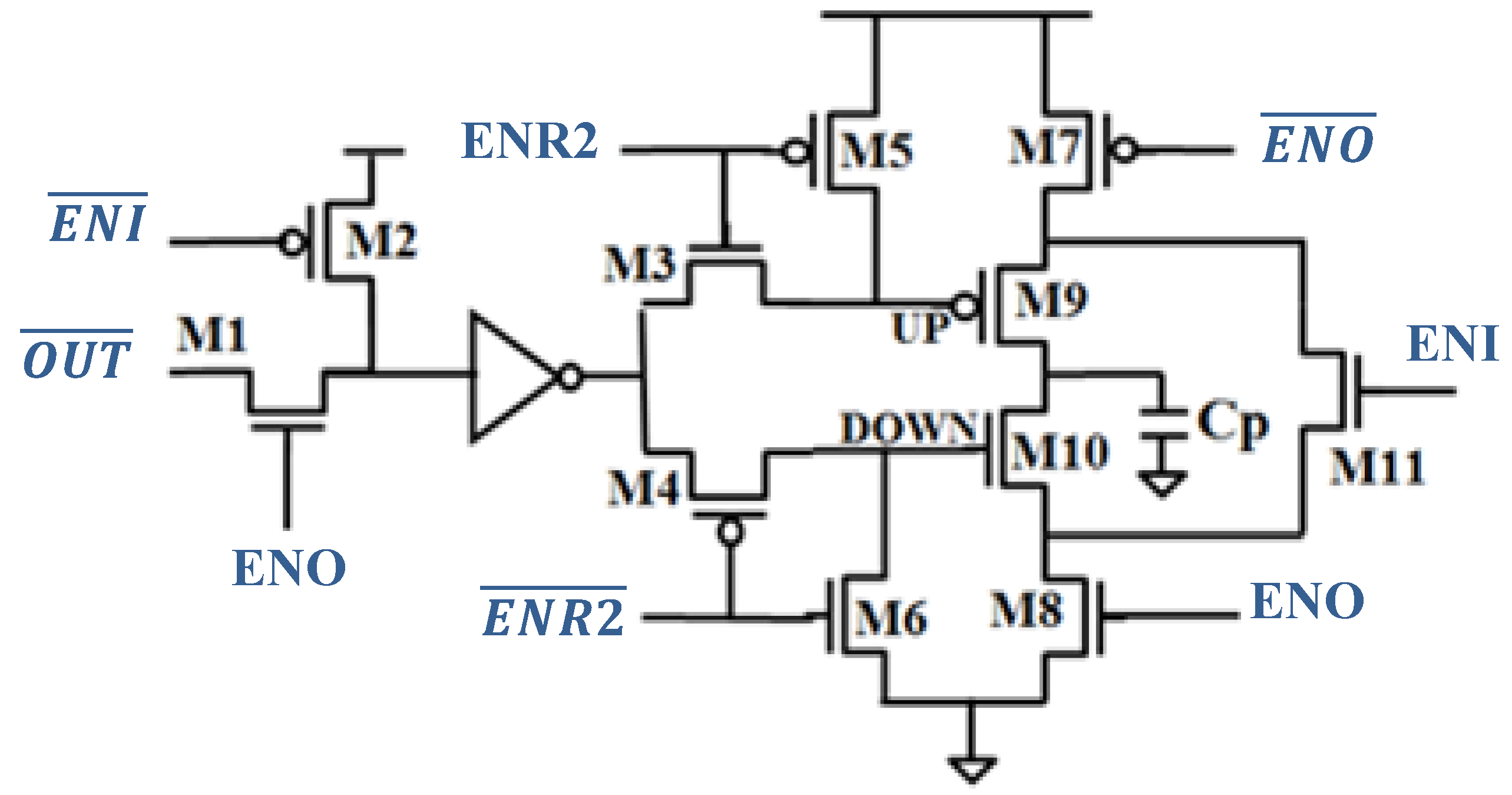
2. Mismatch Compensation using Auto- Zeroing Circuitry

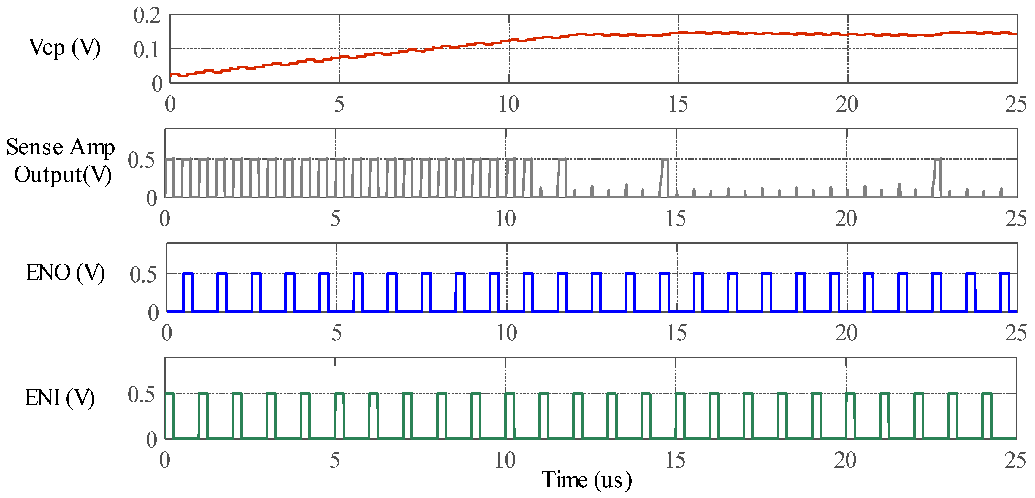

3. Voltage, Temperature, and Aging Tracking
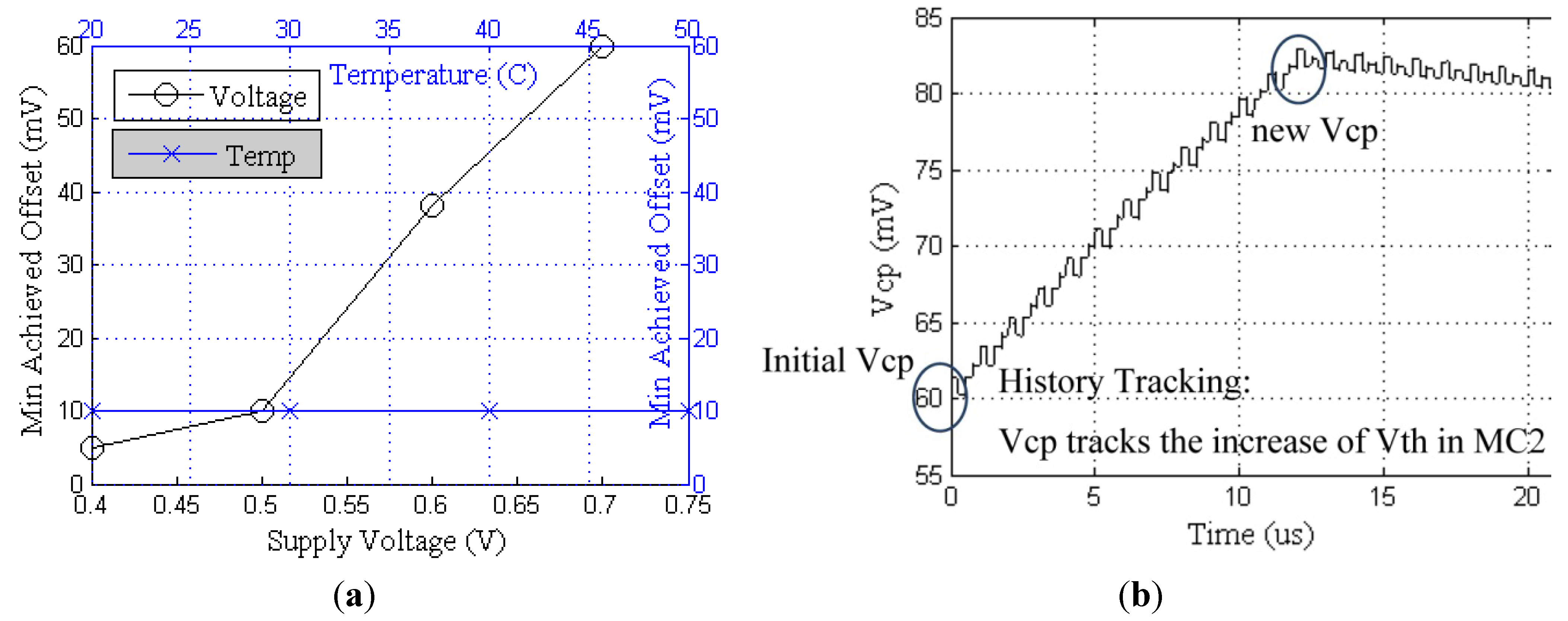
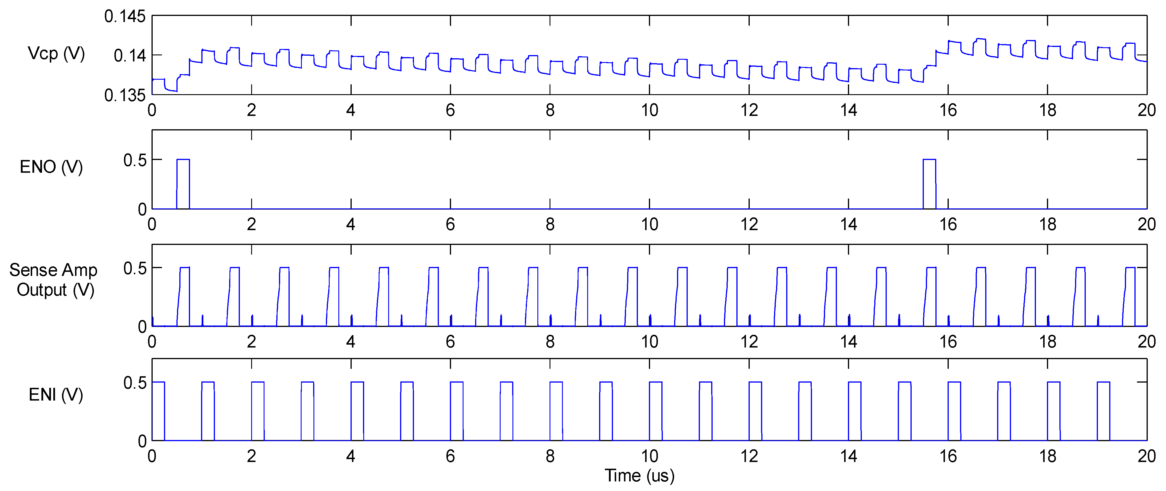
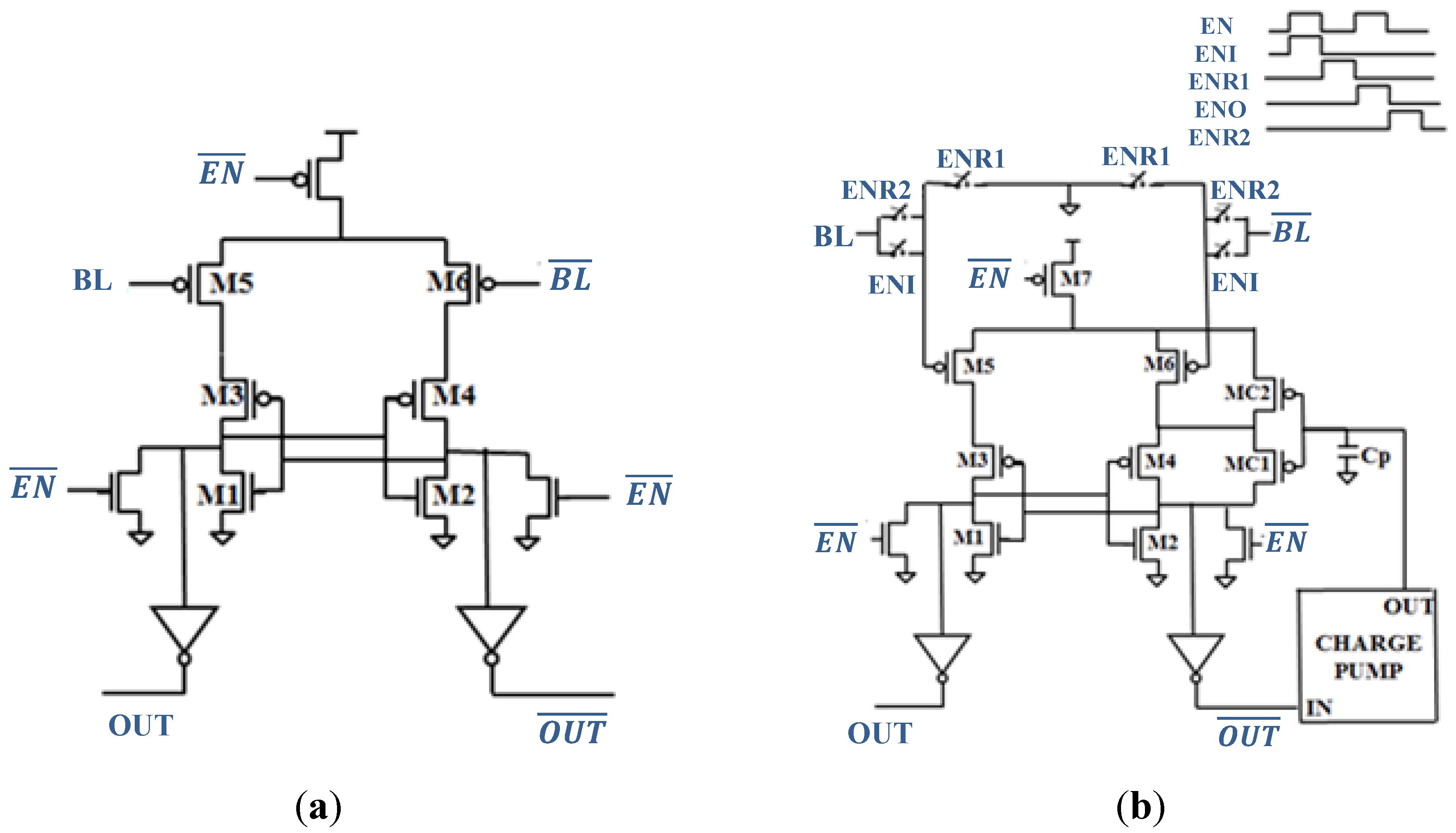
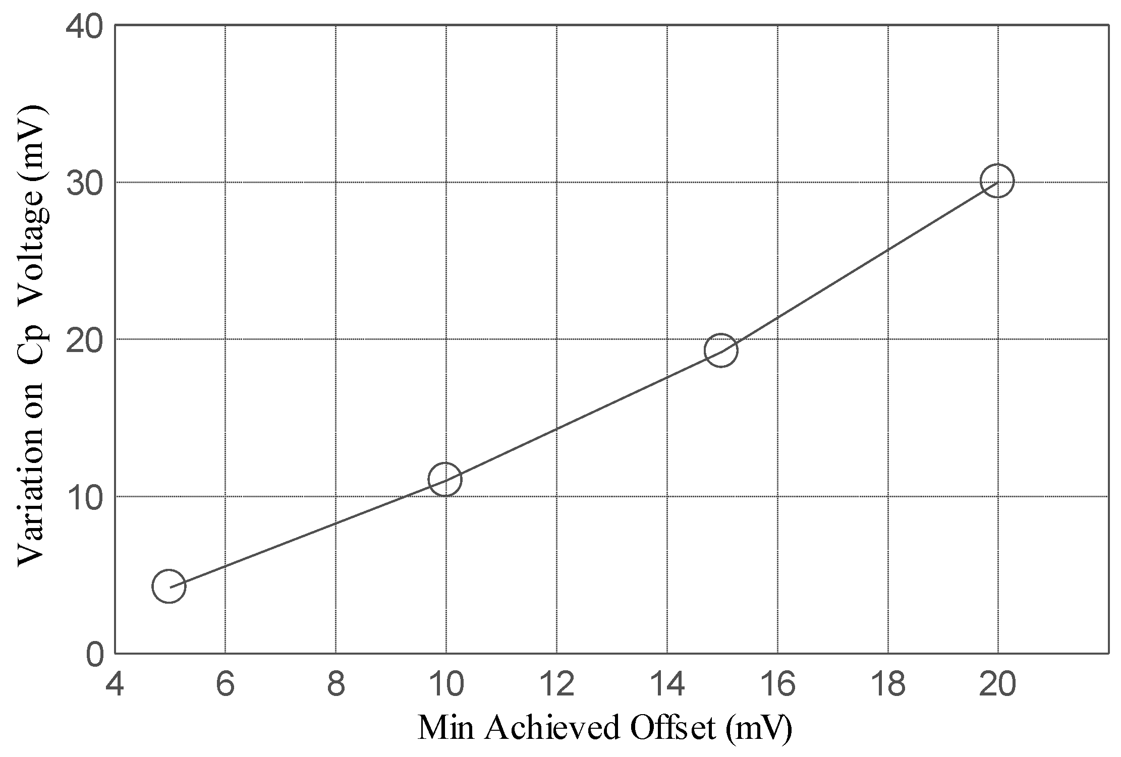
4. Offset Tuning

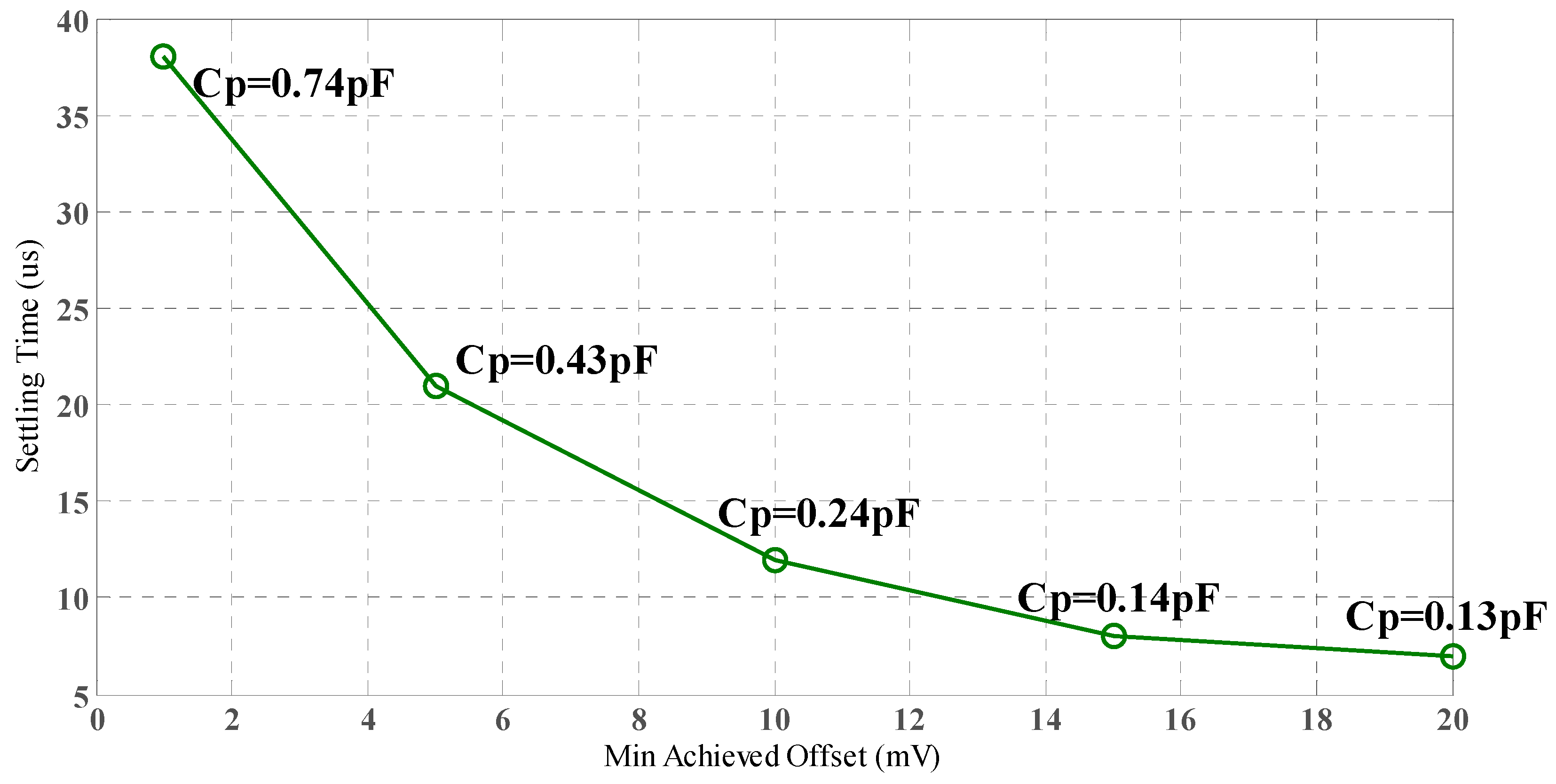
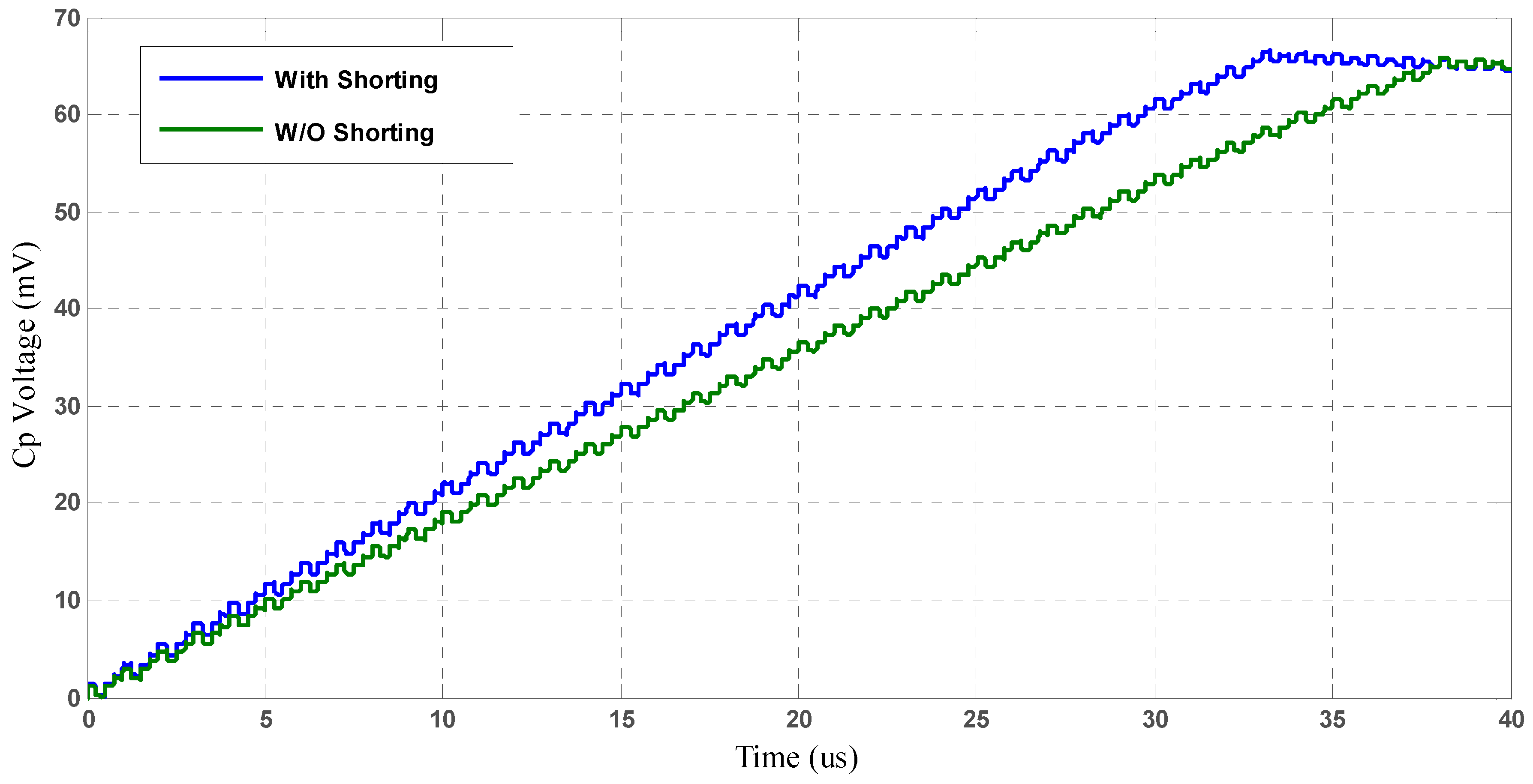
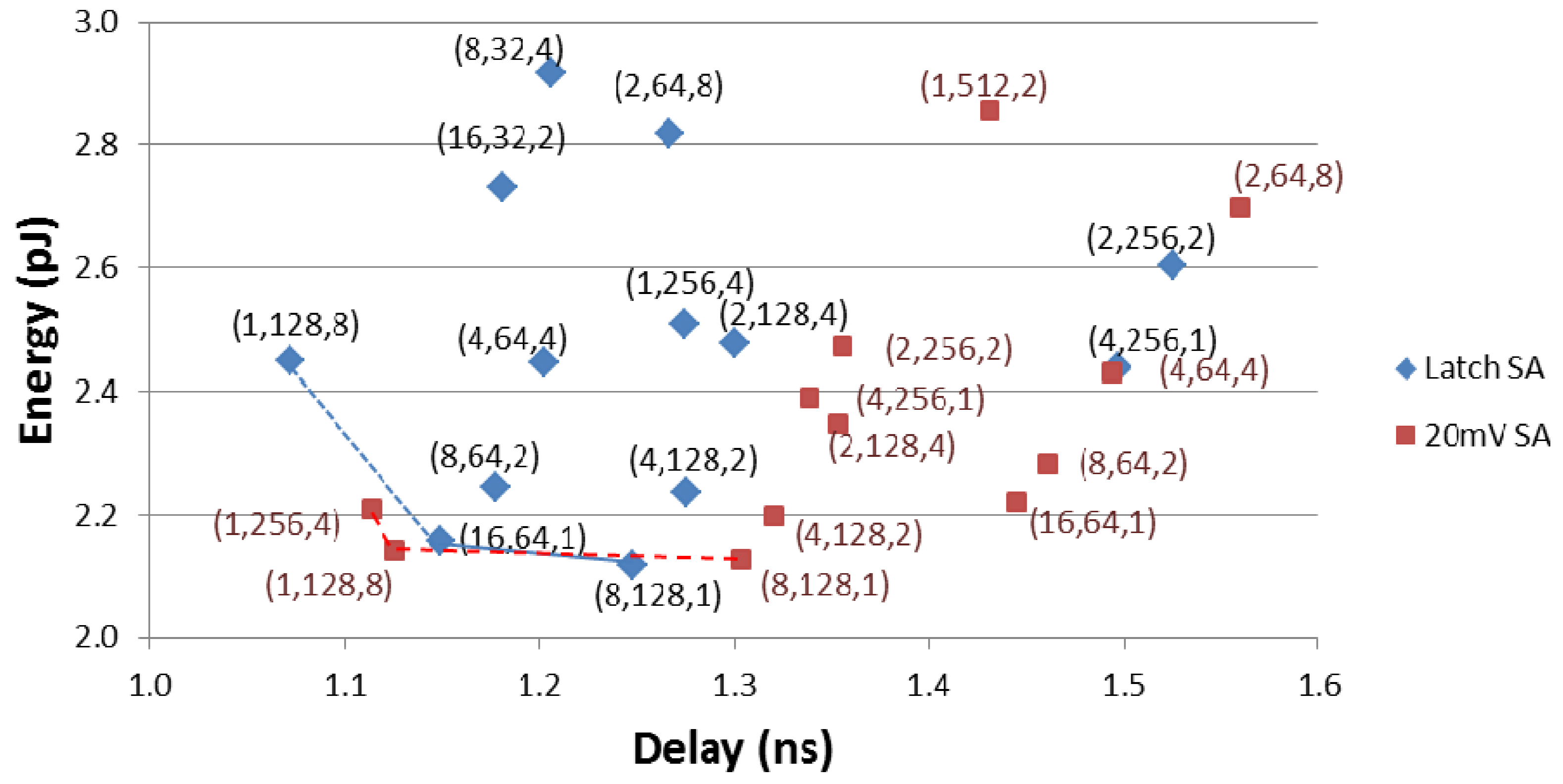
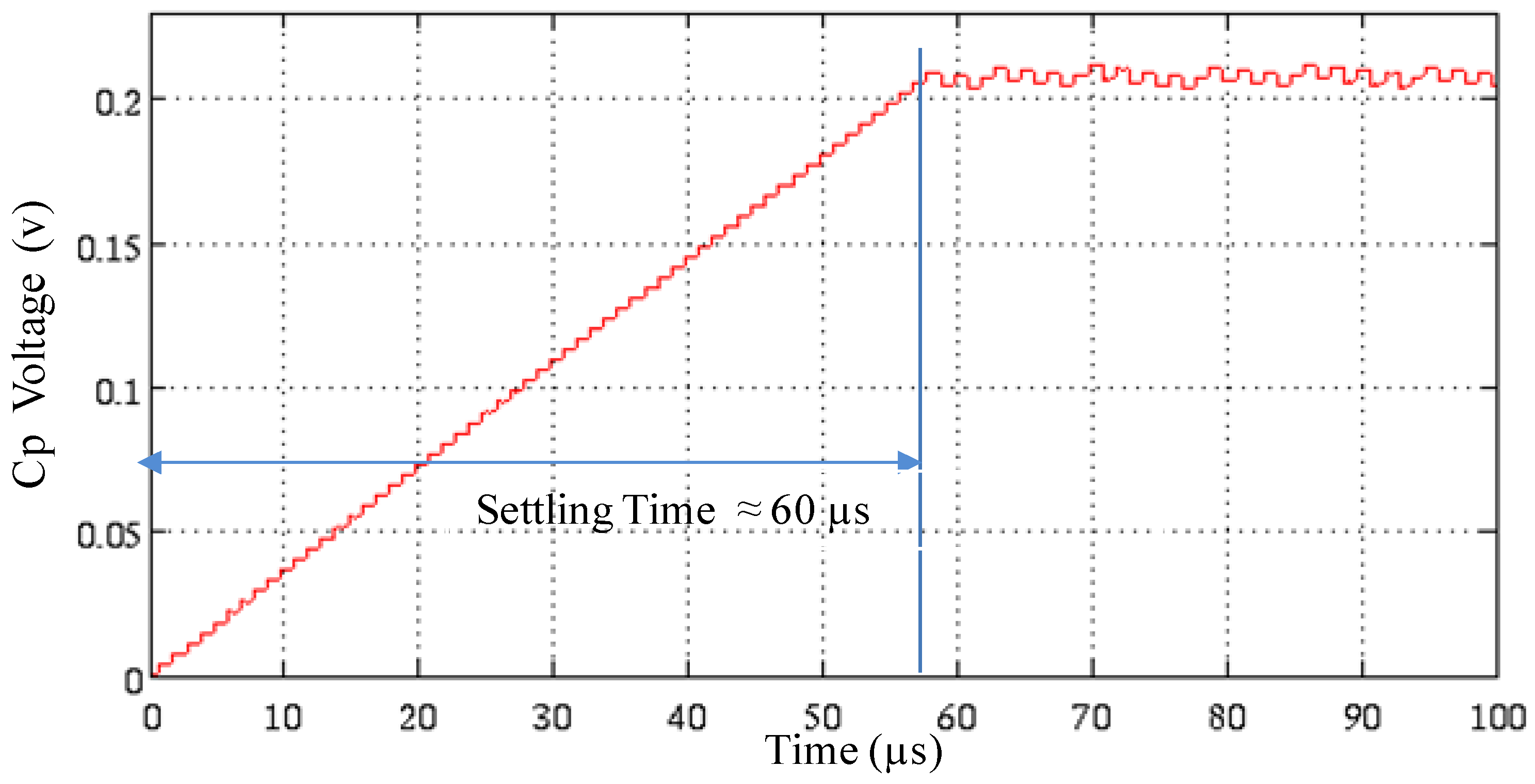
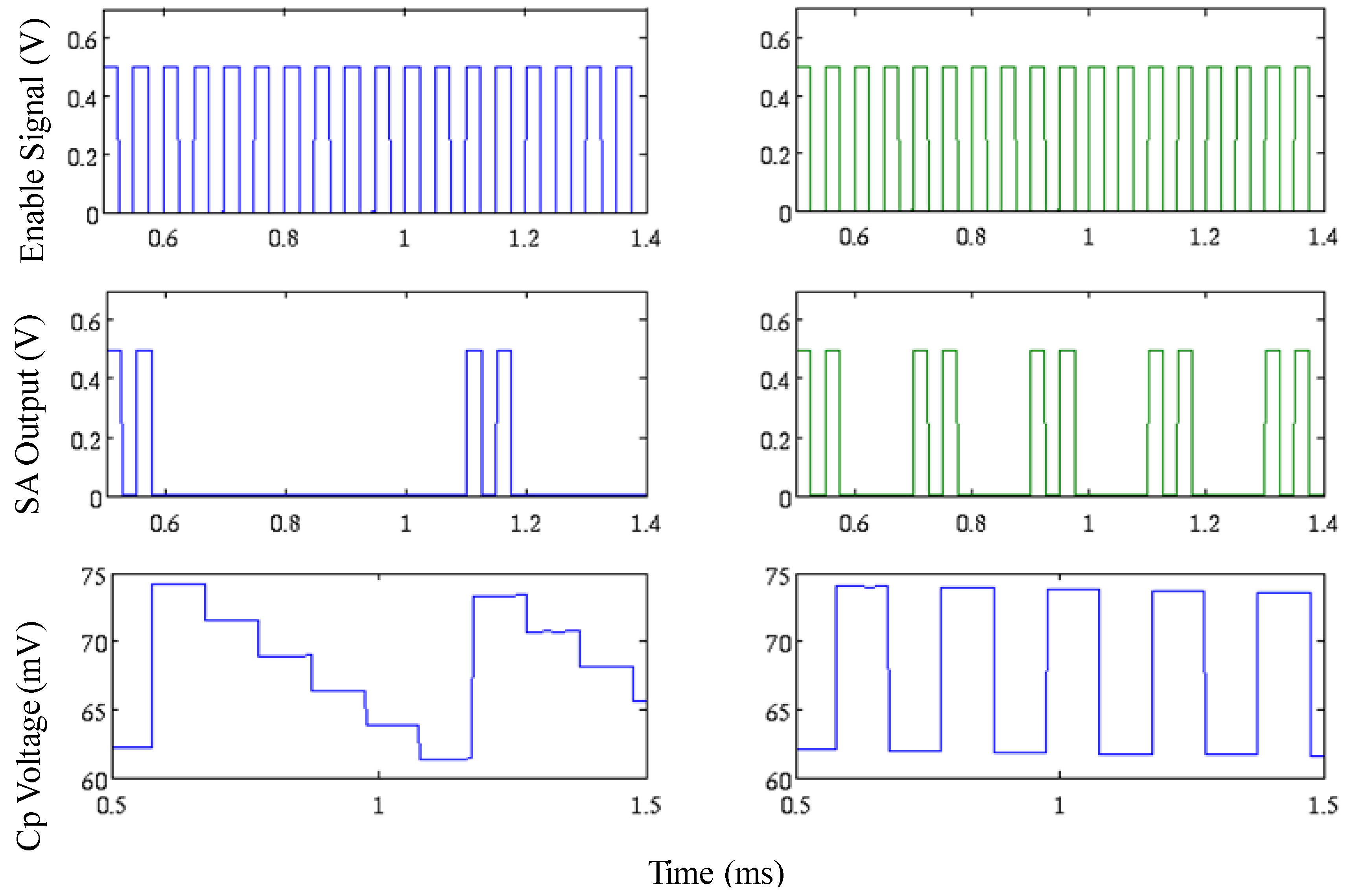
5. Power Consumption

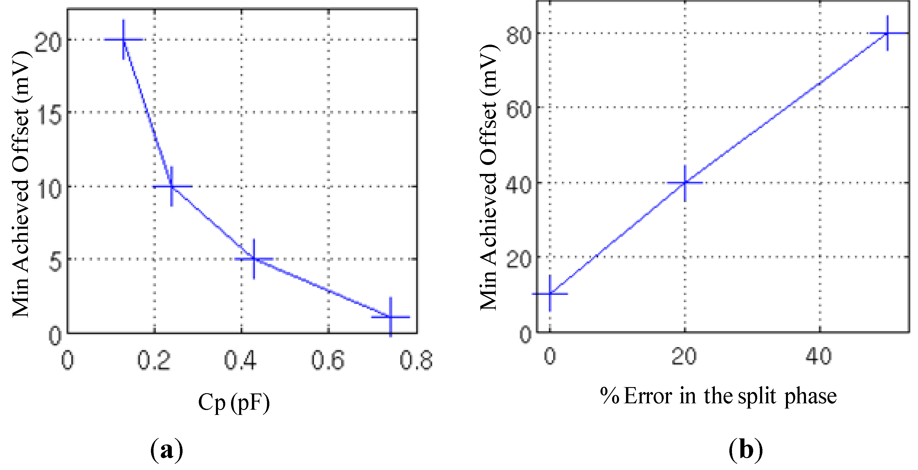
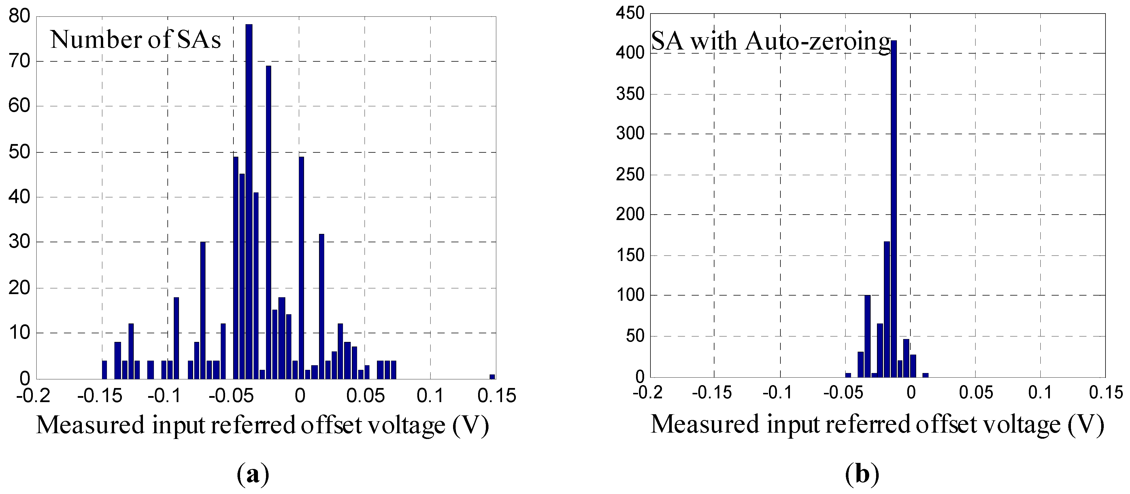
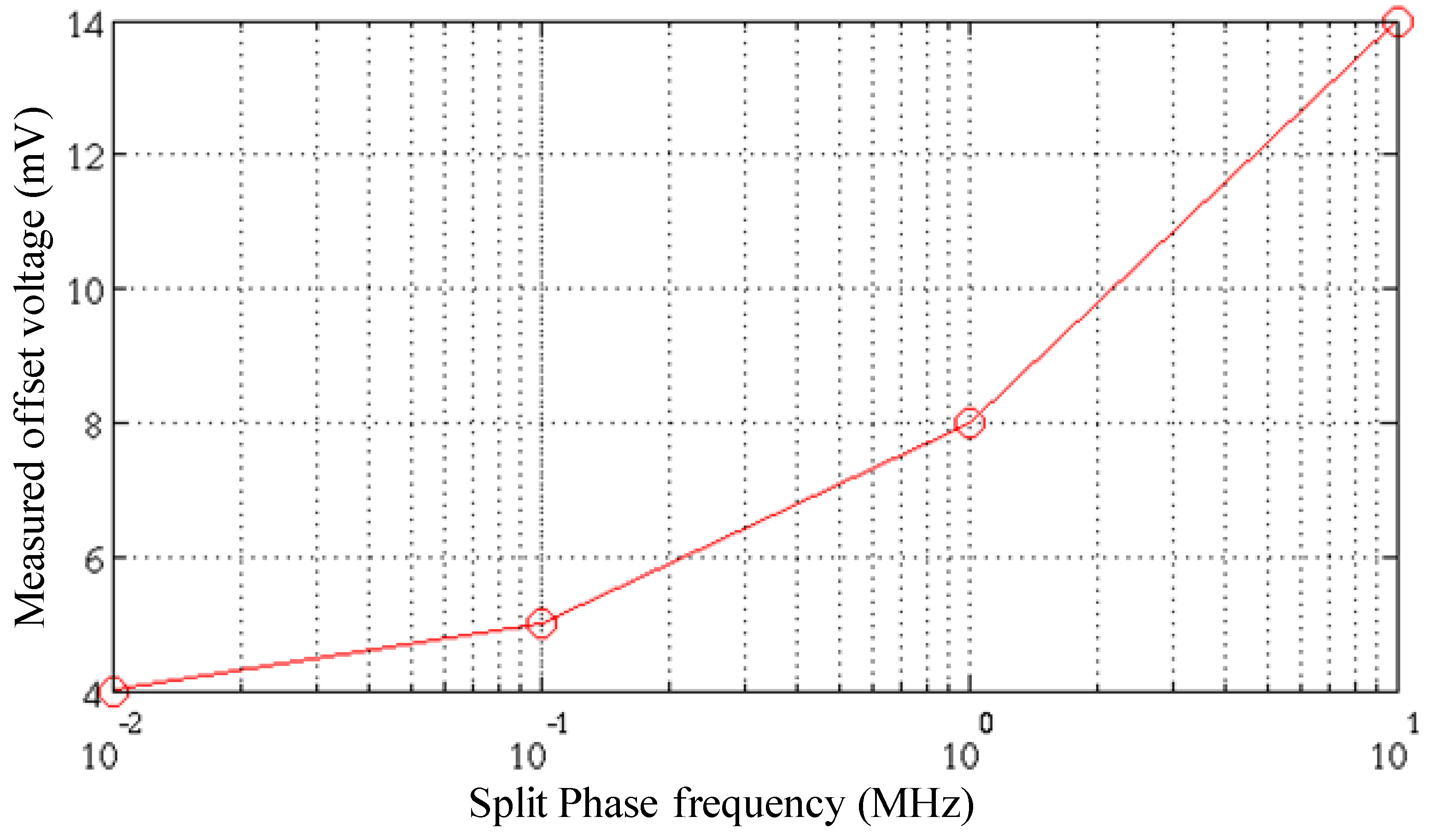
6. Offset Sensitivity
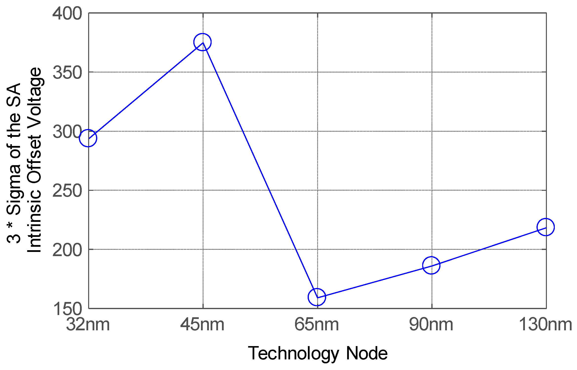
7. Offset Compensation across Technology Nodes
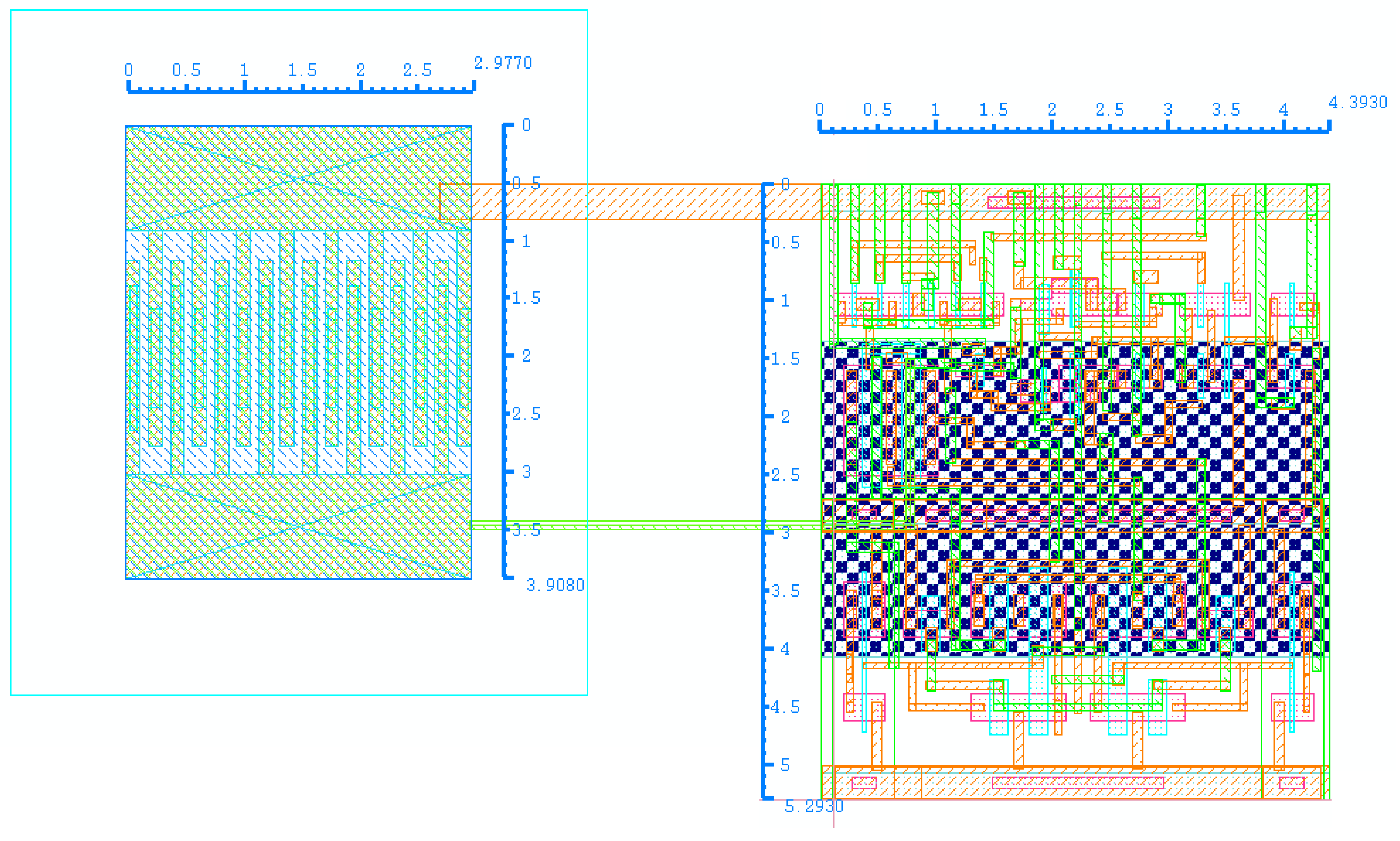
8. 16 kB SRAM Design
9. Comparison to other Offset Compensation Schemes

| Offset Compensation Scheme | Power Consumption | Settling time |
|---|---|---|
| DAZ SA | 6 nW | 12 μs |
| Dynamic Compensation [6] | 4 nW | 0.5 μs |
| DAZ SA with controllable offset phase | 2.5 nW | 12 μs |
10. 45 nm Test Chip Measurements


11. Conclusions
References
- Ryan, J.F.; Calhoun, B.H. Minimizing Offset for Latching Voltage-Mode Sense Amplifiers for Sub-Threshold Operation. In Proceedings of the 9th International Symposium on Quality Electronic Design, San Jose, California, USA, 17–19 March 2008; pp. 127–132.
- Wang, A.; Chandrakasan, A.P.; Kosonocky, S.V. Optimal Supply and Threshold Scaling for Subthreshold CMOS Circuits. In Proceedings of the IEEE Computer Society Annual Symposium on VLSI, Pittsburgh, PA, USA, 25–26 April 2002; pp. 5–9.
- Verma, N.; Chandrakasan, A.P. A 256 kb 65 nm 8T subthreshold SRAM employing sense-amplifier redundancy. IEEE J. Solid State Circ. 2008, 43, 141–149. [Google Scholar] [CrossRef]
- Pileggi, L.; Keskin, G.; Li, X.; Mai, K.; Proesel, J. Mismatch Analysis and Statistical Design at 65 nm and Below. In Proceedings of the IEEE Custom Integrated Circuits Conference, San Jose, California, USA, 21–24 September 2008; pp. 9–12.
- Bhargava, M.; McCartney, M.P.; Hoefler, A.; Mai, K. Low-overhead, Digital Offset Compensated, SRAM Sense Amplifiers. In Proceedings of the IEEE Custom Integrated Circuits Conference, San Jose, California, USA, 13–16 September 2009; pp. 705–708.
- Sachdev, M.; Sharifkhani, M.; Shah, J.S.; Rennie, D. Sense-amplification with Offset Cancellation for Static Random Access Memories. U.S. Patent Application 12/757,033, 8 April 2010. [Google Scholar]
- Beshay, P.; Calhoun, B.H.; Ryan, J.F. Sub-threshold Sense Amplifier Compensation Using Auto-zeroing Circuitry. In Proceedings of the 2012 IEEE Subthreshold Microelectronics Conference, Waltham, Massachusetts, USA, 9–10 October 2012; pp. 1–3.
© 2013 by the authors; licensee MDPI, Basel, Switzerland. This article is an open access article distributed under the terms and conditions of the Creative Commons Attribution license (http://creativecommons.org/licenses/by/3.0/).
Share and Cite
Beshay, P.; Ryan, J.F.; Calhoun, B.H. A Digital Auto-Zeroing Circuit to Reduce Offset in Sub-Threshold Sense Amplifiers. J. Low Power Electron. Appl. 2013, 3, 159-173. https://doi.org/10.3390/jlpea3020159
Beshay P, Ryan JF, Calhoun BH. A Digital Auto-Zeroing Circuit to Reduce Offset in Sub-Threshold Sense Amplifiers. Journal of Low Power Electronics and Applications. 2013; 3(2):159-173. https://doi.org/10.3390/jlpea3020159
Chicago/Turabian StyleBeshay, Peter, Joseph F. Ryan, and Benton H. Calhoun. 2013. "A Digital Auto-Zeroing Circuit to Reduce Offset in Sub-Threshold Sense Amplifiers" Journal of Low Power Electronics and Applications 3, no. 2: 159-173. https://doi.org/10.3390/jlpea3020159
APA StyleBeshay, P., Ryan, J. F., & Calhoun, B. H. (2013). A Digital Auto-Zeroing Circuit to Reduce Offset in Sub-Threshold Sense Amplifiers. Journal of Low Power Electronics and Applications, 3(2), 159-173. https://doi.org/10.3390/jlpea3020159